University of Windsor
University of Windsor
Scholarship at UWindsor
Scholarship at UWindsor
Electronic Theses and Dissertations
Theses, Dissertations, and Major Papers
1-1-2006
Hardware design and CAD for processor-based logic emulation
Hardware design and CAD for processor-based logic emulation
systems.
systems.
Amir Ali Yazdanshenas
University of Windsor
Follow this and additional works at: https://scholar.uwindsor.ca/etd
Recommended Citation
Recommended Citation
Yazdanshenas, Amir Ali, "Hardware design and CAD for processor-based logic emulation systems." (2006). Electronic Theses and Dissertations. 7121.
https://scholar.uwindsor.ca/etd/7121
Hardware D esign and C A D for Processor-based
Logic Em ulation System s
by
A m ir A li Y azdanshenas
A Thesis
S ubm itted to the Faculty of G rad u ate Studies and Research through
Electrical and C om puter Engineering in P artial Fulfillment
of th e R equirem ents for th e Degree of M aster of Applied Science a t th e
University of W indsor
W indsor, O ntario, C anada
1 * 1
Library and
Archives Canada
Published Heritage
Branch
395 W ellington Street Ottawa ON K 1A 0N 4 Canada
Bibliotheque et
Archives Canada
Direction du
Patrimoine de I'edition
395, rue W ellington Ottawa ON K 1A 0N 4 Canada
Your file Votre reference ISBN: 978-0-494-42312-7 Our file Notre reference ISBN: 978-0-494-42312-7
NOTICE:
The author has granted a non
exclusive license allowing Library
and Archives Canada to reproduce,
publish, archive, preserve, conserve,
communicate to the public by
telecommunication or on the Internet,
loan, distribute and sell theses
worldwide, for commercial or non
commercial purposes, in microform,
paper, electronic and/or any other
formats.
AVIS:
L'auteur a accorde une licence non exclusive
permettant a la Bibliotheque et Archives
Canada de reproduire, publier, archiver,
sauvegarder, conserver, transmettre au public
par telecommunication ou par Nntemet, preter,
distribuer et vendre des theses partout dans
le monde, a des fins commerciales ou autres,
sur support microforme, papier, electronique
et/ou autres formats.
The author retains copyright
ownership and moral rights in
this thesis. Neither the thesis
nor substantial extracts from it
may be printed or otherwise
reproduced without the author's
permission.
L'auteur conserve la propriete du droit d'auteur
et des droits moraux qui protege cette these.
Ni la these ni des extraits substantiels de
celle-ci ne doivent etre imprimes ou autrement
reproduits sans son autorisation.
In compliance with the Canadian
Privacy Act some supporting
forms may have been removed
from this thesis.
While these forms may be included
in the document page count,
their removal does not represent
Conformement a la loi canadienne
sur la protection de la vie privee,
quelques formulaires secondaires
ont ete enleves de cette these.
Hardw are Design and CAD for Processor-based Logic Em ulation Systems
by
Amir Ali Yazdanshenas
A PPR O V ED BY:
W. Altenhof, External Examiner Mechanical Engineering
E. Abdel-Raheem, Departmental Examiner Electrical and Computer Engineering
M. A. S Khalid, Advisor Electrical and Computer Engineering
S. O ’Leary, Chair of Defense Electrical and Computer Engineering
© 2006 Amir Ali Yazdanshenas
A b s tr a c t
It is fair to claim th a t the greatest challenge currently faced by IC designers is how they prove
th a t their designs do not contain any functional errors before they actually send them away for
fabrication. Given the fact th a t fabrication of a chip is not only a time-consum ing process, b u t also
very expensive, it would be financially devastating for IC m anufacturing companies if any functional errors are detected after the chip is fabricated. Logic em ulation system s are program m able hardw are
platform s th a t help IC designers to verify th e correct functionality of their IC designs before they
are sent for fabrication. Processor-based logic em ulation system s belong to a class of logic em ulators
th a t are studied in details in this thesis.
In th e first p a rt of this research, a new hardw are architecture for processor-based logic emula tion system, which was implemented in Xilinx V irtex-II and V irtex 4 FPG A s, has been proposed.
Efficiency of proposed architecture in term s of speed, area and other design constraints is compared w ith other studies. T he new approach shows reasonable em ulation speed (200K H z ) , b etter logic
utilization (> 67%) while reducing the hardw are size and cost by orders of magnitude.
More im portantly, based on th e proposed architecture, a software CAD fram ework was created th a t allows autom atic m apping of a gate-level netlist into a series of instructions, which can be
executed in parallel by a collection of logic em ulation processors. Two scheduling algorithm s have been developed and implemented. T he algorithm s were evaluated using several popular benchmark
circuits. Experim ental results show th a t th e algorithm s achieved close to optim al average processor
To my m other who never stopped loving me.
A c k n o w le d g m e n ts
There are so many people who have directly or indirectly influenced this work th a t I will remain
thankful to all of them for th e rest of my life because, w ithout them , I would have never m ade it this
far. F irst and foremost is Dr. Mohammed Khalid, my supervisor, to whom I would like to express
my m ost sincere gratitu d e for his invaluable encouragement, guidance and support. To Dr. Esam Abdel-Raheem for his infinite kindness and patience, I would like to express my appreciation from the bo tto m of my heart. Next, I would like to th an k Dr. W illiam Altenhof, whose scientific and
precise approach tow ards details has shed so much light into my work. Also, special thanks goes
to Dr. O ’Leary who kindly accepted to chair my defense session. I shall tru ly th an k Dr. M ajid
A hm adi for always believing in me and accepting me into this program . Also, I would like to than k
Dr. R oberto Muscedere for answering technical questions I encountered in th e RCIM lab and his
professional help during th e course of this research.
Added to these gentlemen, are my dearest colleagues and friends a t th e D epartm ent of Electrical
and C om puter Engineering. My best wishes go to Kevin Banovic, Jason Tong, Raym ond Lee, H arb Abdulham id, Ian Anderson and M arwan K anaan for creating such a wonderful and pleasant
atm osphere to work at. To my friends B ehdad E lahipanah, Nim a Bayan, M oham m ad Naserian,
Amr Elkholy, with whom I spent such a wonderful tim e playing soccer, I wish them success in all aspects of their lives. And last, bu t not least, I have to express my thanks to Ms. A ndria Turner
and Ms. Shelby M erchand for being so generous and helpful to me throughout these years.
This research was funded by the N ational Science and Engineering Research Council (NSERC) and th e University of W indsor, while the C anadian Microelectronics C orporation (CMC) has pro vided all our F PG A lab equipm ents, VLSI CAD software and technical support. Their contribution
Contents
A b str a c t iv
D e d ic a tio n v
A c k n o w led g m en ts v i
L ist o f F ig u res x
L ist o f T ab les x iii
L ist o f A b b r e v ia tio n s x iv
1 In tr o d u c tio n an d M o tiv a tio n 1
1.1 Thesis O v e r v i e w ... 2
1.2 Thesis O r g a n i z a t io n ... 3
2 B a ck gro u n d a n d P r e v io u s W ork 4 2.1 H istory of Design V e rific a tio n ... 5
2.1.1 Form al V erification... 6
2.1.2 Simulation ... 7
2.1.3 Hardware-Accelerated S im u la tio n ... 8
2.1.4 R apid P r o to ty p in g ... 9
2.1.5 Logic E m u l a t i o n ... 9
2.2 A rchitecture of Logic Em ulation Systems ... 9
2.2.1 FPG A -B ased Logic Em ulation System ( F B E ) ... 11
2.2.1.1 Introduction to Field-Program m able G ate A r r a y ... 11
CO N TEN TS
A Mesh In te rc o n n e c t... 15
B Full C rossbar I n te r c o n n e c t... 15
C P artial and Hierarchical P artial C r o s s b a r ... 16
D Hybrid Complete G raph P artial C r o s s b a r ... 18
E V irtual W ire A rc h ite ctu re ... 19
F Time-M ultiplexed F PG A A rc h ite c tu re ... 21
2.2.1.3 Em ulating Logic Designs on F B E s ... 22
2.2.2 Processor-Based Logic Em ulation System ( P B E ) ... 23
2.2.2.1 A rchitecture of P B E s ... 24
A PB Es w ith Homogeneous A rc h ite c tu re ... 24
B PB Es w ith Heterogeneous A r c h ite c tu r e ... 25
2.2.3 Logic Em ulation Systems in I n d u s try ... 25
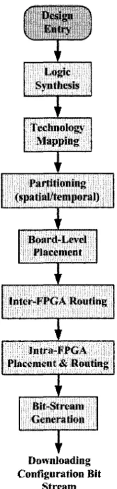
2.3 CAD Flow for Logic Em ulation S y s te m s ... 26
2.3.1 Introduction ... 26
2.3.2 CAD Flow for F B E s ... 27
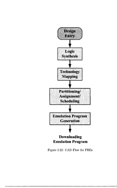
2.3.3 CAD Flow for P B E s ... 32
3 A r ch itectu r e o f H y b rid E m u la tio n P r o c e sso r (H E P ) 35 3.1 Top-Level Organization th e Em ulation E n g in e ... 35
3.2 How a Logic Design is E m u la te d ? ... 36
3.3 S tructure of H ybrid Em ulation Processor ... 37
3.4 Instruction Set A rchitecture of H E P ... 39
3.5 C entral Control U nit of H E P ... 42
3.6 Control Memory of H E P ... 48
3.7 D a ta Memory of H E P ... 49
3.8 In p u t/O u tp u t P o rts of H E P ... 50
3.9 H E P ’s Program Counter Register (Global S equencer)... 51
3.10 Additional Signal Pins of H E P ... 52
4 I m p le m e n ta tio n o f H yb rid E m u la tio n P ro c esso r on F P G A 54 4.1 In tro d u c tio n ... 54
4.2 Design Specifications for H EP-based Em ulation E n g in e ... 55
4.3 RTL Design of H EP-B ased Em ulation E n g in e ... 57
C O N TEN TS
4.4 RTL Simulation R e s u l t s ... 59
4.5 Synthesis R e s u l t s ... 60
4.6 Com parison and C o n c lu sio n ... 66
5 A C A D T o ol S u ite for H E P -b a se d E m u la tio n S y s te m 69 5.1 Basic requirements for H EP-based CAD tool ... 69
5.2 Overall CAD F l o w ... 71
5.2.1 Design E n t r y ... 71
5.2.2 S y n th e s i s ... 72
5.2.3 Technology M a p p in g ... 73
5.2.4 Scheduling ... 75
5.2.4.1 P re lim in a rie s ... 77
5.2.4.2 Levelization ... 79
5.2.4.3 Modified List Scheduling ( M L S ) ... 84
5.2.4.4 M L S +B FF Scheduling ... 88
5.2.4.5 M athem atical F o r m u la tio n ... 89
5.2.4.6 Evaluation M e tric s ... 93
5.2.4.7 Im plem entation of M L S /M L S +B F F Scheduling T o o l s ... 95
5.2.5 Experim ental Results ... 95
5.2.6 Code G eneration and Download ... 100
5.3 Comparison and C o n c lu sio n ... 100
6 C o n clu sio n s an d F u tu re W ork 103 6.1 F uture Work ... 104
6.1.1 Im provements in H ardw are A rc h ite c tu re ... 104
6.1.2 Improvement in Design Compiler T o o l ... 104
R efere n c es 106
List of Figures
2.1 C om plexity/P roductivity growth versus tim e in term s of num ber of tran sisto rs[66] . 5
2.2 General view of software sim ulation tools ... 7
2.3 General view of a Logic Em ulation S y ste m ... 10
2.4 Logic em ulation system c o n n e c tiv ity ... 11
2.5 Internal view of a typical F PG A ... 12
2.6 S tructure of a 3-input LUT (k = 3 ) ... 13
2.7 Internal stru ctu re of a generic logic e l e m e n t ... 14
2.8 A generic FPG A -based logic em ulation system ... 14
2.9 Mesh a rc h ite c tu re ... 15
2.10 Internal stru ctu re of a field program m able interconnect device ( F P I D ) ... 16
2.11 Logical view of full crossbar interconnect (a). Block view (b )... 17
2.12 Logical view of partial crossbar interconnect (a). Block view (b )... 17
2.13 Exam ple of two-level hierarchical partial crossbar architecture... 18
2.14 Hybrid complete graph partial crossbar a r c h i t e c t u r e ... 19
2.15 A genric view of non-tim e-m ultiplexed signals among two p artitio n s... 20
2.16 Generic view of V irtual W ire a r c h i te c tu r e ... 21
2.17 Time-multiplexed F P G A configuration m odel... 22
2.18 General view of one logic element in a tim e-m ultiplexed F P G A ... 23
2.19 General view of a Homogeneous P B E s y s t e m ... 25
2.20 General view of a Heterogeneous P B E s y s t e m ... 26
2.21 CAD flow for F B E s... 31
2.22 CAD Flow for P B E s ... 34
LIST OF FIGURES
3.2 Internal stru ctu re of H EP Processor... 37
3.3 Exam ple of im plementing function F in a 4-input LU T... 38
3.4 Fields of LU TO P i n s t r u c t i o n ... 40
3.5 Fields of RA M REF i n s t r u c t i o n ... 40
3.6 Fields of R O M R EF i n s t r u c t i o n ... 41
3.7 Fields of N O P i n s t r u c t io n ... 42
3.8 H E P ’s Control U nit Finite S tate M a c h i n e ... 44
3.9 H E P ’s Control Memory stru c tu re ... 49
3.10 H E P ’s D ata M emory stru ctu re... 50
3.11 H E P ’s In p u t/O u tp u t stru ctu re... 51
3.12 H E P ’s P rogram Counter (Global Sequencer)... 52
3.13 H E P ’s Pin-out M ap... 53
4.1 Generic architecture of H EP-based em ulation e n g i n e ... 55
4.2 Exam ple of Signal Trap c ir c u itr y ... 56
4.3 F P G A Design F lo w ... 58
4.4 Hierarchy of VHDL design files for H EP P r o c e s s o r ... 59
4.5 Exam ple of 4x4 Sequential B inary M ultiplier ... 60
4.6 Simulated waveform view of P rogram C ounter S u b m o d u le ... 61
4.7 Simulated waveform view of 4-input L U T ... 61
4.8 Simulated waveform view of 64-input interconnect switch ... 61
4.9 Simulated R ead/W rite cycles of ID R and L D R ... 61
4.10 Simulated R ead/W rite cycles of Left Control M e m o r y ... 62
4.11 Simulated R ead/W rite cycles of Right C ontrol Memory ... 62
4.12 Simulated functionality of C entral Control U nit while executing a L U T O P instruction. 63 4.13 Simulation of em ulation program being D ow nloaded/Executed on a processor . . . . 63
5.1 Design cycle versus Em ulation Cycle in a generic D U T ... 70
5.2 CAD Flow for H EP-based em ulation system ... 71
5.3 RTL view of binary m ultiplier produced by Synopsys Design C o m p ile r ... 72
5.4 Gate-level view of binary m ultiplier generated by Synopsys Design C om piler... 73
5.5 Exam ple of technology m apping for reducing area and delay. ... 75
5.6 Technology decomposition, (a) Balanced-tree, (b) U nbalanced-tree... 76
LIST OF FIGURES
5.8 DAG representation of n e t l i s t ... 79
5.9 Instruction memory map (IMM) of H EP-based em ulation system ... 80
5.10 ASAP L e v e liz a tio n ... 81
5.11 ASAP algorithm in pseudo code... 82
5.12 ALAP L ev e liz a tio n ... 82
5.13 ALAP algorithm in pseudo code... 83
5.14 Processor workload after levelizing “elliptic” ... 83
5.15 MLS a l g o r i th m ... 85
5.16 Examples of collapsing nodes during IMM allocation... 87
5.17 Prioritizing nodes with equal m obility w ith respect to their fan-out degree... 90
5.18 M LS+B FF algorithm ... 91
5.19 Executing program on a parallel p l a t f o r m ... 94
5.20 Example of o utp u t generated by GSchedule to o l... 96
List of Tables
4.1 Synthesis results of H EP processor and subm odules... 64
4.2 Synthesis results of H EP-based em ulation system ... 65
4.3 Comparison of H EP w ith other E m ulation s y s t e m s ... 68
5.1 Ten biggest MCNC circuits... 74
5.2 Results of technology m apping... 76
5.3 Processor workload calculated after MLS scheduling... 97
5.4 Processor workload after MLS scheduling on m ultiplier... 97
5.5 Processor workload after M L S + B FF scheduling... 98
5.6 Em ulation tim e and speed-up obtained by MLS scheduling... 99
5.7 Em ulation tim e and speed-up obtained by M LS+B FF scheduling... 99
L is t o f A b b re v ia tio n s
A bbreviation Definition
C L Critical p ath length.
P Num ber of H EP processors.
W Number of instruction words per HEP.
t Processor workload.
4> Average processor workload.
A Speed-up.
ALAP As-Late-As-Possible (levelization). ASAP As-Soon-As-Possible (levelization). ASIC Application-specific integrated circuit. BDD B inary decision diagram.
B F T B readth-first traversal.
BLIF Berkeley logic interchange form at. CAD C om puter aided design.
CMC C anadian microelectronics corporation. CPN Critical p ath node.
LIST OF ABBREVIATIO NS
A b b reviation D efin ition
EDA Electronic design autom ation. F B E FPG A -based em ulation system. F F Flip-flop.
F PG A Field-program m able gate array.
F PID Field-program m able interconnection device. FSM F inite state machine.
H C G P Hybrid Complete G raph P artial Crossbar. H EP Hybrid Em ulation Processor.
HOL Higher-order logic. IC Integrated circuit. ID R Input d a ta RAM. I/O In p u t/o u tp u t.
IE E E In stitu te of electrical and electronics engineers. IMM Instruction memory map.
LDR Local d a ta RAM. LE Logic element. LSB Least significant bit.
LSI Large scale integrated (circuit). LUT Look-up-table.
MCNC Microelectronics center of N orth Carolina. MFS M ulti-FPG A system.
MIMD M ultiple instruction m ultiple data. MLS Modified list scheduling.
MSB Most significant bit. MUX Multiplexer.
P B E Processor-based em ulation system. P E Processing element.
RTL Register transfer level. T P G Task precedence graph. TTL Transistor-Transistor Logic.
C h a p ter 1
I n tr o d u c tio n a n d M o tiv a tio n
Ever since digital VLSI circuits came into existence engineers have been facing the constantly growing
problem of verifying correct functionality of circuits before they are sent for fabrication. Once the
chip is fabricated, which is a very expensive procedure, it would be impossible for designers to modify
th e hardw are in case design errors were detected, unless th ey go through all the design steps again. Several functional verification methodologies such as software sim ulation and hardw are-accelerated
sim ulation have been proposed so far. Each m ethod has a num ber of advantages as well as disadvan
tages. A briefly review of all these m ethods is presented in future chapters. Traditional verification
m ethods are not effective for very large IC designs. Consequently, finding faster, cost effective and
more accurate solutions for design verification is a very im portant research issue.
T he m ost effective m ethod for performing functional verification of an IC design prior to fab
rication is Logic Emulation. A logic em ulation system (also known as logic em ulator) is a field program m able system th a t can be program m ed to em ulate (i. e. im itate) the functionality of a
digital circuit a t speeds of millions of cycles per second(CPS).
During p ast few years m any logic em ulation systems have been proposed and implemented. The
two m ain classes of logic em ulation systems are FPGA-based logic emulation (FBE) and processor-based logic emulation (PB E) systems. Each of these system s have a number advantages as well as disadvantages. In m ost cases these systems might be so complex and expensive th a t it would be
financially infeasible for small or medium size companies to afford. Currently, there is a dem and
1. IN TRO D U C TIO N A N D M OTIVATION
multi-million gates.
More im portantly, all logic em ulation systems have an associated set of m apping CAD tools
(called design compilers) th a t perform the task of design compilation. T he design compiler reads the
netlist of th e design under fesf(DUT) and autom atically converts it to a downloadable bit-stream th a t can be “program m ed” into th e logic em ulation system. Once th e logic em ulation system is
program m ed, design engineers can verify th e functionality of D U T by “running” it on the em ulation
system. Much work remains to be done in exploring new architectures and m apping CAD tools for
logic em ulation systems.
1.1
T hesis O verview
The m ain goals of this thesis are:
1. Investigate a cost effective architecture for processor-based logic em ulation system s targeting
FPG A s. The m otivation is to combine the advantages of both FB Es and P B E s in a single system.
2. C reate a CAD framework for autom atic m apping of D U T netlist to a targ e t processor-based
logic em ulation system.
3. Explore new scheduling algorithm s for m apping design netlists into a collection of parallel
processors.
In th e first p a rt of this research, a hardw are architecture for processor-based logic em ulation system
has been proposed which was implemented in Xilinx V irtex-II and V irtex 4 FPG A s. Efficiency of
proposed architecture in term s of speed, area and other design constraints is compared w ith other
studies.
More im portantly, based on the proposed architecture, a software CAD framework th a t can auto m atically m ap a gate-level netlist into a series of instructions, which can be executed in parallel on a
1. IN TRO D U CTIO N A N D M O TIVATION
1.2
T hesis O rganization
This thesis is organized as follows:
In C hapter 2 the history and im portance of functional verification is briefly reviewed and various
hardw are architectures for logic em ulation systems are presented. T hen th e CAD flow and algorithm s
used in each class of logic em ulation system is discussed. In C hapter 3, th e hardw are architecture
proposed in this research is explained and later in C hapter 4 th e im plem entation results of the
proposed architecture are described. C hapter 5 covers the CAD framework for m apping design netlists on to the targ e t logic em ulation system. Also, two scheduling algorithm s are introduced and
explained in detail as to how they improve the em ulation speed. T he experim ental results obtained
C h a p ter 2
B a ck g ro u n d a n d P r e v io u s W o rk
In 1965, Gordon Moore predicted th a t th e num ber of transistors per unit area in a typical inte
grated circuit (e. g. microprocessor) will double roughly every 18 m onths [51]. This increase in the integration level is called semiconductor productivity [35], or b etter known as M oore’s law. A nother im plication of semiconductor productivity is th a t greater functionality is being integrated into unit
area of semiconductors, which results in a direct increase in design complexity. Therefore, some
researchers refer to such trend in semiconductor productivity as complexity growth.
On the other hand, the term design productivity refers to th e num ber of logic gates designed
by single designer per day [35], Statistics from real world show th a t although sem iconductor pro
ductivity keeps increasing w ith th e pace expected by the M oore’s law, design productivity is not
improving proportionally, resulting in w hat we would like to call production gap or, as it will be
explained shortly, verification gap (Fig. 2.1). T he existence of such a gap is due to two m ain rea sons: first, increase in th e number of circuit elements and their interconnection (i. e. design size).
Second, increase in th e num ber of te st vectors to verify th e correctness of all circuit elements. For
example, if there are N circuit elements (such as logic gates or flip-flops) w ithin the digital circuit
under te st and each element can assume a binary value (0 or 1), th en we need a t m ost 2N test vectors to thoroughly verify the functionality of the circuit. It goes w ithout saying th a t even for a very small circuit ( N < 100) it is practically impossible to fully verify th e correctness of the design as the number of test vectors (2100) is alm ost infinite. To avoid design errors and possible
2. BAC KG RO U N D AN D PREVIO US W O R K u im « a & im o
. "tm*
•m
e
93 E"“* v 'Sco t«Sim o M
1000M
100M
10M
-l M - 0.1M - 0.01 Ml
58% / Yr. Complexity Growth Rate
21% / Yr. Productivity Growth Rate if* a© «r>. s T v.
- IOOOO0K
- 1OO0OK -1000K - 1O0K
- 0.1 K
CUIIK
jjj
5 y tm» “t
6 © ST a
*T! ©
?5i © Sf 5
S. -•
2
g*
©
a
Figure 2.1: C om plexity/P roductivity growth versus tim e in term s of num ber of tran sisto rs[66]
designs before fabrication, often referred to as design verification. In fact, it would be fair to say
th a t, design verification has become the m ost im portant bottleneck in the design process, requiring
about 60-75% of design resources such as design time, com puting resources and man-power [53] [41].
Therefore, m any researchers are targeting this area to narrow the verification gap or at least keep it from increasing as th e design size grows.
2.1
H istory o f D esign Verification
There are m any different ways for tackling th e design verification problem , some of which have been
around for a while. In general, there are five different m ethods used for design verification:
1. Formal Verification
2. Simulation
3. Hardw are Accelerated Simulation
4. Rapid Prototyping
5. Logic Em ulation
Each m ethod has a num ber of advantages as well as drawbacks. In th e sem iconductor and electronic industries, some or all of these m ethods are used to verify designs, based on design complexity and
2. BA C K G R O U N D AN D PRE VIO U S W O R K
2.1.1
Formal V erification
Formal verification refers to a process through which a designer proves formally th a t a designed
circuit satisfies the design specifications for all possible inputs [41]. T he behavior of a hardw are
design is described formally and then the correctness of the design is proved by using a number of m athem atical proof techniques [71] [27]. In formal verification, first th e hardw are is represented
using, logic equations or fin ite state machines (FSMs), regardless of other design aspects such as
tim ing or area constraints. Then, th e designer studies th e question of w hether the designed circuit
matches th e specifications or not. T he specifications are often w ritten as a set of tem poral logic formulas. For obvious reasons, some researchers believe th a t formal verification m ethods are simply
p arts of th e design process and not a post-design process.
Two most common approaches for formal verification are theorem proving (algorithm ic veri
fication) and model checking (deductive verification). Model checking tools represent th e design
using Binary Decision Diagrams (BDDs) and the specifications by a set of tem poral logic formulas
[10] [15]. The model checking tool th en traverses th e BDD by exploring all possible combinations of in p u ts/sta te s/o u tp u ts to verify if the formulas are satisfied. O n the contrary, in theorem proving
techniques, both the hardw are and its specifications are represented in some ab stra ct logic such as
Higher-Order Logic (HOL). Then, a m athem atical proof w ithin the rules of th a t logic is constructed th a t shows the design m atches its specifications. Theorem proving tools autom ate the process of
establishing the proof [23].
Since formal verification m ethods use m athem atical approach to determ ine the correctness of a
design, therefore all possible errors in th e design will be detected and sound functionality of the
design is guaranteed. However, they have a num ber of drawbacks which limit th eir usage for real world designs. For instance, formal verification m ethods are not easily scalable and they all suffer
form state-space explosion. T h a t is, if there are 250 memory cells w ithin the circuit, then the
circuit would have 2250 states 1 th a t need to be exhaustively searched. On th e other hand, finding
m athem atical abstraction (model) for even a small design is a complicated and tedious task and
requires lots of knowledge and experience. To overcome these problems, researchers have tried to
combine different formal verification m ethods together [23], bu t th e results are still not suitable for
large designs.
2. BAC KG RO U N D A N D PREVIO US W O R K
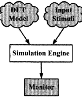
IlipUt
Stimuli
Monitor
Simulation Engine
Figure 2.2: General view of software sim ulation tools
2.1.2
Sim ulation
By far the most popular verification m ethod is software simulation, or simply, simulation. The inputs to a logic sim ulator are the design netlist file and input stimulus signals, often in the form of
vector d a ta files. The sim ulator com putes how the design-under-test (DUT) would operate over time and generates required outputs, given those inputs [4] [1]. It is then th e designer’s job to observe the
outputs produced by the sim ulator and verify if the design is operating correctly. The comparison
process can be autom ated by defining “m onitors” for the sim ulation tools. It should be emphasized
th a t, in the sim ulation technique, not only th e input stimuli to th e DUT are represented in software
(e. g. vector d a ta files) bu t also the D U T itself is represented in software. Therefore, it is obvious th a t th e simulator is nothing but a software sim ulation “engine” th a t runs th e models of a DUT
against given input vector files (Fig. 2.2). In more recent design methodology, designers use hardw are
description languages (HDL), such as Verilog or VHDL, to not only describe th e design, behaviorally or structurally, but also specify input stimuli and m onitoring routines w ithin th e same embodim ent,
called test bench (shown by shaded blocks in Fig. 2.2) [56]. Software sim ulators have a num ber of advantages over other verification tools:
• They provide extensive capabilities for modifying and debugging the design which is due to
the intrinsic flexibility in software.
• They are much easier to use.
2. B A C K G R O U N D AN D PREVIO US W O R K
The above benefits make sim ulators the m ost widely used verification tools. However, they do have
limitations:
• As the size of logic designs doubles th e am ount of com puting work to sim ulate them roughly
quadruples. A rough estim ation for such increase is th a t, an increase in th e num ber of logic gates not only increases the num ber of cycles, bu t also it increases the com putational work
per cycle to get acceptable coverage [48]. Hence, software sim ulators are sim ply too slow to
sim ulate designs w ith more th a n a million gates. Typically th eir sim ulation speed is around
tens of cycles-per-second(CPS).
• Sim ulators do not provide th e in-circuit em ulation(lCE) capability.
• The accuracy of simulation results depends solely on how well the designer has modeled the
DUT in software and the num ber of test vectors (input stimuli) provided. Therefore, user
expertise is a key factor in sim ulation accuracy.
If we only use sim ulators for design verification, it is very likely th a t some design errors rem ain undetected. A notorious example of such an incident was th e design bug in th e floating point
arithm etic unit of Intel’s Pentium processor, reported in [54], which caused a financial loss of several million dollars to the company.
2.1.3
H ardw are-A ccelerated Sim ulation
To overcome the speed lim itation of software simulators, sim ulation accelerators based on custom
hardw are were developed. These accelerators provided built-in te st equipm ent (such as signal gen
erators and logic analyzers). Instead of using com puter w orkstations, designers could execute th e
sim ulation of their designs on a num ber of parallel processors which run orders of m agnitudes faster
th a n sim ulators [3] [16] [61].
Although, hardware-accelerated sim ulators provided good speedup for sim ulation, they still suf
fered from two m ajor problems:
• It should be emphasized th a t hardw are-accelerated sim ulators are still using software models
of the design and not real hardware.
• Massively parallel processing platform s succeed in physical sim ulation such as fluid flow or structural analysis bu t they are not efficient enough in sim ulation of logic designs because logic designs have very irregular topologies [48].
2. BACK G R O U N D AND PREV IO U S W O R K
2.1.4
R apid P ro to ty p in g
A nother relatively less popular functional verification m ethod is rapid prototyping. In this m ethod
designers quickly produce hardw are models of th e actual product th a t is fabricated by using fast
prototyping platform s such as program m able logic technology. By examining th e functionality of
those models, designer can identify possible errors in their design before th ey send it for fabrication.
Unfortunately, the feasibility of rapid prototyping technique depends highly on th e type of the
application and availability of tools. In one example, researchers have created a flexible environm ent
to develop only digital signal processing (DSP) applications [33].
Since rapid prototyping requires building a hardw are sample closest to th e final product, th e
verification process will be fastest and detection of m ost design errors is likely. However, th e main
disadvantage is th a t once th e prototype is built it can not be used for other applications and therefore
it would be a throw-away effort.
2.1.5
Logic E m ulation
The m ost recent verification tools are logic emulation systems. A hardw are em ulator is a completely program m able hardw are system which can be program m ed to im itate (i. e. em ulate) the functionality
of a large digital design (tens of million gates) a t th e speed of m ulti million cycles per second (CPS).
In other words, a logic em ulator is a program m able device th a t, once program med, functions ju st like a prototype of th e final chip before actually fabricating the chip itself.
Logic emulation system s have a num ber of advantages over other verification tools th a t have recently brought them into spotlight. In the upcom ing sections we will be thoroughly investigating
the hardw are architecture and CAD tools for logic em ulation systems.
2.2
A rchitecture o f Logic E m ulation S ystem s
So far a number of hardw are architectures for logic em ulation systems have been proposed, and
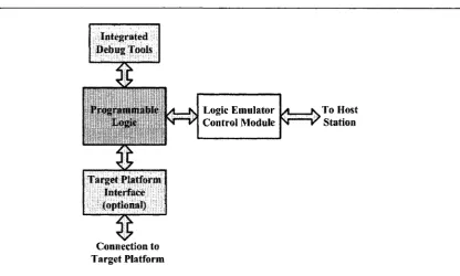
some of these architectures have been implemented. Regardless of th eir architecture, they all share a number of basic features. Generally speaking, a typical logic em ulation system consists of five
m ajor components which their connectivity is shown in Fig. 2.3.
1. Program m able hardw are
2. BACK G R O U N D AND PREVIO US W O R K
Integrated D ebug Tools
To Host Station
a k. Logic Em ulator
N— V C ontrol M odule
Target Platform Interface (optional)
Connection to Target Platform
Figure 2.3: General view of a Logic Em ulation System
3. Integrated instrum entation and debugging hardw are such as integrated logic analyzers (ILA) or program m able signal generators
4. Integrated control hardw are and software to support the run tim e environm ent of the em ulated
design
5. Target hardw are interface circuitry
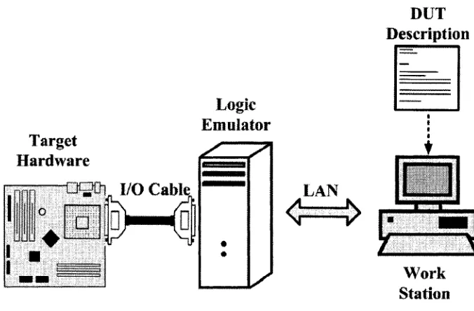
Figure 2.4 illustrates physical connectivity of a typical logic em ulator in th e real world environ
m ent. A logic em ulator can be either connected directly to a single w orkstation or a collection of w orkstations through a network (e. g. LAN), A set of back-end and front-end CAD tools run on
workstations. On th e other end, a logic em ulator can be connected to th e targ e t hardware, right in
the socket where the to-be-em ulated chip will be m ounted in future.
Logic em ulation systems are classified according to th e architecture used in their program m able
hardware. Although various companies and academic researchers have used different architectures,
they can all fall into one of th e following two categories:
1. FPG A -B ased E m ulators (FBE)
2. Processor-Based E m ulators (PBE)
As it will be explained later the proposed architecture combines some of the properties of both
2. BACK G R O U N D AN D PREVIO US W O R K
DUT
Description
Target
Hardware
Logic
Emulator
O'jO-1 I/O Cable
LAN
<=>
□
Work
Station
Figure 2.4: Logic em ulation system connectivity
h y b r id logic e m u la tio n system.
2.2.1
F P G A -B a se d Logic E m u lation S y stem (F B E )
Ever since Field-Programmable Gate Arrays (FPG A s) were introduced in late 80s, they have been
extensively used in rapid prototyping and logic em ulation platforms. Since FPG A s are fundam ental
building blocks of FPGA-based em ulation system s(FBEs), first, we will briefly review the internal
structure of a typical F PG A chip.
2 .2 .1 .1 I n tr o d u c tio n to F ie ld -P r o g r a m m a b le G a te A rray
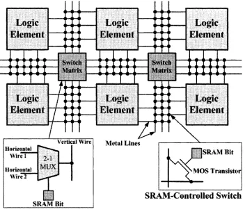
An F PG A is a flexible, completely re-program m able logic chip. W hile different F P G A m anufacturers
have introduced different architectures [55] [8], the most popular F PG A architecture contains a two
dimensional array of SRAM-based program m able logic elements (LE) (Fig. 2.5). The logic elements
are interconnected through horizontal/vertical m etal wires and SRAM-controlled interconnecting switches (shown at the bottom of Fig. 2.5).
Each logic element consists of two parts: a fc-input look-up table{LUT) and a flip-flop. A fc-input LUT consists of an array of 2fc x 1 SRAM-based memory cells. All k inputs to an LUT are address inputs to th a t memory array and the value read from a memory cell is th e o u tp u t of the LUT. A
2. BACK G R O U N D A N D PREV IO U S W O R K
Logic
Element
Logic
Element
Logic
Element
Logic
Element
Logic
Element
M etai Lines
H o rizontal
W ire I SR A M B it
MUX
M O S T ransistor
SRAM-Controlled Switch
SR A M B it
2. BACK G R O U N D AN D PRE VIO U S W O R K
8x1 Memory Bit
A
- B-
C-1 1 0
1 0 0 1 1
F=A*B+A-C+A-B
MGA
3-Input
Figure 2.6: S tructure of a 3-input LU T (fc = 3)
logic function directly into the m em ory array. An example of a 3-input LUT is shown in Fig. 2.6 th a t implements Boolean function F .
A combination of a fc-input LUT and a flip-flop is capable of producing all feasible com binational or sequential logic functions th a t can be built using fc input signals. The option of choosing between
th e combinational or sequential o u tp u t can be m ade by configuring the program m able bit connected
to th e o u tp u t multiplexer shown in Fig. 2.7. Typical LUTs have three to six inputs (3 < fc < 6), however it has been shown the best perform ance-versus-area is achieved by having fc = 4 [60].
Along w ith the program m able logic described above, an F P G A includes a great num ber of SRAM- based program m able switches and interconnecting switch m atrices (shown a t the bottom of Fig. 2.5)
which enables arb itrary interconnection among logic elements. T he process of interconnecting logic
elements together is called routing. A t th e perim eter of an F P G A chip, program m able I /O pins connect th e F P G A ’s internal logic to th e outside circuitry. Based on th e above descriptions, it is
obvious th a t an F PG A is a highly program m able device th a t can be configured (program m ed) to
implement any digital circuit.
It should be emphasized th a t commercially available FPG A s are much m ore com plicated in architecture. They usually include em bedded memory blocks, dedicated fast logic for arithm etic
operations as well as complicated logic element architecture. Medium-size commercial FPG A s have a logic capacity of few thousands logic elements equivalent to few tens of thousands logic gates[20] [39]. A lthough this capacity might sound large enough for some applications, it is not big enough for most
2. BACK G RO U N D A N D PREVIO U S W O R K
C onfiguration Bit
4~lnput
2-1
MUX
C o c k
O u tp ut
F lip-Flop
Figure 2.7: Internal stru ctu re of a generic logic element
Hardwire
Connection
Programmable
Interconnection
FPGA
FPGA
FPGA
FPGA
FPGA
FPGA
FPGA
FPGA
Figure 2.8: A generic FPG A -based logic em ulation system
higher logic capacities.
2 .2 .1 .2 A r c h ite c tu r e o f F P G A -B a s e d L ogic E m u la tio n S y ste m s
T he program m able hardw are section of FPG A -based em ulators consists of a collection of F P G A mod
ules interconnected through hardwires a n d /o r Field Programmable Interconnection Devices (FPID s)
(Fig. 2.8) [67][11][65],
From the architecture point of view, program m able interconnection devices are quite similar to program m able routing resources inside F P G A chips. In other words, an F PID is a collection of
program m able switches and switch m atrices. Thus th e com bination of m ultiple FPG A s and F PID s
2. BACK G R O U N D AN D PREVIO US W O R K
F PGA
F P G A
FPGA
F PGA
F PGA
F P G A
F P G A
, —
,r---F P G A
FPGA
TTT
Figure 2.9: Mesh architecture
The “routing architecture” of an FB E is the way in which the FPG A s, fixed wires and F PID s
are connected. Previous research has shown th a t the routing architecture has a strong effect on the speed, cost and routability of em ulation systems. This is because an inefficient routing architecture
may require excessive logic and routing resources when implementing circuits and cause long routing
delays. Increased routing delays will profoundly slow down th e em ulation speed.
Several routing architectures for FB Es have been proposed. T he routing architecture in FB Es
plays a key role in determ ining the cost and performance of these systems[70].
A M e s h I n te r c o n n e c t Early FB Es did not use any FPID s. Instead th e FPG A s were arranged in a two dimensional array and each F PG A was connected to its nearest neighboring FPG A s (mesh)
using hardw ired connections (Fig. 2.9) [34].
Although mesh architecture is simple, it has a num ber of lim itations which has m ade it obsolete.
In this architecture, F P G A I/O pins are not only used for connecting F P G A internal logic to
outside world, but also for routing inter-F P G A signals. Therefore a large percentage of F P G A I /O
pins will be used up for inter-FPG A routing purposes. Moreover, some nets might pass through m any interm ediate FPG A s in the mesh, which results in very long interconnect delays for some
signals. Not only does this slow down the design em ulation but also creates unbalanced propagation
delays among signals th a t can induce incorrect or unwanted behavior in some time-sensitive signals, (e. g. set-up/hold tim e violations).
pro-2. B ACK G RO U N D A N D PREVIO US W O R K
8 s —
9 £9 ! 9 i 9 I9 I 9 t3 I I
(9 E9 CI fi Ii 19 I1 t
lil,
SRAM Bit;
MOS Transistor:
Crosspoint Switch'
-I/O Pins
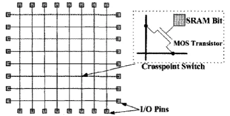
Figure 2.10: Internal stru ctu re of a field program m able interconnect device (FPID )
gramm ed (i. e. configured) to provide a rb itra ry connections between its I/O pins. It contains a
two dimensional array of, usually SRAM-based, program m able switches (Fig. 2.10). Therefore it is capable of making any one-to-one or one-to-m any connections between its I /O pins [21]. A typical F PID m ay have as m any as 1000 I /O pins.
In most recent F B E systems F PID s are being used for interconnecting signals among F P G A
pins. T he simplest architecture is Full Crossbar architecture. In this architecture each F P ID is
connected to “all” FPG A s on the em ulation board (Fig. 2.11). Since a full crossbar is capable of connecting any two pins in th e system it is logical to think of this architecture as a regular array
of program m able crosspoint switches. A lthough a full crossbar architecture guarantees successful routability of all nets, it is utilized in small em ulation systems w ith only a very few num ber of
FPG A s. This is because the size (area) of F P ID crossbar increases as the square of num ber of its
I/O pins. Equation 2.1 shows the relation between the num ber of crosspoint switches “5 ” in a full crossbar th a t interconnects “AT” FPG A s each w ith “P ” I /O pins.
S = N ( N - l ) P 2/2 (2.1)
For example, to interconnect 20 FPG A s (note th a t the num ber of F PG A s in a typical FB E
system is far more th an this), each with 200 I/O pins, we need a F PID m odule w ith 4000 I/O pins and a switch capacity of 7,600,000. M anufacturing such F PID would be im practical and expensive
in term s of pin count and layout area.
C P a r t i a l a n d H ie r a r c h ic a l P a r t i a l C r o s s b a r T he partial crossbar architecture [65] [42] over comes the lim itations of the full crossbar by using a set of smaller crossbars. This is due to the fact
2. BAC KG R O U N D A N D PRE VIO U S W O R K
F P G A
2
F P G A
3
F P G A
I
F P G A
4
F P G A F P G A
I -a'2 .;:g
)
-— —
F P ID
<
F P G A F P G A
3 4
* ~ Crosspoint Switch
(b)
Figure 2.11: Logical view of full crossbar interconnect (a). Block view (b).
FPG A 3
A B C F P G A 1
A B C
F P G A 2
A B C
A ll sw itch es b elonging to sam e group are
p laced in one FPID .
FPG A 1 F P G A 2 F P G A 3
PI
u
PIIJ
(b)
Figure 2.12: Logical view of partial crossbar interconnect (a). Block view (b).
is connected to a single FPID . Therefore th e num ber of F PID s in partial crossbar architecture is equal to th e number of subsets (Fig. 2.12).
P artial crossbar architecture maximizes the use of the F P G A ’s logic capacity. T he delay for any inter-F P G A connection is uniform and is equal to delay through one FPID . In this architecture,
th e size of FPID s increases only linearly as a fraction of the num ber of FPG A s. Also, since this
architecture is completely symmetrical, the m apping CAD tools can m ap a DUT into F B E in less
t im e . C o n s e q u e n t ly , t h e p a r t ia l c r o s s b a r in t e r c o n n e c t is e c o n o m ic a l a n d f u lly s c a l a b l e . H o w e v e r , it
has some disadvantages too. F irst is the ex tra cost and size of m ultiple FPID s. A nd second, the
fact th a t direct connections between FPG A s for routing time critical signals are not available.
2. BAC KG R O U N D A ND PREVIO U S W O R K
Layer 1
F P ID A F PIDHM D n
Off-Board Connection
Figure 2.13: Exam ple of two-level hierarchical partial crossbar architecture.
of partial crossbar. Instead, the partial crossbar architecture can be applied recursively, in a hier
archical m anner. T h a t is, each set of FPG A s and FPID s, interconnected through partial crossbar
architecture, could be virtually considered as a very large FPG A . A group of such “u ltra-F P G A s”
can be interconnected by a second level of FPID s, as shown in Fig. 2.13.
In th e example shown in Fig. 2.13, if there is a net th a t m ust be routed from ’’F P G A 2” to
’’F PG A 7” , then th a t signal should pass through two F P ID s a t ’’Layer 1” and one F P ID a t ’’Layer
2” , imposing a to tal of 3 unit delays on th a t signal. This implies th a t the more hierarchy levels are
used for interconnection, more delays would be induced on th e nets. B ut this delay is acceptable because th e size of flat partial crossbar cannot be scaled beyond a few tens of FPG A s.
D H y b r id C o m p le te G r a p h P a r t i a l C r o s s b a r T he latest research shows th a t a m ixture of
hardw ired and program m able connections among FPG A s provides a superior routing architecture for
FB E systems. In this approach, a significant percentage of pins in each F P G A are connected using hardwired, th e remainder are connected using program m able connections. T he hardw ire connections
are usually used to route tim e critical nets, whereas other non-critical nets are routed through F P ID s
(Fig. 2.14).
In hybrid complete graph partial cras.s6ar(HCGP) architecture, the key param eter, which affects
t h e d e g r e e o f r o u t a b ilit y , is t h e p e r c e n t a g e o f p r o g r a m m a b le c o n n e c t io n s P p w i t h r e s p e c t t o t h e t o t a l
num ber of interconnection (eq. 2.2-2.4). Results show th a t th e ratio of 60 percent provides good
routability and speed [42].
2. BACK G R O U N D A N D PREVIO U S W O R K
Hardwire Interconnections
Program m able Interconnections
'PH
PI I
FPGA 1 FPGA 2 FPGA 3
Figure 2.14: Hybrid complete graph partial crossbar architecture
Pp = N p/ N t (2.3)
Pp « 0.6 (2.4)
Where,
N p :Number of program m able connections
Nh :Number of hardw ired connections
N t :Total Num ber of Connections
E V i r t u a l W ir e A r c h i te c tu r e T he logic capacity (determ ined by th e num ber of logic elements)
of even th e high end F P G A chips is not large enough to em ulate even medium size digital IC designs.
Hence, FPG A -based logic em ulators m ust contain multiple FPG A s (tens to hundreds) so th a t they could em ulate multi-million gate logic circuits. Obviously, for such circuits, the design netlist m ust
be broken down in to smaller sub-circuits so th a t each sub-circuit could fit into single FPG A . T he process of breaking down a circuit netlist into smaller sub-circuits is referred to as partitioning.
Similarly, each sub-circuit is called a partition. After th e circuit netlist is partitioned and m apped
into FPG A s, they will be connected to each other through F PG A I/O pins. For each I/O signal
belonging to a partition, one I/O pin will be utilized (Fig. 2.15). Since FPG A s have limited num ber
of I/O pins, th e sum of inputs and o u tp u ts of each partitio n can not exceed the num ber I/O pins in one F PG A . Therefore, while partitioning a circuit am ongst m ultiple FPG A s, each p artition should
satisfy two constraints:
1. Logic capacity constraint:
2. BAC KG RO U N D AND PRE VIO U S W O R K
FPGA #!
FPGA #2
I I
Physical W ires
Figure 2.15: A genric view of non-tim e-m ultiplexed signals am ong two partitions.
2. P in constraint: jVj + N 0 < Pt where,
N i -.Number of Inp u t signals to partition
N 0 :Number of O u tp u t signals from partitio n
Pt :Total num ber of F P G A I/O pins
In a paper by Landm an and Russo [46], it was empirically shown th a t the num ber of I /O pins
in a p artition is a function of num ber of logic elements in th a t partition. Such relation is shown in 2.5 and it is referred to as “R e n t’s rule”.
Pt = k x L R (2.5)
where,
L : Total num ber of logic elements
R :Rent’s constant (0.4 < R < 0.8)
k : average fan-in of logic elements
Em pirical results show th a t, due to R ent’s rule, a great percentage of F P G A logic capacities in
conventional FBEs will rem ain underutilized. In worst cases it could be as high as 80%.
To overcome pin lim itations (expressed by R ent’s rule) and improve logic utilization in FPG A s, researchers a t M IT proposed the idea of Virtual Wires [2]. Unlike trad itio n al architectures where each interconnecting physical wire is assigned to one signal (net), in virtual wire architecture each
physical wire will transfer multiple signal values a t different tim e slots. In other words m ultiple
2. B AC K G R O U N D AND PRE VIO U S W O R K
FPGA #1
FPGA #2
Logical Outputs
I
I
I
T
A
Logical Inputs
J f t t
---
-»►
Serial Shifter
Serial Shifter
Physical Wire
Figure 2.16: Generic view of V irtual W ire architecture
registers are th en serially transferred to the “destination” partition. A single wire is used to transfer
th e serial values from the “source” partitio n into th e “destination” partition. At the “destination”
p artition th e signal values are De-multiplexed using a set of serial receivers and a serial-to-parallel
converters. It should be m entioned th a t th e sampling and transm ission of signal values takes place during each design’s clock cycle.
V irtual wire-based architecture has a num ber of advantages over other architectures such as:
• It significantly improves logic utilization in FPG A s (some cases m ore th a n 45%).
• Overcomes I/O pin constraints.
• Significantly reduces th e num ber of FPG A s required in th e F B E systems. Therefore virtual wire-based em ulators are much smaller and cheaper.
O n th e other hand virtual wire-based em ulators have a num ber of disadvantages too:
• E x tra control circuitry inside each F P G A is needed to tim e m ultiplex/de-m ultiplex signals on
a shared wire which imposes logic overhead in the circuit.
• Transferring signal values in tim e slots will cause delay in th e signals. Therefore, em ulation
speed is reduced.
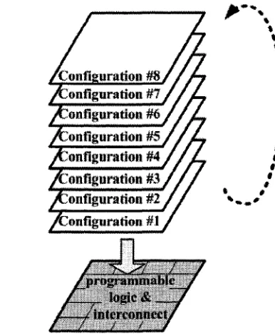
F T im e - M u ltip le x e d F P G A A r c h i te c tu r e In a different approach to improve logic u ti
liz a t i o n in F P G A s , r e s e a r c h e r s h a v e p r o p o s e d a d y n a m ic a l ly r e c o n f ig u r a b le F P G A c a lle d
time-multiplexed FPG A [64]. At any instance of time, a time-m ultiplexed F P G A has one “active” configuration
and eight “inactive” configurations. T he configuration mem ory (also referred to as configuration
2. BACK G R O U N D AN D PREVIO US W O R K
t
* %
i
i f
*
i
*
*
#
* *
Figure 2.17: Time-m ultiplexed F P G A configuration model.
chip which might contain 100,000 m em ory cells. Each configuration m em ory cell is backed up by
eight inactive configuration m emory cells. W henever th e F P G A is reconfigured, all th e logic elements
and interconnecting switches are updated sim ultaneously through th e contents of one configuration
memory plane (Fig. 2.17). In practice, inactive configuration bit-stream s m ight be stored in off-chip m em ory banks which increases the F P G A reconfiguration delay.
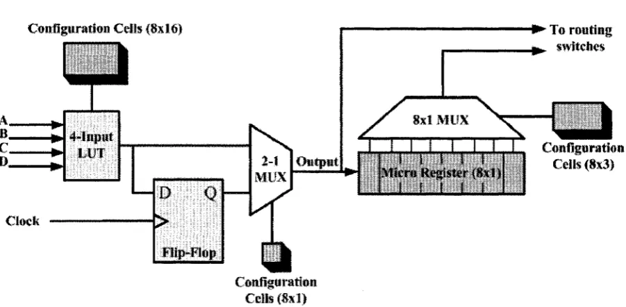
After each and every reconfiguration, the outp u t of each logic element inside the F PG A is also stored in memory arrays called micro-registers. W ith 8 configuration planes, a micro-register should
contain an array of 8 x 1 memory cells. A general stru ctu re of a logic element in a time-m ultiplexed
F P G A is shown in Fig. 2.18.
In logic em ulation mode, the tim e multiplexing capability of th e F P G A is used to em ulate a
large design. The F P G A sequences through all configurations called micro-cycles. P artial results after each micro-cycle (i. e. after one configuration of th e device) will be saved in micro-registers
and passed to subsequent micro-cycles. One pass though all micro-cycles is equivalent to one DUT
clock cycle (also known as user cycle).
2 .2 .1 .3 E m u la tin g L og ic D e sig n s o n F B E s
So far we have explained different architectures used in th e program m able hardw are section of FBEs. Now we explain how a typical digital design can be em ulated on a generic FB E. To em ulate a logic
rC onfigu ration
i # 7 ,
/ £ o n t i g u r a tion #5*
i # 4,
T ^ n f i i S r i o n #
i# l
prograinniabU
logic &
2. BACK G R O U N D A N D PREVIO U S W O R K
C onfiguration C ells <8x161 *► T o routing
^ sw itches
8x1 M U X
2-1
M UX
O u tp u t
C lock
4-in p u t
LUT
Flip-Flop
M icro K egister <8xl)
C onfiguration C eils (8x1)
Figure 2.18: General view of one logic element in a tim e-m ultiplexed FPG A .
design on an FBE, first, th e m apping CAD tools tran slate the design netlist into a set of configuration
bit-stream s th a t can be used to configure (i. e. program ) th e FPG A s and FPID s. Then, program m ing
bit stream s are downloaded into all FPG A s and FPID s. Once the FBE is configured it is ready to
em ulate th e design. T hrough a set of run-tim e tools, designers can examine their designs and detect possible errors. We will explain the details of th e steps involved in future sections.
2.2.2
P ro cesso r-B a sed Logic E m ulation S y stem (P B E )
The second class of logic em ulators are Processor-Based Em ulator System s (PBEs) [70]. F irst gen erations of PB Es were introduced to th e industry much before FB Es bu t they were only capable
of performing sim ulation acceleration and not in-circuit emulation. After the invention of FPG A s,
most companies preferred using FB Es for design verification. However, shortly later on, due to ob
vious disadvantages of FB Es as well as introduction of custom IC design, PB Es were brought back
into spotlight. As of mid 90’s (until now) m ajor verification vendors have introduced large-scale
high-end P B E systems to th e market[24].
A general misconception does exist among few engineers th a t needs to be addressed here. Some people believe th a t P B E system s are ju st another kind of hardware-accelerated sim ulation engines which is not correct. Here are some fundam ental differences between PB Es and hardw are-accelerated
simulators:
2. B A C K G R O U N D AND PRE VIO U S W O R K
which are optimized for em ulating the functionality of logic circuits, as opposed to hardw are-
accelerated machines in which generic processors are utilized.
• H ardware-accelerated sim ulators use software models of D U T com ponents to sim ulate th e
functionality of the whole design, whereas, in PB Es, the DUT netlist is directly m apped into hardware.
• Hardware-accelerated sim ulators can not be connected to targ e t platform and their o u tp u t
appears, usually, in form of signal waveforms or d a ta files, m onitored on w orkstation screens,
whereas, P B E s can actually be connected to th e targ e t hardware.
As it will be explained in forthcoming chapters, this research has introduced an easily im plem entable
architecture for certain class of PB Es which has in fact created th e required hardw are platform for
developing software CAD tools. B ut, before explaining th e proposed architecture, we will investigate th e generic architectures used in P B E s in this section.
2 .2 .2 .1 A r c h ite c tu r e o f P B E s
In P B E s a collection of highly parallel hardw are processors (e. g. tens to hundreds) are used to em ulate the functional behavior of logic designs. The processors com m unicate w ith each other during
run-tim e though an interconnection network. Depending on the logic processors ’ architecture, P B E
systems could be very simple in stru ctu re or very complicated. However, roughly speaking, P B E s
can be classified in two categories:
1. PB Es w ith Homogeneous A rchitecture
2. PB Es w ith Heterogeneous A rchitecture
A P B E s w ith H o m o g e n e o u s A r c h ite c tu r e In this architecture all logic processors (also
known as emulation processors) are identical in architecture (Fig. 2.19). Conventionally, each logic
processor is dedicated to em ulating the functionality of a single gate in the DUT. However, because
the processors are built using fast technologies, it is possible to use one processor to em ulate m ultiple gates a t different tim e slots. The control processor works as a bridge between th e host processor and
th e em ulation hardware. The I /O processor establishes in-circuit connection between the em ulation system and the targ et hardware. During the em ulation process, logic processors transfer signal values and other inform ation to each other.
Various em ulation systems used in industry are developed based on th e homogeneous architec