International Journal of Research in Advent Technology (E-ISSN: 2321-9637) Special Issue
National Conference “IAEISDISE 2014”, 12-13 September 2014
Quantum Dots: An Introduction
Manisha Yadav
1, Anita Chaudhary
2Department of Electronics & Communication Engineering1,2 Manav Bharti University, Solan (H.P.), India1,2
1
[email protected] 2 [email protected]
Abstract— The use of semiconductors has greatly increased in the last century. As new technologies start to rely more and more
on semi-conductors, their shortcomings are more and more apparent. Traditional semi-conductor devices have been found to be too big and too slow. As engineers search for a faster and more adaptable alternative to conventional semiconductors they have discovered quantum dots, a new form of semiconductors that model atoms. Being only nanometers in size, these pseudo-atoms take semi-conductors to a whole new level and can allow devices to work almost at the speed of light. Furthermore, quantum dots have numerous applications in optical technologies, mediums, and industries. This paper reviews the basics of quantum dot, its properties and some applications. Semiconductor quantum dot (QD) is a promising material for the next generation high speed optical communication devices.
Keywords— Quantum dot, Electronic state density, Quantum well, Quantum computing, Quantum dot Lasers, Quantum dot semiconductor optical amplifier.
1. INTRODUCTION
During the past few years, research in semiconductors has taken on, quite literally, new dimensions. Their numbers are two, one and zero. Electrons in recently developed devices can be confined to planes, lines or mathematical points- quantum dots [1].
Planes, lines and dots are mathematical constructs. They have no physical extent. How is it possible to make them in a real, three-dimensional material? The answer lies in quantum mechanics and Heisenberg’s uncertainty principle. The position of an object (an electron, for instance) and its momentum cannot both be known to arbitrary precision. As an electron is more closely confined, its momentum must be more uncertain. This wider range of momenta translates to a higher average energy. If an electron were confined in an infinitely thin layer, its energy would also be infinite.
In general, the energy of electrons in a semiconductor is limited by their temperature and by the properties of the material. When the electrons are confined in a thin enough layer, however, the requirements of the uncertainty principle in effect override other considerations. As long as the electrons do not have enough energy to break out of confinement, they become effectively two dimensional.
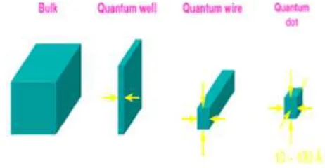
This locution is not just an approximation. Quantum well confines electrons or holes in one dimension and allow free propagation in two dimensions. Quantum wire confine electrons or holes in two spatial dimensions and allow free propagation in the third. Those confined in a quantum dot are not free in any dimension. This confinement is shown in Fig. 1. For common semiconductors, the length scale for a free conduction electron is about 100 angstroms. (One angstrom is meter, approximately the radius of a hydrogen atom.) An electron
inside a cube of semiconducting material 100 angstroms on a side is essentially confined to a point.
Quantum dots are man-made "droplets" of charge that can contain anything from a single electron to a collection of
several thousand [2]. Their typical dimensions range from nanometers to a few microns, and their size, shape and interactions can be precisely controlled through the use of advanced nanofabrication technology.
Fig. 1: Confinement of different structures.
2. HISTORY
Engineering of less than three-dimensional semiconductors began during the early 1970s, when groups at AT&T Bell Laboratories and IBM made the first two-dimensional “quantum wells”.
cadmium selenide. The samples had been subjected to high temperature; Ekimov suggested tentatively that the heating had caused nanocrystallites of the semiconductor to precipitate in the glass and that quantum confinement of electrons in these crystallites caused the unusual optical behaviour [1].
Ekimov’s hypothesis turned out to be true, but it took years of work by groups at Corning Glass, IBM, City College of New York and elsewhere to sort out the correct glass preparation techniques and convincingly demonstrate quantum confinement. Meanwhile Louis E. Brus and his co-workers at Bell Labs were making colloidal suspensions of nanocrystallites by precipitation from solutions containing the elements that make up semiconductors.
The term “quantum dot” was coined by Mark Reed.
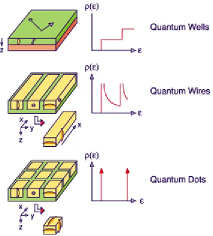
3. ELECTRONIC STATES DENSITY
The bulk semiconductors have the energy bands. MOCVD and MBE techniques provide an ability to control layer thickness to within 1 nm. When the thickness of the active layer is small enough then electrons and holes act as if they are confined to a quantum well. Such confinement leads to quantization of the energy bands into subbands. The main consequence is that the joint density of states ρ(ɛ) acquires a staircase-like structure [3]. Such a modification of the density of states affects the gain characteristics considerably and improves the laser performance.
Quantum well has continuous staircase-like electronic states density while the electronic state density of quantum dot is discrete. Fig. 2 shows the electronic state density of 2D, 1D and 0D confined structures [4].
Fig. 2: Electronic states density of 2D, 1D and 0D confined structures.
4. QUANTUM DOT: AN ARTIFICIAL ATOM
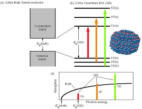
Quantum dots containing electrons can also be compared to atoms: both have a discrete energy spectrum as shown in Fig. 3 and bind a small number of electrons. In contrast to atoms, the confinement potential in quantum dots does not necessarily show spherical symmetry. In addition, the confined electrons do not move in free space, but in the semiconductor host crystal. Typical energy scales, for example, are of the order of ten electron volts in atoms, but only 1 millielectron volt in quantum dots. Quantum dots with a nearly spherical symmetry or flat quantum dots with nearly cylindrical symmetry can show shell filling according to the equivalent of Hund’s rules for atoms.
Fig. 3: Energy spectrum comparison
In contrast to atoms, the energy spectrum of a quantum dot can be engineered by controlling the geometrical size, shape, and the strength of the confinement potential. Also in contrast to atoms it is relatively easy to connect quantum dots by tunnel barriers to conducting leads, which allows the application of the techniques of tunnelling spectroscopy for their investigation. Like in atoms, the energy levels of small quantum dots can be probed by optical spectroscopy techniques. That’s why quantum dots are nicknamed as artificial atoms.
When photons are pumped into a semiconductor, electrons are excited into the conduction band, leaving behind holes in the valence band. Binding the electrons with their hole counterparts result in bounded electron-hole pairs, or excitons.
Quantum dots can best be described as false atoms. The primary material that a quantum dot is made out of is called a “hole”, or a substance that is missing an electron from its valence band giving it a positive charge. The primary material is extremely small, which is why it is called a dot, and at that size, electrons start to orbit it. Since quantum dots do not have protons or neutrons in the center, their mass is much smaller. Since the mass at the center is smaller than that of an atom, quantum dots exert a smaller force on the orbiting electrons causing an orbit larger than that of a regular atom (Fig. 4).
Fig. 4: The orbit comparison of quantum dot with hydrogen atom.
5. PROPERTIES
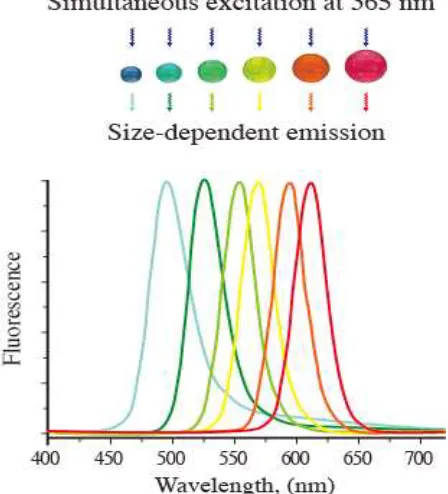
The composition and small size (a few hundred to a few thousand atoms) gives these dots extraordinary optical properties that can be readily customized by changing the size or composition of the dots. Quantum dots absorb light, then quickly re-emit the light but in a different color. Although other organic and inorganic materials exhibit this phenomenon— fluorescence—the ideal fluorophores would be bright and non-photo bleaching with narrow, symmetric emission spectra, and have multiple resolvable colors that can be excited simultaneously using a single excitation wavelength. Quantum dots closely fit this ideal. With a mass that small, scientists are able to precisely calculate and change the size of the band-gap of the quantum dot by adding or taking electrons. The band-gap of a quantum dot is what determines which frequencies it will respond to (Fig. 5 [5], [6]), so being able to change the band-gap is what gives scientists more control and more flexibility when dealing with its applications .
Fig. 5: Frequency and band-gap dependence.
One of the optical features of small excitonic quantum dots immediately noticeable to the unaided eye is coloration. While the material which makes up a quantum dot defines its intrinsic energy signature, more significant in terms of coloration is the size. Thus quantum dots of the same material, but with different sizes, can emit light of different colors. The physical reason is the quantum confinement effect. When electrons and holes (exciton pairs) generated by photons are confined within a space, or quantum box, smaller than the Bohr exciton radius (i.e., the normal, off-the-shelf, preferred, bulk material electron-to-hole distance of an exciton pair), the semiconductor's band gap widens and its fluorescence shifts towards the blue as shown in Fig. 6 & 7 [7]. The smaller that box, the bluer the fluorescence. Conversely, the looser the confinement, the bigger the quantum box, the redder the fluorescence. Eventually, one enters the infrared and the invisible. The fluorescence is generated when electron and hole recombine. The restricted confinement requires additional energy and this causes the wavelength shift.
advantageous for many applications. The future looks bright and exciting on all the possible applications of quantum dots.
REFERENCES
[1] Mark Reed, “Quantum Dots,” Scientific American, January 1993.
[2] Leo Kouwenhoven and Charles Marcus, “Quantum dots,” Physics world, June 1998.
[3] Govind P. Agrawal, “Fiber-Optic Communication Systems,” Willey Interscience; Third edition, 2002. [4] Yasuhiko Arakawa, “Connecting the dots,” Spie’s
oemagazine, January 2002.
[5] Richart E. Slusher, Ecole Normale Superieure, “Quantum Electronics,” IUPAP commission; April, 2005.
[6] Victor I. Klimov, “Nanocrystal Quantum Dots,” CRC Press, Second edition.
[7] Hideki Ooba, “Synthesis of Unique High Quality Fluorescence Quantum Dots for the Biochemical Measurements,” AIST TODAY Vol.6 , No.6 (2006) p.26-27.
[8] Nicole van der Laak, “A Quantum Dot: A Quantum what?”.
[9] Tomoyuki Akiyama, Mitsuru Sugawara and Yasuhiko Arakawa, “Quantum-Dot Semiconductor Optical Amplifiers,” Proceedings of the IEEE, Vol. 95, No. 9, September 2007.
[10] Brittany Webb, “Quantum Dots,” Departments of Chemistry and Physics, Utah State University.