DIWAN, MAITRIK Methodology for Analyzing Complex Algorithms for Small Satellites. (Under the direction of Professor Willam W. Edmonson).
From the view point of an electrical engineer, one of the main challenges in the field of space science is the mapping of complex control algorithms onto appropriate
hardware architectures. There is a wide knowledge gap between the team which de-signs these algorithms and the team which implements the algorithms. There is a
variety of hardware architectures available commercially onto which the algorithms
can be mapped. There also exist different design tools which can be used to perform
the implementation of these complex algorithms on appropriate hardware architec-tures. With the availability of a large suite of architectures and design tools, the
design engineer often gets puzzled in selecting the correct architecture and tools to
perform the implementation of the algorithm in an optimal manner.
This thesis presents a methodology for analyzing complex algorithms for small
satellite applications. The proposed methodology provides a step by step process of analyzing an algorithm for converting its Platform Independent Model (PIM) into a
Platform Specific Model (PSM). It assumes that the algorithm has been designed in
Simulink from Mathworks, which is the design tool of choice for aerospace system engineers engineers. After this, the methodology descibes the detailed process of
performing complexity analysis of the algorithm, which leads to identification of the
accelerator components. The next step explains the process of software and hardware implementation of the accelerator components. After this, the software and hardware
implementations are compared on the basis of Speed of Execution, Power Dissipation
and Development Time. The results are analyzed to make a decision regarding the implementation of the algorithm.
The proposed methodology is validated by applying it to the Atttitude
by
Maitrik Diwan
A thesis submitted to the Graduate Faculty of North Carolina State University
in partial fulfillment of the requirements for the Degree of
Master of Science
Electrical and Computer Engineering
Raleigh, North Carolina
2007
Approved By:
Dr. Winser E. Alexander Dr. William Rhett Davis
Dedication
To
Biography
Maitrik Diwan was born on December 25, 1983 in Ahmedabad, a city in the western part of India. He received his Bachelor of Engineering (B.E.) degree in
Elec-tronics and Communication from Nirma Institute of Technology (Gujarat University) in June 2005. He worked at the Physical Research Laboratory (A unit of Department
of Space, Government of India), Ahmedabad as a System Design Engineer for his
senior year project.
Maitrik joined NC State University, Raleigh in Fall 2005 to pursue graduate study
in Computer Engineering. Since Spring 2006, he has been working with Dr. William Edmonson in the field of design and development of small satellites. He has been a
part of a collaborative space based project between the North Carolina State
Uni-versity, the University of Florida, Gainseville, and the Defense Advanced Research
Acknowledgements
Above all, I thank my parents Jayshree Diwan and Yogesh Diwan for the much needed motivation throughout the duration of this project. It was their love and
support that helped me maintain sanity during stressful times. I would also like to
thank my dearest brother Prerak Diwan for his ever lasting support.
I sincerely acknowledge the efforts of Dr. William Edmonson, my academic
ad-visor, in providing guidance and encouragement for the successful completion of this thesis. Dr. Edmonson has made available all resources that I could possibly need
and also allowed the independence of applying my ideas in this project. I am deeply
indebted to him for his patience and invaluable suggestions during the course of this project. I am also grateful to the members of my thesis committee, Dr. Winser
Alexander and Dr. Rhett Davis for devoting their time and providing useful inputs.
I am highly greatful to all the members of HiperDSP Lab at NC State for providing
their support and encouragement during the course of my thesis. Special thanks to
Ramsey Hourani and Young Soo Kim, without whose support, my stay at HiperDSP lab would have been nearly impossible. They have always pointed me to the true
direction of research during the course of my thesis. Once again, I sincerely thank
Ramsey Hourani for all his academic as well as non-academic support. I would also like to thank Ravi Jenkal for his valuable sugesstions throughout the course of my
research.
I would also like to acknowledge the engineers at Xilinx Inc., M athworksr and Texas Instruments for providing technical support for the successful completion of my thesis.
Contents
List of Figures vii
List of Tables ix
1 Introduction 1
1.1 Motivation . . . 4
1.2 Related Work . . . 6
1.3 Contribution. . . 8
1.4 Thesis Organization. . . 9
2 Design Space Exploration 10 2.1 Choice of Hardware Architecture . . . 11
2.1.1 Time to Launch . . . 11
2.1.2 Performance . . . 11
2.1.3 Price . . . 12
2.1.4 Power Dissipation . . . 12
2.1.5 Feature Flexibility . . . 13
2.2 Architecture Exploration . . . 13
2.2.1 General Purpose Processors (GPP/RISC) . . . 14
2.2.2 Digital Signal Processors (DSP) . . . 14
2.2.3 Field Programmable Gate Arrays (FPGA) . . . 15
2.2.4 Application Specific Integrated Circuits (ASIC) . . . 16
2.3 Implementation Techniques . . . 17
2.3.1 Software Only Implementation . . . 19
2.3.2 Hardware Only Implementation . . . 21
2.3.3 Hardware-Software Co-Design . . . 22
4 FIR Filter Case Study 55
4.1 Code Comparison . . . 56
4.2 Software Code Optimization . . . 59
4.2.1 Development flow to increase performance . . . 60
4.2.2 Optimization techniques . . . 62
4.2.3 Summary . . . 68
5 Validation of Proposed Methodology 71 5.1 Overview of ADC Algorithm [1] . . . 71
5.2 Analysis of ADC algorithm. . . 75
5.2.1 Step 1: Choose candidate platforms . . . 75
5.2.2 Step 2: Algorithm analysis . . . 76
5.2.3 Step 3: Choose candidate accelerators. . . 78
5.2.4 Step 4: HW/SW implementation of accelerators . . . 81
5.2.5 Step 5: Comparative Metrics measurement . . . 100
5.2.6 Step 6: Analyze the results . . . 107
5.3 Conclusion . . . 115
6 Conclusions and Future Work 117 6.1 Conclusions . . . 117
6.2 Future Work . . . 120
List of Figures
1.1 Attitude Determination and Control system designed by AMAS . . . 5
2.1 Flexibility vs. Efficiency Tradeoff [2] . . . 18
2.2 Code Generation Process from Simulink Model [3] . . . 20
2.3 A generic high level synthesis system [4] . . . 22
2.4 Global Scheme for Codesign Methodology . . . 24
3.1 Overall flow diagram of the Proposed Methodology . . . 28
3.2 Concept Scoring Matrix . . . 30
3.3 Algorithm Analysis Flow . . . 32
3.4 Flow of data between DSP and FPGA . . . 37
3.5 Simulink model for Time Complexity Analysis . . . 38
3.6 Software Implemenation Process . . . 40
3.7 Hardware Implemenation Process . . . 42
3.8 FPGA Power Consumption Estimation using XPower . . . 50
3.9 Decision Making Flow . . . 52
4.1 Direct Form Implementation of a 6th order FIR filter . . . 57
4.2 Organization of hand written and tool generated codes . . . 59
4.3 Code Development Flow for TI C6xxx . . . 61
4.4 Code demonstrating Forward Store Optimization . . . 64
4.5 Code demonstrating Loop Unrolling . . . 65
4.6 Code demonstrating Index Updating . . . 67
4.7 Code demonstrating use of Intrinsics . . . 67
4.8 FIR filter design space . . . 70
4.9 Performance Improvement for FIR filter . . . 70
5.1 4 SGCMG cluster in a pyramid configuration. . . 72
5.2 High Level Block diagram of ADC algorithm . . . 73
5.3 Complexity analysis of Satellite Model . . . 77
5.5 Selection of Candidate Accelerators . . . 80
5.6 Optimizations performed on C matrix multiplication code. . . 84
5.7 Hardware Implementation of 3×3 matrix multiplication . . . 86
5.8 Software implementation of LU decomposition . . . 89
5.9 Hardware implementation of LU decomposition . . . 94
5.10 State Diagam of FSM I . . . 95
5.11 Hardware architecture of division module . . . 97
5.12 Max mul module . . . 98
5.13 Sub module . . . 99
5.14 Diagram to illustrate concept of power dissipation calculation . . . . 103
5.15 Execution Time analysis for Matrix Multiplication . . . 108
5.16 Power Dissipation analysis for Matrix Multiplication . . . 109
5.17 Execution Time − Power Dissipation curve . . . 109
5.18 Execution Time analysis for LU decomposition . . . 112
5.19 Power Dissipation analysis for LU decomposition . . . 113
List of Tables
1.1 Satellite Classification on the basis of weight . . . 2
2.1 Architectures and their Characteristics . . . 16
3.1 Characteristics and their numerical values . . . 29
3.2 Tabular representation for TI matrix system . . . 29
3.3 Different Categories of Time Complexities . . . 36
4.1 Differences between hand written and tool generated codes . . . 60
4.2 Clock cycles and Speedup for different Optimizations . . . 69
5.1 Time Complexity of blocks of Torque Generator . . . 79
5.2 Time Complexity of blocks of Steering Logic . . . 79
5.3 Design Space for Matrix Multiplication . . . 83
5.4 Hardware Implementation results for matrix multiplication . . . 87
5.5 Design Space for LU Decomposition . . . 92
5.6 Hardware Implementation results for LU decomposition . . . 100
5.7 Exection Times for Software Implemetations of Matrix Multiplication 101 5.8 Exection Times for Software Implemetations of LU decomposition . . 102
5.9 DSP power analysis for Matrix multiplication . . . 105
5.10 DSP power analysis for LU decomposition . . . 106
5.11 Code length comparison . . . 107
Chapter 1
Introduction
In the late 1980s, a new design approach for utilizing modern small satellites arose, and opened up a new class of space applications. One-of-a-kind, low-profile, low-cost
satellites, funded primarily by the Department of Defense (DoD) Advanced Research
Projects Agency, the Air Force Space Test Program, and university laboratories were built. The satellites were built to maximize the use of existing components,
off-the-shelf technology and minimization of non-recurring developmental effort. The
trend towards using small satellites continues today as evidenced by programs such
as the NASA Small Explorer (SMEX) Program and Earth Science System Pathfinder (ESSP), among others. NASA, DOD, foreign, and commercial developers of space
systems have all recently shown increased interest in small satellites as vehicles for
science, technology demonstration, remote sensing, and communications [5].
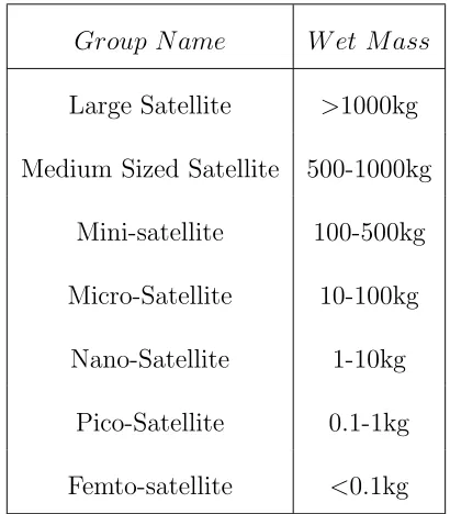
Many terms are used to describe this rediscovered class of satellites, including SmallSat, Cheapsat, MicroSat, MiniSat, NanoSat and even PicoSat and FemtoSat.
The US Defence Advanced Research Projects Agency refers to these as LightSats,
the U.S. Naval Space Command as SPINSat’s (Single Purpose Inexpensive Satellite
been generally adopted. The boundaries of these classes are an indication of where
launcher or cost tradeoffs are typically made, which is also why the mass is defined
including fuel [6]. Table 1.1 shows the classification of satellites on the basis of their wet mass (mass including fuel).
Small satellites have been used in a number of successful space missions. One of the major developments in the history of small satellites is the evolution of the
Cubesat kit. The Cubesat kit is designed to help the user to complete a successful
small satellite mission in as short of time as possible and at low cost [7]. It has been used to accomplish a number of successful space missions. On June 9, 2007, the Space
and Systems Development Laboratory (Department of Aeronautics and Astronautics
at Stanford University) successfully launched their third BioLaunch mission, B07C using the Cubesat kit [8]. On May 21, 2007, Kysat completed the first integration
of its CubeSat Kit-based KySat1 nanosatellite, and verified its target mass of under
1kg [1]. All of these and many more successful experiments show that the Cubesat kit has been proven to provide inexpensive and timely access to space for small payloads.
Table 1.1: Satellite Classification on the basis of weight
Group N ame W et M ass Large Satellite >1000kg Medium Sized Satellite 500-1000kg
Mini-satellite 100-500kg
Micro-Satellite 10-100kg
Nano-Satellite 1-10kg
Pico-Satellite 0.1-1kg
All satellites have one or more controllers which control the operation of the
satellite. They collect the data measured by the satellite, process it and send it
to the ground station. At the same time, they receive commands from the ground station and perform the required tasks. The controlling element can be considered
as the heart of any space based vehicle. It is a piece of hardware which can house
a number of algorithms targeted to perform a wide variety of tasks. The Cubesat kit consists of a Flight Model (10cm x 10cm x 10cm) which has a RISC-MCU-based
FM430 Flight Module as the main controlling element. There is also a provision for
plugging in other modules which can be used to perform a number of tasks like power supply and heath management [7].
From the view point of an electrical engineer, one of the main challenges in the field of space science is the mapping of complex control algorithms onto appropriate
hard-ware architectures. There is a wide knowledge gap between the team which designs
these algorithms and the team which implements the algorithms. There is a variety of hardware architectures available commercially onto which the algorithms can be
mapped. There also exist different design tools which can be used to perform the
implementation of these complex algorithms on appropriate hardware architectures. Although the tools speed up the design process, they often prove to be inefficient.
With the availability of a large suite of architectures and design tools, the design
engineer often gets puzzled in selecting the correct architecture and tools to perform
the implementation of the algorithm in an optimal manner.
There are a number of requirements which have to be met while implementing
an algorithm on particular hardware architecture. These requirements depend upon the application for which the implementation is targeted. In the case of designs for
small satellites, some of these requirements are a) The design should be able to meet real time constraints b) The design should have minimum power dissipation c) The
design should be reconfigurable, and d) The design should be small in size.
algo-rithms for small satellites. The methodology starts with the identification of the
candidate hardware architectures for implementing the algorithm. After selecting
ap-propriate hardware architecture(s), it provides a directed flow with decision making at several stages, and ultimately leads to a final design that meets all the
require-ments. The methodology will be validated by applying it to the complex Attitude
Determination and Control [1] algorithm designed for the attitude control of small satellites.
1.1
Motivation
As the utility of satellites grows from a strictly military and scientific venture to a vital component of large industries such as telecommunications, a greater number
of organizations are looking at available Earth-to-Orbit (ETO) launch vehicles. The
strong desire to reduce launch costs and, thereby, increase access to space has spawned a number of studies to advance the field of aerospace technology [9]. A wide variety of
algorithms are being designed for performing different tasks by the satellites in space.
One of the common categories of space based algorithms is that of the Attitude
Control algorithms. The attitude control algorithms are the algorithms that receive input from the sensors and calculate the appropriate actuator commands. These
commands, whether for reaction wheels, jets, or other actuators, are intended to
apply forces and torques to rotate or translate the spacecraft to the desired attitude. The attitude data, which is processed by the algorithms, comes from the attitude
sensors, for example gyroscopes, sun sensors, rotary encoders or star trackers. The
algorithm can be a very simple proportional control or a complex nonlinear estimator or many types in-between, depending on the mission requirements.
One such algorithm has been designed by the AMAS Laboratory at the Mechanical
and Aerospace Engineering Department at the University of Florida, Gainesville.
The algorithm has been developed to enable small satellites to perform autonomous
in Figure 1.1. It is the controller in Figure 1.1 which houses the attitude control algorithm. Here IMU refers to Inertial Measurement Unit, a sensor placed at the center of mass of the system shown below.
Figure 1.1: Attitude Determination and Control system designed by AMAS
The task of implementing this algorithm on hardware architecture has been
under-taken by the HiperDSP Laboratory at the North Carolina State University, Raleigh.
In the process of trying to implement the algorithm, it was realized that there was a
need for a directed methodology which can guide a design engineer in taking the right decisions at all the levels starting from the selection of the right hardware architecture
The type of hardware architectures that the control algorithms can be mapped
onto are General Purpose Processors (GPP), Digital Signal Processors (DSP), Field
Programmable Gate Arrays (FPGA), Application Specific Instruction-Set Proces-sors (ASIP), Reconfigurable ProcesProces-sors and Application Specific Integrated Circuits
(ASIC) [10]. There are various suites of tools available for performing
implementa-tions on each of these architectures. The choice of the right set of tools is essential in any development process. It has been observed that tools from different vendors,
which are part of a single development flow, may not be compatible with each other.
It has also been observed that the same tool works well for one application model but does not work well for the other.
All the above factors lead to the idea of developing a methodology for implement-ing complex control algorithms on appropriate hardware architectures. The
method-ology which is described in this thesis can not only be used to analyze the Attitude
Determination and Control [1] algorithm, but a number of other algorithms being developed at the AMAS Laboratory.
1.2
Related Work
A number of design based methodologies have been developed for various
ap-plications. All the methodologies start their flow with the Platform Independent
Model [11] of the system. Using the commercially available tools, they analyze the complexity of the algorithms and take the decision regarding the architecture on which
the algorithm can be implemented and the tools which can be used to implement the
algorithms on the selected architectures. Some of the methodologies that have been developed so far are listed below:
• An Efficient Methodology for Design and Verification of Software Defined Ra-dio [12]
three main steps. The flow, leading from system specifications down to
imple-mentation, goes across multiple abstraction levels. The first step is to build
a platform independent model of the system. Next the model goes through the partitioning process to generate the Platform Specific Model. This
Plat-form Specific model is then refined down to the RTL level for integration on
the target board. The preliminary modeling and design of the system is done using Simulink from Mathworks. After the process of partitioning is carried
out, the hardware part is implemented using VHDL and the software part is
implemented using C/C++. The target board consists of FPGA and CPU core.
• True DSP Synthesis [13]
In this methodology, a Register Transfer Level (RTL) implementation of the
algorithm is done automatically from the high level description of the algorithm.
It is targeted mainly for DSP designs. It assumes that the implementation of the algorithm is being done on the FPGAs or the ASICs.
• Mimosys Design Flow [14]
In this design flow, the starting point is the C code of the application model. This C code is profiled by the inbuilt profiler of the tool. The profiling results
identify the hardware accelerator components. After the components are iden-tified, it generates the VHDL code for the hardware accelerators and modifies
the original source code to make use of the newly generated hardware
accelera-tor components. The modified source code and the HDL components are then
imported to Xilinx Platform Studio [15] for the purpose of implementation on the FPGA.
Apart from the methodologies listed above, a number of other methodologies have
been developed to implement algorithms on different hardware architectures. One of the main drawbacks of these methodologies is that they use certain tools which are
not readily available. For example, one hardware-software codesign methodology
[18]. GAUT is a high level synthesis tool for the ASICs and SYNDEX produces
the dedicated code for the DSPs. These are the tools which are developed for the
purpose of research and are not commercially available. Moreover, the methodologies that have been developed so far are targeted to specific class of applications and have
been devised keeping in mind those specific applications. They cannot be applied to
all the applications. All the above drawbacks lead to the process of development of a methodology for analyzing complex algorithms.
1.3
Contribution
The following thesis presents a methodology for analyzing complex control algo-rithms for small satellites. It starts with the selection of the right hardware
archi-tecture(s) and provides a directed flow involving decision making at several steps in
order to reach a final conclusion. The methodology assumes that the given applica-tion model has been designed in Simulink by M athworksr. An important decision making point in the methodology is whether to manually write the software
descrip-tion of the model or to use commercially available tools for the same purpose. A
simple case study of an FIR filter is carried out to obtain a conclusion regarding the above mentioned point. The case study also describes the different
optimiza-tion techniques that can be performed on the software descripoptimiza-tion of a model. The
proposed methodology is validated by applying it to the Attitude Determination and Control algorithm designed for the attitude control of small satellites. The complexity
analysis of the algorithm is carried out using the Time Complexity Analysis method
described in the methodology. This analysis leads to the identification of two critical modules from the algorithm : Matrix Multiplication and LU decomposition of a
ma-trix. As directed by the methodology, software implementations of these algorithms
are performed. These implementations are optimized using a number of techniques like Forward Store Optimization and Loop Unrolling. These optimized software
mod-els are compared with the hardware modmod-els built at the RTL Level of Abstraction.
to Market. After analyzing the results, a decision is made regarding the best way to
implement the algorithm.
1.4
Thesis Organization
The thesis is organized in the following way:
Chapter 2 provides a description of the Design Space Exploration. It discusses the
different hardware architectures with their important features. It also gives a brief idea about the various factors to be taken into consideration while choosing the right
hardware architecture for a given application. Chapter 3 describes the design
method-ology for analyzing complex algorithms in detail. The reader is made familiar with the concept using lucid flow diagrams. Chapter 4 describes the case study of the FIR
filter which shows comparison between tool generated and hand written C codes.
It also describes the different kinds of optimizations that can be performed on the software description of a model to improve its performance. This case study forms
the foundation of one of the important decision making points in the methodology
described in Chapter 3. Chapter 5 deals with applying the methodology to the
Atti-tude Determination and Control algorithm. The first part of the chapter gives a brief overview of the ADC algorithm. The next part describes the detailed analysis of the
algorithm using the proposed methodology, and the final part gives a conclusion on
the basis of the results obtained by analyzing the algorithm. Finally in Chapter 6, we conclude our work by giving an overview of our contribution and providing details
Chapter 2
Design Space Exploration
The ever increasing complexity of signal processing and control algorithms has lead to the need for development of different methodologies to implement algorithms
efficiently within a design cycle that is ever shrinking. The path from algorithm
de-velopment to the actual implementation is a long process and needs careful decision making at various levels of abstraction in order to have a design which is an
improve-ment over existing designs. The most important step in impleimprove-menting an algorithm
is choosing the right hardware platform onto which the algorithm can be mapped.
This can be based on design specifications and requirements of the specific applica-tions. The choice of the correct hardware architecture depends upon a number of
important parameters, e.g., Time to Market, Cost, Performance, Power Consump-tionandFeature Flexibility[10]. After the choice of the correct hardware architecture, the next step is to select the correct methodology for design and implementation of
the algorithm onto the selected hardware architecture. Currently, most designs are
accomplished through the use of HDL-centric flows. However, device densities have increased at a pace that such flows have become both cumbersome and outdated.
The need for a more innovative and higher-level design flow that directly
ap-plication based on several factors, and also on the different kind of high level design
methodologies generally used to go from algorithm to design and implementation.
2.1
Choice of Hardware Architecture
There are numbers of factors which affect the selection of the correct hardware
architecture for a specific application. For a space based application, these factors
are Time to Launch, Performance, Power Dissipation, Price and Feature Flexibility. This section discusses the importance of each and every factor along with the tradeoffs
between them.
2.1.1
Time to Launch
In the language of an aerospace engineer, the process of designing, fabricating and
demonstating the flight capabilities of a space based system is referred to as Design Build and Fly, abbreviated as DBF. The total time required to perform all these activities is referred to as Time to Launch. A significant amount of the total time is
spent in the design process. The greatest threats to the field of aerospace engineering
are technological obsolescence and ever intensifying global competition. In order to cope up with these threats, one of the main goals of the design team should be to
shrink the design and development cycles.
2.1.2
Performance
Performance is an important criterion for space based applications, as the design
should be able to meet the real time space constraints. Performance may be measured
in many ways, but generically we look at millions of operations per second (MIPS), millions of multiply accumulates per second (MMACS), or, sometimes, the more
priority basis only when other key requirements such as low power or low cost increase
in priority [10].
2.1.3
Price
Price includes the design costs and the Non Recurring Engineering (NRE) costs.
A clear understanding of design costs can be indicated by giving an example of
hard-ware and softhard-ware designs. Softhard-ware design involves describing an algorithm using some high level languages like C and C++. Hardware design involves describing the
algorithms using hardware descriptive languages like VHDL and Verilog. The design
has to be carried out such that the HDL description can be synthesized to produce the gate level netlist which can be mapped onto a hardware device. All this requires
highly skilled engineers. The cost of the tools involved in the design process also
adds to the total design cost. According to the International Technology Roadmap for Semiconductors (ITRS) 2003 edition, the NRE costs, including both design and
manufacturing costs, in the deep submicron era, can easily amount to tens of millions
of dollars [20] [21]. So, price is often the most obvious criteria of priority.
2.1.4
Power Dissipation
The most important requirement for any space based design is that it should
have low power dissipation. Since the beginning of the 1990s, the reduction of power dissipation has become more and more important in chip design [22]. In addition to
costly heat removal expense, excessive power consumption in systems also reduces the
battery lifetime. As a result, the quality and reliability of a system would be severely compromised by high power dissipation. So, one of the main motives of all the design
engineers is to develop new design techniques which can lead to the minimization of
power dissipation in all types of applications. Not only the design technique, but also the architecture on which the design is implemented, plays a vital role in determining
2.1.5
Feature Flexibility
Feature flexibility is the capability to modify or add features to meet changing requirements. Requirement changes occur more and more rapidly in today’s markets.
For example, early entry into standards-based products (such as communications or
compression standards) before the standards are solidified is critical if manufacturers are to lead in the market. However, designers must build future proof products that
can be upgraded to reflect the final standard after all nuances have been worked out.
Thus you must have the feature flexibility required to update your product easily and quickly after market [10].
Feature flexibility is quite important for space based applications. A space satellite may be configured to perform a particular task, but it is possible that the task may
have to be modified or replaced by another task in the future. The main factor to
be taken into consideration for designing space based systems is that the hardware device for such systems should be reconfigurable and evolvable.
2.2
Architecture Exploration
The key requirements for an architecture to implement a complex signal process-ing or control algorithm are high performance, flexibility and energy efficiency. A
recent Texas Instruments survey indicated that of the signal processing architectures
considered by today’s developer, the following alternatives were the most popular: ASIC, ASSP, configurable processor, DSP, FPGA, MCU and RISC/GPP [10]. Out
of these architectures, the four most commonly used architectures are GPP, DSP,
FPGA and ASIC. Programmable DSP architectures are flexible, but inefficient. Ap-plication Specific Integrated circuits (ASICs) are efficient, but inflexible. FPGAs
make a tradeoff between ASIC and DSP by limiting their flexibility to a
particu-lar domain [20]. This section gives brief information about these architectures along with the advantages and disadvantages of using them for a particular application with
2.2.1
General Purpose Processors (GPP/RISC)
General Purpose processors are programmable processors that can utilize software programmability to perform a wide variety of functions and hence have the greatest
amount of flexilibility. Their core architectures are not designed and optimized to
per-form a specific application. As a result of this, these processors are the least efficient of all the hardware architectures. They are judged fair in terms of Price and Power [10].
An example of a General Purpose Processor is an ARM Processor. An improvement
to the class of general purpose processors is the developement of Application Specific Instruction-set processors (ASIP) whose core’s architecture and instruction set are
customized in order to increase efficiency and reduce power dissipation [23].
2.2.2
Digital Signal Processors (DSP)
Digital Signal Processors are specialized microcomputers for real-time signal
pro-cessing applications. Because of their specialized applications, programmable DSPs
have evolved architectures that are significantly different from conventional micropro-cessors. On certain DSP benchmarks, their performance has consistently exceeded
that of microprocessors with arithmetic co-processors by more than the order of
mag-nitude throughout their ten year history [24].
A number of architectural innovations have been used to achieve this impressive
performance. The most basic is the integration of fast multiplier/accumulator hard-ware into the data path; the arithmetic is not done on a processor which is separated
from the main data path, but rather is an integral part of execution of every
instruc-tion. They have Harvard architecture with separate data and program buses with for the individual data and program memories respectively. They are referred to as
first generation DSPs. The second generation DSPs retain much of the design of the
first generation, but with added features such pipelining, multiple arithmetic logic units (ALUs) and accumulators to enhance performance. TMS320C20 from Texas
A further enhancement was observed with the evolution of the third generation
DSPs. These DSPs have capabilities of executing Single Instruction Multiple Data
(SIMD), Very Long Instruction Word (VLIW) and Superscalar operations. SIMD allows one instruction to be executed on many independent groups of data. For SIMD
to be effective, programs and data sets must be tailored for data parallel processing,
and SIMD is most effective with large blocks of data. VLIW processors issue a large number of instructions either as one large instruction or in a fixed instruction packet,
and the scheduling of these instructions is performed by the compiler. Superscalar
processors, on the other hand, can issue varying number of instructions per cycle and can be scheduled statically by the compiler or dynamically by the processor itself [25].
A further enhancement is observed in the latest TI TMS320C4x processors which
combine both VLIW and SIMD into their architecture known as VelociTI.2. All
these specialized architectures make DSPs faster and more power efficient than the General Purpose Processors.
2.2.3
Field Programmable Gate Arrays (FPGA)
FPGAs are integrated circuits that have undefined function at the time of
man-ufacturing and must be programmed before it can be used. An FPGA is comprised
of a two dimensional array of configurable logic blocks (CLB), which are connected by a configurable matrix of wire switches. Basic building blocks, such as adders and
shifters, can be formed by configuring logic cells and interconnecting them. These
basic building blocks can be used to form more complex designs.
The behavior of FPGA is specified using either a hardware description language or
a schematic that is designed by Electronic Design Automation (EDA) tools. Design Automation tools are used to synthesize a HDL or schematic description to a netlist
of logic cells for a target FPGA technology. Placement and Routing automation tools
are used to allocate the logic cells in the FPGA device and the connections among these logic cells [20] [26]. FPGAs can achieve high performance and are quite efficient
good in terms of Time to Market and Feature Flexibility and fair in terms of Price
and Power efficiency [10].
2.2.4
Application Specific Integrated Circuits (ASIC)
ASICs are manufactured on silicon wafers that can hold hundreds of silicon chips,
which are called dies. They are developed using silicon compilers that can translate an
HDL into a gate level netlist. ASICs can be made either from standard cell libraries or can be have full custom design. The full custom design will be more energy-efficient,
but is very labor intensive [20].
ASICs represent the most efficient solution to implement a particular algorithm in
hardware in terms of performance, area, and energy efficiency. The major drawback is their inflexibility. Once the ASIC is manufactured, its function cannot be changed.
The Time to Market for an ASIC is high as compared to other architectures. A small
modification requires developing a new ASIC.
Table 2.1 summarizes the characteristics of all the architectures with respect to the criteria discussed in Section 2.1
Table 2.1: Architectures and their Characteristics
T ime to M arket
P erf ormance P rice P ower F eature F lexibility
GPP/RISC Good Good Fair Fair Excellent
DSP Excellent Excellent Good Good Excellent
FPGA Good Excellent Fair Fair Good
The most important trade-off is between flexibility and efficiency as illustrated
by Figure2.1. Flexibility dictates design costs, time to market and reconfigurability, while efficiency determines performance and power dissipation. The figures of merit for measuring efficiency are MOPS/mW (Energy Efficiency) and MOPS/mm2
(Area
Efficiency), where MOPS is defined as Millions of Algorithmically defined Arithmetic
Operations (e.g. multiply, add, shift) [2].
On one end of the spectrum are ASICs. They are specialized to a given
applica-tion. Therefore, they have the least flexibility compared with other architectures. The lack of flexibility introduces high NRE costs, and a prolonged and expensive design
flow. However, due to specialization, the efficiency is highest in terms of power and
performance. On the other end of the spectrum are general purpose processors like Intel’s Pentium 4. They can be organized and sequenced to implement arbitrary
com-putations. This level of flexibility brings high-level programming language support,
zero manufacturing and low design NRE cost for the application developer. However, they are too inefficient to deliver high performance and low power when applications
have much parallelism [27]. Between these two extremes, architectures like DSP and
FPGA try to make different compromises between efficiency and flexibility.
2.3
Implementation Techniques
This section discusses the three basic implementation techniques used commonly for mapping complex algorithms onto appropriate hardware architectures. Today’s
VLSI technology allows companies to build large, complex systems containing millions
of transistors on a single chip. To exploit this technology, designers need sophisticated CAD tools that enable them to manage millions of transistors efficiently [4]. Until
now, designers have been doing the design process at lower levels of abstraction like the
Figure 2.1: Flexibility vs. Efficiency Tradeoff [2]
the overall productivity of the design. The solution to this is to move up to the higher
levels of abstraction. The advantage of this new methodology is that it allows us to design in a purely behavioral form, devoid of implementation details and then to map
the design onto appropriate hardware architectures using the commercially available
CAD tools.
In order to describe the design at the behavioral level, we need a tool which
allows us to design and simulate the algorithm at the block level. Simulink is a software package for creating, editing and simulating dynamical systems on Matlab
models where models are created as block diagrams. It also allows complete models
to be simulated by a variety of integration solvers. In addition, users can change
parameters and immediately see what happens for “what if” exploration. While the simulation is running, users can see the result via display blocks, such as scopes. Based
on the assumption that the high level description of the algorithm has been done in
Simulink, the types of implementation can be divided into three main categories:
• Software Only Implementation
• Hardware Only Implementation
• Hardware-Software Co design
2.3.1
Software Only Implementation
In this type of implementation, the Simulink algorithm is converted into C code
and compiled to produce the binary code which can be run on a Digital Signal
Pro-cessor (DSP). The algorithm is converted to C code using the Real Time Workshop provided by Mathworks. Real-Time Workshop is a toolbox that is part of the
Mat-lab Simulink package. It allows C code to be generated from block diagrams in
Simulink. Once a system has been designed and simulated in Simulink, code for dig-ital signal processors can be generated, compiled, linked, and downloaded to a DSP
board [29] [30]. The process of generating C code from a Simulink model can be
illustrated with the help of the flow diagram shown in Figure 2.2.
Real-Time Workshop converts the Simulink model stored in the .mdl file into .rtw
file. This file contains all the necessary information about the Simulink model that is needed during code generation process. RTW also generates makefile (model.mk)
from the system template makefile (system.tmf). After that, the Target Language
Compiler (TLC) is invoked into the code generation process and it converts Simulink model to the C code. When the TLC concludes with the C code generation process,
! !
!" #
Figure 2.2: Code Generation Process from Simulink Model [3]
appropriate compiler, generates executable code. This code can be imported to a tool specific to the target DSP. An example of one such tool is the TI Code Composer
Studio. The compiler present in this tool can be used to generate assembly code
2.3.2
Hardware Only Implementation
In this type of implementation, the concept of high level synthesis is used. High-level synthesis is a sequence of tasks that transforms a behavioral representation into
an RTL design. The design consists of functional units such as ALUs and multipliers,
storage units such as memories and register files, and interconnection units such as multiplexers and buses. The block diagram in Figure 2.3 illustrates the flow of high level synthesis.
The compiler converts the behavioral description into an internal representation.
The RTL library contains the physical and simulation models of components to be
used during synthesis. The netlister generates the final RTL structure, consisting of a netlist of RTL components and a simulation model of each component. To verify
the synthesized design’s correctness, the designer can simulate the input description
and the generated netlist by means of the simulation environment, an adjunct to the high-level synthesis system [4].
Xilinx System Generator and Simulink HDL coder are commercially available tools which facilitate the behavioral description and simulation of complex designs.
Both the tools can be used to perform design at a level of abstraction higher than
the RTL level. The design implementation using these tools is faithful in that the system model and hardware implementation are bit-identical and cycle-identical at
sample times defined in Simulink. In System Generator, the capabilities of IP blocks
have been extended transparently and automatically to fit gracefully into a system level framework. User-defined IP blocks can be incorporated into a System Generator
model as black boxes which will be embedded by the tool into the HDL
implemen-tation of the design [31]. However, there exists no way to generate hardware from models which use the basic Simulink Blockset, and as such, greatly restricts the
Figure 2.3: A generic high level synthesis system [4]
2.3.3
Hardware-Software Co-Design
Whenever we want to have a fast implementation of an algorithm, the best method is to have a software only implementation. The design time for this particular
efficient implementation of the algorithm. On the other hand, when Time to Market
is not an important factor, one should go for Hardware only Implementation. The
design time will be high but at the same time, the performance will be excellent. An intermediate between these two is the methodology of hardware-software codesign. It
has advantages of both the methodologies.
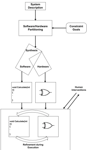
Hardware-Software co-design, known as CoDesign methodology, takes into account
the features of software and hardware elements in a unique design process. Some
criteria are needed to split the system under development into hardware and software parts. The usual constraints are performances, hardware area or cost criteria. This
process is usually called the “partitioning process”. After that, the software has to
be compiled on the target architecture, and then the hardware has to be synthesized. A software and hardware evaluation is made to see if the performances and area
requirements are reached. If not, the partition needs to be revised. The global
scheme for hardware-software Codesign methodology is illustrated in Figure 2.4. The first step in hardware-software partitioning is a profiling step to evaluate the
relative computational complexities for the different blocks in the algorithm. Tasks which contribute to a large portion of the execution time of the processor are natural
candidates for hardware implementation [32]. Profiling can be done using a number
of profilers like the GNU gprof GCC profiler and the profiler in TI Code Composer Studio. The profilers can be used to give the execution times of the individual
func-tions of the code. From the profiling results, the bottlenecks can be identified for
implementation in hardware. In this manner, the performance of the overall system
!
!
" #$
%
Chapter 3
Design Methodology
The main goal of this research is to develop a methodology that can assist a system engineer in implementing a complex algorithm on appropriate hardware architecture.
The methodology described in this section is a step by step process which when
applied to an algorithm, gives a clear understanding of the process of implementation of the algorithm. The validity of the methodology is shown by applying it to the
Attitude Determination and Control [1] algorithm designed for the attitude control
of small satellites.
Some of the architectures used for real time signal processing and control
ap-plications are General Purpose Processor (GPP), Digital signal Processor (DSP), Field Programmable Gate Array (FPGA), Application Specific Integrated Circuits
(ASICs), Application Specific Instruction-set Processor and Reconfigurable
Proces-sor [10]. Out of these, the four most commonly used architectures for majority of applications are GPP, DSP, FPGA and ASIC. The algorithm can be implemented
on any of these architectures. This methodology shows the process of analyzing the
algorithm and deciding the platform(s) on which the algorithm can be implemented.
designed and simulated using Simulink from MathWorks. The entire flow is divided
into six main steps. The steps descibed in the methodology are specific to TI DSPs
and Xilinx FPGAs. The reasons for choosing TI and Xilinx devices are listed below:
• Both TI and Xilinx provide state-of-the-art technology devices. The latest TI DSP TMS320C67xx series has the VelociTi architecture which is a combination
of both VLIW (Very Long Instruction Word) and SIMD (Single Instruction
Multiple Data) architectures. The Virtex-4sx FPGA from Xilinx is best suited
for DSP and low power applications.
• There are robust tools associated with these devices which enable fast and
efficient implementations of designs on these device architectures.
• It is assumed that the algorithms are designed and simulated using Simulink from Mathworks. Both TI and Xilinx have tools which are compatible with the
toolboxes present in the Matlab Simulink package.
Each and every step of the methodology will be explained in detail with use of
ex-amples to enhance the understanding of the process. The methodology assumes that the design engineer has a good knowledge of software (C) and hardware descriptive
(Verilog / VHDL) languages. A number of steps in the process involve the use of some
commercially available tools like Xilinx ISE [33] and TI Code Composer Studio [34]. The engineer is not expected to know the functionality of the tools. A brief overview
of the tools will be provided when they are referred to in the methodology.
The flow described involves a comparison of hardware and software
implementa-tions. The comparison is on the basis of three important factors: Execution Time
(Speed), Power Dissipation, and Development Time (a part of the total Time to Launch for space based applications). Another factor which is of significance for
space based applications is the size (area) of the design. It is also touched upon in
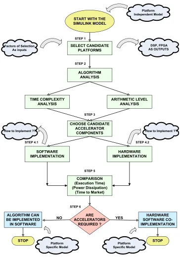
Figure 3.1 shows the major steps of our design methodology. A detailed description of all the steps is given in the section below.
3.1
Proposed Methodology
Step 1: Selection of the candidate platforms (architectures)
The first step in the methodology is to narrow the selection of platforms that canbe chosen as candidates for algorithm implementation. The Simulink model of the
algorithm at this stage is a general description of the algorithm irrespective of the platform on which it can be implemented; hence it is called Platform Independent
Model (PIM). We present a simple technique which helps to select the right
architec-ture(s) based on the requirements of the application. This technique is based on data provided by Texas Instruments. The choice of appropriate architecture(s) depends
upon criteria like Performance, Power Dissipation, Cost, Time to Market and Feature
Flexibility.
This methodology focusses on algorithms for space based applications in which
the most important criterion is low power dissipation. Other criteria like Performance and Development Time are also fairly important. Let us consider that weights are
given to these criteria on the basis of requirements of the application. The weights are between 0 and 1. 0 means no importance and 1 means most important. We take
four criteria into consideration: Performance, Power Dissipation, Development Time
and Flexibility. Let the weights given to these criteria be the inputs of a system which
! ! " # $ $ % & % % ' %
( ) " ! ! *
( + ! ! ! *
( ! , *
+ -- +
--.
-$
/ % 0
!! !! 1 2 3 451 452 6 7
Figure 3.1: Overall flow diagram of the Proposed Methodology
The input given to the system is a 4×1 matrix as shown below
W eight given to T ime to market = 0.6 W eight given to P erf ormance = 0.8 W eight given to P ower consumption = 1.0
W eight given to F lexibility = 0.4
Table 3.1: Characteristics and their numerical values
Characteristics N umerical V alue
Excellent 1
Very Good 0.8
Good 0.6
Fair 0.4
Poor 0.2
Table 3.2: Tabular representation of the system matrix derived from data from TI and Table 3.1
T ime to M arket P erf ormance P ower F eature F lexibility
GPP 0.6 0.6 0.4 1.0
DSP 1.0 0.8 0.6 1.0
FPGA 0.6 1.0 0.4 0.6
ASIC 0.2 1.0 0.6 0.2
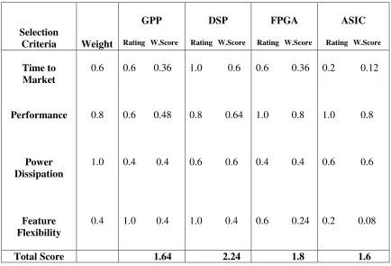
We use a technique, called Concept Scoring[35], to select the best architecture for the purpose of implementation. In this technique, the input weights are multipled by
the ratings given to each architecture to obtain weighted scores for all the criteria.
The total score for each architecture is obtained by adding the individual weighted scores for all the criteria. This can be seen in Figure 3.2. Here W.Score refers to the weighted scores obtained by multiplying the input weights with the ratings given to
each architecture.
Selection
Criteria Weight
GPP
Rating W.Score
DSP
Rating W.Score
FPGA
Rating W.Score
ASIC
Rating W.Score
Time to Market Performance Power Dissipation Feature Flexibility 0.6 0.8 1.0 0.4
0.6 0.36
0.6 0.48
0.4 0.4
1.0 0.4
1.0 0.6
0.8 0.64
0.6 0.6
1.0 0.4
0.6 0.36
1.0 0.8
0.4 0.4
0.6 0.24
0.2 0.12
1.0 0.8
0.6 0.6
0.2 0.08
Total Score 1.64 2.24 1.8 1.6
Figure 3.2: Concept Scoring Matrix
the scores for the four architectures GPP, DSP, FPGA and ASIC in that order. It can be seen that DSP has the highest score of all. This indicates that DSP is the ideal
candidate for implementing the algorithm. But as far as performance is concerned,
FPGA has higher performance than DSP. Also, it has the second highest weighted
score as observed from the data obtained. So, a clear decision cannot be taken as to which is the right architecture onto which the algorithm can be mapped. The solution
is to implement the computationally complex parts of the algorithm on FPGA and
the rest of the algorithm on DSP. The details regarding this aspect are discussed in the ensuing steps of the methodology.
The advantage of this technique is that it narrows down the window of selection
of the target architectures. GPP and ASIC have low weighted scores, so they are
Step 2: Algorithm Analysis
The second step in the methodology is to perform the analysis of the Simulink model provided. In the first step, it was deduced that DSP and FPGA are the
candi-date architectures on which the algorithm can be implemented. Since the performance
of FPGA (as seen in Table 3.2) is better than that of the DSP, it can be used to im-plement the complex parts of the algorithm, and DSP can be used to imim-plement the
rest of the algorithm. In order to determine the computationally complex parts of
the algorithm, the algorithm has to be analyzed.
To analyze an algorithm is to determine the amount of resources (such as time and
storage) necessary to execute it. Most algorithms are designed to work with inputs of arbitrary length. Usually the efficiency or complexity of an algorithm is stated
as a function relating the input length to the number of steps or storage locations.
Algorithm analysis is an important part of a broader computational complexity the-ory, which provides theoretical estimates for the resources needed by any algorithm
for solving a given computational problem. These estimates provide an insight into
directions for efficient implementation of algorithms.
The process of complexity analysis of an algorithm can be illustrated with the
help of the flow diagram in Figure 3.3. It has been deduced in Step 1 that DSP and FPGA are the candidates for implementing the algorithm. The following steps give a
brief overview of the complexity analysis process illustrated by the flowchart in Figure
3.3.
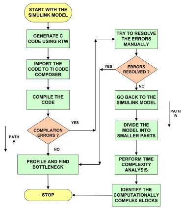
1. Use Real Time Workshop from Mathworks to generate C code from the Simulink
model. The process has been described in Section 2.3.1.
2. The next step is to import this C code into TI Code Composer. Select the target Digital Signal Processor for which the code needs to be compiled. This
Figure 3.3: Algorithm Analysis Flow
3. Compile the C code.
4. The next step is to see whether the compilation of the code gives any errors. The
code that is compiled is a tool generated code, so it is possible that this code
does not get compiled for all the compilers. Real Time Workshop generates the C code using certain standard MathWork libraries. These libraries may
code. These data structures are not recognized by the built-in compiler of Code
Composer Studio.
5. If there are no compilation errors, the next step is to profile the C code. This is denoted by Path A in the flow diagram. The Code Composer Studio Profiler
analyzes the execution of the C program and shows where the“hotspots”, or
the areas where a large portion of the cycles being used, occur. The profiler can show the developer how many cycles a function takes to execute, as well as
how often it is called.
6. If there are compilation errors, the next step is to resolve the errors. This depends upon the number and types of errors. In order to resolve the errors, it
is required to understand the C code generated by RTW.
7. If the code generated by RTW is difficult to understand, and the errors cannot be resolved, the next step is to analyze the algorithm using the divide and
conquer method. This is denoted by Path B in the flow diagram. Divide and
conquer is a technique for analyzing algorithms that consists of dividing the
problem into smaller sub-problems which are identical to the original problem but smaller in size, and then analyzing the sub-problems independently of each
other.
8. If Path B is chosen, the last step is to find out the computationally complex blocks from the model using Time Complexity Analysis. An overview of Time
Complexity Analysis is presented below.
Time Complexity can be defined as a measure of the amount of time required to
execute an algorithm. It gives an approximate estimate of the number of operations needed to complete the computation of the given algorithm. It is independent of
the programming language chosen to implement the algorithm, the quality of the
This gives an upper bound on the amount of work done for sufficiently large n. The
following examples illustrate the method of determining the Time Complexity of an
algorithm.
Example 1: Matrix Addition
Consider the addition of two matrices A and B of m rows and n columns using the
following algorithm.
Procedure: MATADD (A, B: matrix; var C: matrix); Begin
f or i=1:m do f or j=1:n do
C[i,j] = A[i,j] + B[i,j];
End
In this algorithm, we need
• m x n additions
• 2 x m x n memory reads
• m x n memory writes
Thus the time complexity of the procedure matrix addition is (t1 x m x n) + (t2 x 2 xm x n) + (t3 xm x n)
= (m x n) (t1 + 2t2 + t3) = O(m x n)
where,
Example 2: Polynomial Evaluation
Consider the polynomial
p(x) =anx n
+an−1x
n−1
+an−2x
n−2
+...+a2x 2
+a1x+a0 where an is non-zero for all n >= 0
The first term in the polynomial requires n multiplications. The second term re-quires (n-1) multiplications. The third term rere-quires (n-2) multiplications. Likewise,
the third last term requires 2 multiplications and the second last term requires a
single multiplication. The total number of multiplications required is given as
T(n) = (n) + (n−1) + (n−2) +...+ 2 + 1 =n(n+ 1)/2
=n2
/2 +n/2
This is an exact formula for the maximum number of multiplications. We say that
the number of multiplications is on the order of n2
, or O(n2
). The following table
shows the different categories of Time Complexities.
Step 3: Choose Candidate Accelerator Components
As illustrated in the flow diagram of Figure3.3, there are two different paths (A or B) which can be taken to perform the complexity analysis of the algorithm. This step
of the methodology discusses about selection of the candidate accelerator components
from the results of the complexity analysis. This section is divided into two parts. Part A describes the method of selecting the accelerator components when Path A
Table 3.3: Different Categories of Time Complexities
O() Category
O(1) Constant Time Algorithm
O(logN) Logarithmic Time Algorithm
O(N) Linear Time Algorithm
O(NlogN) Linearithmic Time Algorithm O(Na
) a>1 and a is an integer Polynomial Time Algorithm
O(bN
) b>1 and b is a real number Exponential Time Algorithm
Part A
This part discusses the method of selecting the candidate accelerator components
using the profiling results generated by the Code Composer Studio profiler. Let us consider that the C code of the model consists of six functions. The profiler gives
information in terms of the number of target processor clock cycles required by all the
functions to process certain amount of input data. Suppose the functions in the C code of the model are f1 through f6, and the number of processor clock cycles required
to process 10 samples of input data by each function are 10, 200, 5000, 250, 300 and
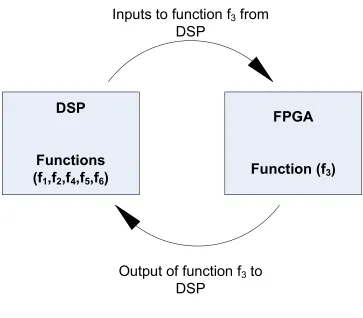
1000 in that order, then, it can be seen that the function f3 consumes maximum number of clock cycles. In other words, it is the ”hotspot” of the C code. The
conclusion is that this function is the candidate accelerator component and can be
implemented in hardware on FPGA and all the other functions can be implemented in software on DSP. This is shown in Figure3.4. The arrows indicate the flow of data between DSP and FPGA.
Part B
This part discusses the method of selecting the candidate hardware accelerator
Figure 3.4: Flow of data between DSP and FPGA
dividing the Simulink model into small parts and then analyzing each one of them
individually. Each and every Simulink block in the small model can be treated as an algorithm by itself. Consider the model shown in Figure 3.5.
It has adders, multiplexers, matrix concatenation blocks and a matrix addition
block. Each and every block in this model can be considered as an separate algorithm
and its time complexity can be determined individually. The time complexity of an
adder is O(n). Matrix concatenation is a constant time block as it simply involves concatenation of elements which does not involve any mathematical operations. The
most critical block in this model is the matrix addition block. This block adds two
2×2 matrices. This block has a time complexity of O(n2
)(as shown in the example in the previous section where m=n)where n = 2 in this case. Hence the block which
Figure 3.5: A simple Simulink model to explain the concept of Time Complexity Analysis
addition. The following set of rules is used to compare the complexities of the various blocks.
• n dominateslog2(n) • nlog2(n) dominates n
• n2
dominates nlog2(n)
• nm
dominates nk
when m >k • an
dominates nm
That is, log2(n) <n <nlog2(n) < n2
<... < nm
< an
for a>= 1 and m> 2
In this manner, the blocks with maximum time complexity are chosen as the
can-didate accelerator components. This operation is performed on all the small models
obtained by dividing the large Simulink model.
Step 4: Perform Software
\
Hardware Implementations of
Ac-celerator Components
This step involves performing software and hardware implementations of the
ac-celerator components selected in Step 3. Both the software and hardware implemen-tations can be done in two different ways. This step has been divided into two parts.
Step 4.1 gives details of the software implementation and Step 4.2 gives details of the
hardware implementation.
Step 4.1: Software Implementation
The basic aim of performing the software implementation of the accelerator
com-ponents is to compare its performance with its hardware implementation. The overall process of software implementation of the candidate accelerator components is
illus-trated in the Figure 3.6. What follows is a brief overview of all the blocks.
The software implementation of the accelerator components can be done in two
different ways. This choice depends upon the path taken by the designer in Step
2. If path A is taken (which identifies the accelerators on the basis of the Code Composer profiling results), the designer should choose option 1 in Figure3.6. On the other hand, if path B is taken in step 2 (which identifies the accelerators using Time
Complexity Analysis), the designer should choose option 2 in Figure 3.6. A detailed analysis of the comparison between option 1 and option 2 in terms of performance of
the C code will be shown in Chapter 4. After generating C code for the accelerator
!
" # #
"
Figure 3.6: Software Implemenation Process
Studio profiler. Then, the number of processor clock cycles required to execute the code for particular input data is observed. The next step is to optimize the C code
to improve its performance.
of clock cycles required to execute the code. One of the disadvantages of C compilers
in taking full advantage of high-performance DSP architectures is that they cannot
always efficiently map complex algorithms to the multiple VLIW functional units. In order to overcome this limitation of the compilers, the designer has to modify
the C code in such a manner that the resulting assembly code generated by the
compiler can take maximum advantage of the underlying architecture. This can be done by performing different optimizations on the C code like Loop Unrolling [36],
Forward Store Optimization [37] and use of intrinsic functions. These techniques will
be explained in detail in Chapter 4 with the help of a case study.
After performing optimizations on the C code, it is again compiled and profiled to
observe the improvement in performance. This process is repeated several times till we reach the point where performing any optimization does not improve the performance
of the code any more. The optimized code which takes the least number of processor
clock cycles to process a particular set of input data is chosen as the standard for comparison with hardware implementation.
Step 4.2: Hardware Implementation
After performing the software implementation of the accelerators, the next step is to do their hardware implementation on an FPGA. The hardware implementation
process takes more time than the software implementation process and requires careful
consideration at each step in order to have an efficient design. The flow diagram in
Figure 3.7 illustrates the main steps in the hardware implementation of a design. This flow can be used to perform implementation of designs on Xilinx FPGAs.
Like the software implementation, the hardware implementation of the accelerator
components can be done in two different ways. The first option is to use Xilinx System Generator [31] to perform block level design of the accelerator. A brief overview of
Xilinx System Generator has been given in Chapter 2. The advantage of using System
! " #$% #&
'
#$% #& (
! "
) * +
)
%
,
$ - "
. ) "
/" "
% 0
Figure 3.7: Hardware Implemenation Process
disadvantages. One might view System Generator as a high-level design tool in which high-level function blocks are connected together while the tool handles the remaining
details. This view is inconsistent with our experience. While the design entry method
is high-level, the designs themselves typically are not. First of all, it does not have blocks corresponding to all the Simulink blocks in its libraries. Secondly, many of
the existing high level blocks of System Generator are too constrained and cannot
be parameterized. As an example, the existing FFT block provided with System Generator can only handle 16-bit input and 16-bit output, and requires a continuous
![Figure 2.1: Flexibility vs. Efficiency Tradeoff [2]](https://thumb-us.123doks.com/thumbv2/123dok_us/1571777.1193285/28.612.147.508.91.440/figure-flexibility-vs-eciency-tradeo.webp)
![Figure 2.2: Code Generation Process from Simulink Model [3]](https://thumb-us.123doks.com/thumbv2/123dok_us/1571777.1193285/30.612.160.506.85.575/figure-code-generation-process-from-simulink-model.webp)
![Figure 2.3: A generic high level synthesis system [4]](https://thumb-us.123doks.com/thumbv2/123dok_us/1571777.1193285/32.612.143.505.84.544/figure-generic-high-level-synthesis.webp)