ABSTRACT
MINEO, CHRISTOPHER ALEXANDER. Network-on-Chip Optimization: as shown through a novel LDPC Decoder Design. (Under the direction of Dr. William Rhett Davis.)
In this work we describe the network-on-chip (NoC) simulator, which fills the gap between architectural level and circuit level NoC simulation. The core is a fast, high level transaction-based NoC simulator, which accesses carefully compiled power, timing, and area models for basic NoC components built from detailed circuit simulation. It makes use of the architectural evaluator, which performs a detailed global interconnect analysis within the framework of industry-standard design tools. Using low density parity check decoding (LDPC) as a test vehicle, the NoC simulator is used in an NoC design study, and shows a method by which on-chip networks can be optimized.
The foundation for architectural and transaction based modeling is set by a demonstration of the functional 3D NoC Test Chip, a 3-ary 3-cube on-chip interconnection network imple-mented in a 3-tier three dimensional integrated circuit (3DIC) technology. The chip, being among the first and only functional synthesized academic 3DIC’s, not only demonstrates the feasibility of inter-tier signaling in a 3DIC, but has enabled power measurements that bring credibility to our power modeling methodology.
c
Copyright 2010 by Christopher Alexander Mineo
Network-on-Chip Optimization: as shown through a novel
LDPC Decoder Design
by
Christopher Alexander Mineo
A dissertation submitted to the Graduate Faculty of North Carolina State University
in partial fulfillment of the requirements for the Degree of
Doctor of Philosophy
Computer Engineering
Raleigh, North Carolina 2010
APPROVED BY:
Dr. Paul D. Franzon Dr. Gregory T. Byrd
BIOGRAPHY
Christopher Alexander Mineo was born in 1981 to Ron and Paula Mineo in Manhasset, NY. He received the Bachelor of Science degree in Electrical and Computer Engineering with a con-centration in VLSI from Rutgers, The State University of New Jersey–New Brunswick in 2003, and graduated with highest honors. That year Chris began the Master of Science in Computer Engineering program at North Carolina State University (NCSU) and shortly thereafter joined the the Methodologies for User-Friendly System-on-Chip Experimentation (MUSE) research group under the direction of Dr. William Rhett Davis.
At NCSU Chris has been a teaching assistant, has been supported by departmental fel-lowships, has been awarded the Texas Instruments Graduate Fellowship for Leadership in Nanoelectronics, the Nortel Networks Fellowship, and has been a research assistant on both DARPA and NSF funded research projects. He completed the Master of Science degree with the thesis titled “Clock Tree Insertion and Verification for 3D Integrated Circuits” at NCSU in 2005, at which point he continued on toward the Ph.D. Chris’ primary research interests include network-on-chip design and optimization, characterization and evaluation of circuit architectures, the automated design of complex digital systems, three dimensional integrated circuit (3DIC) design, 3DIC design methodologies, and semiconductor fabrication.
ACKNOWLEDGEMENTS
My Ph.D. research has been an extremely challenging and rewarding experience. I truly thank everyone who has believed in and encouraged me over the past years. Without all of you I could never be in the position I am right now.
Above all, I am thankful for the love and support of my family. I am positively blessed to have parents as wonderful as mine who have given me an amazing life. Their belief in me is a motivator in everything I do, and their advice and understanding could not be more appre-ciated. Kim is an incredible sister and friend, I am so lucky to have such a great relationship with her. I love you all.
I would next like to thank Rhett Davis for being an exceptional advisor for my entire grad-uate career. An advisor and friend, he has managed to perfectly balance encouragement and criticism and I am in his debt for providing me with the tools to be a successful researcher in an exciting field. I am astounded by his great breadth of knowledge, and ability to focus on the details and big picture of a project simultaneously. I would like to thank Paul Franzon for serv-ing on my committee, and acknowledge him for beserv-ing a truly amazserv-ing person and professor. His vision and brilliance is inspires everyone around him, we all owe him our thanks for his contributions to the field and the work he brings to NCSU makes our department recognized around the world. I thank Greg Byrd for all he has done for me. In addition to teaching the interconnection networks class that turned out to be the springboard for my research, he has always made time for me whenever asked. His attention to detail and network-on-chip ex-pertise is an invaluable asset, and I am thankful to have him on my committee. Donald Bitzer is an amazing researcher and professor, always with a brilliant and unique point of view, he is a necessity on my committee. My committee members and class professors at NCSU have provided me with a great academic experience and shaped my education.
with their help that we could test the 3DIC, their assistance here and with other aspects of my work has not gone unnoticed. Thanks also to the other past and present members of MUSE, especially Ravi Jenkal, Hao Hua, and Ambarish Sule. The rest of 429, especially Thor, Evan, Shep, and Julie has created a great work environment. Thanks to all of you for your help and company.
TABLE OF CONTENTS
List of Tables . . . vii
List of Figures . . . viii
Chapter 1 Introduction . . . 1
1.1 Motivation . . . 2
1.2 Network-on-Chip . . . 5
1.2.1 Uses of NoC’s . . . 6
1.2.2 Three Dimensional Integrated Circuits . . . 7
1.2.3 NoC Design . . . 8
1.3 Contribution . . . 14
1.3.1 NoC Architectural Evaluation . . . 14
1.3.2 LDPC Decoding . . . 17
Chapter 2 Related Work . . . 20
2.1 Network-on-Chip Design . . . 21
2.1.1 Network Simulators . . . 21
2.1.2 Router Architecture . . . 23
2.1.3 Power Estimation . . . 25
2.1.4 Network Topology Selection . . . 27
2.1.5 Automated NoC Design Tools . . . 29
2.1.6 3DIC NoC Analysis . . . 30
2.2 LDPC Decoding . . . 32
2.2.1 The LDPC Decoding Algorithm . . . 32
2.2.2 LDPC Decoder Implementations . . . 37
Chapter 3 3D NoC Test Chip . . . 43
3.1 MIT Lincoln Laboratory 3D Process . . . 43
3.2 Chip Architecture . . . 45
3.2.1 Network Architecture . . . 47
3.2.2 Routing Algorithm . . . 47
3.2.3 Functional Units . . . 50
3.3 Design Methodology . . . 52
3.4 Results . . . 60
Chapter 4 NoC Circuit Design and Characterization . . . 69
4.1 Design Environment . . . 71
4.2 NoC Modules . . . 72
4.2.1 Canonical Router . . . 72
4.2.2 Parameterized Router Components . . . 75
4.3.1 Automated EDA Tool Flow . . . 83
4.3.2 Regression Analysis . . . 88
4.4 NoC Module Models . . . 92
Chapter 5 NoC Cycle Accurate Simulator . . . 103
5.1 Simulation Parameters . . . 104
5.2 Organization and Control Flow . . . 106
5.3 Architectural Evaluator . . . 116
5.3.1 Tool Integration . . . 116
5.3.2 Interconnect Modeling . . . 118
5.3.3 Delay and Power Calculation . . . 118
5.3.4 Global Routing . . . 121
5.4 Application . . . 121
Chapter 6 LDPC Decoder Evaluation . . . 125
6.1 LDPC Parameter Investigation . . . 126
6.1.1 LDPC Traffic . . . 126
6.1.2 LDPC Parameters . . . 134
6.2 NoC Parameter Investigation . . . 147
6.2.1 NoC Topology . . . 148
6.2.2 Effects of other NoC Parameters . . . 157
6.2.3 3DIC Architectures . . . 169
6.2.4 Routing Congestion Analysis . . . 171
Chapter 7 Conclusion . . . 179
References . . . 181
Appendices . . . 187
Appendix A 3D NoC Chip Test Environment . . . 188
Appendix B Complete LDPC Study Data . . . 201
B.1 LDPC Study Data: LDPC(1024,512) . . . 201
B.2 LDPC Study Data: LDPC(4096,2048) . . . 206
B.3 LDPC Study Data: LDPC(16200,8100) . . . 210
B.4 LDPC Study Data: LDPC(64800,32400) . . . 214
B.5 LDPC Study Data: 216 Node Torus . . . 218
B.6 Random Number Generation Seeds . . . 220
B.7 Additional 3DIC NoC Plots . . . 223
Appendix C Attached NoC module models . . . 230
LIST OF TABLES
Table 1.1 Interconnect architecture scaling . . . 5
Table 2.1 LDPC Design Comparison . . . 41
Table 3.1 3D NoC Test Chip characteristics . . . 46
Table 4.1 Synthesis / simulation assumptions . . . 87
Table 4.2 Module characterization parameters . . . 91
Table 4.3 Module residual error . . . 100
Table A.1 Ring oscillator test structure data . . . 189
Table C.1 NoC module characterization conditions . . . 231
Table D.1 4×4×4 flattened butterfly module scaling factors (queue depth = 4) . . . 234
LIST OF FIGURES
Figure 1.1 Wire delay versus gate delay scaling . . . 3
Figure 1.2 2D mesh and torus NoC’s . . . 10
Figure 1.3 Butterfly NoC . . . 11
Figure 1.4 Clos NoC . . . 11
Figure 1.5 Flattened butterfly NoC . . . 12
Figure 2.1 Virtual channel router . . . 24
Figure 2.2 Example parity check matrix . . . 33
Figure 2.3 Tanner graph . . . 34
Figure 3.1 MITLL 3DIC process cross section . . . 44
Figure 3.2 3D NoC layout / die photograph . . . 46
Figure 3.3 3D NoC node block diagram and assembly . . . 48
Figure 3.4 3D NoC test chip routing algorithm . . . 50
Figure 3.5 3DIC design methodology . . . 53
Figure 3.6 3D NoC assembly . . . 55
Figure 3.7 3D NoC test chip clock tree . . . 57
Figure 3.8 3D NoC test chip simulated power . . . 61
Figure 3.9 FIB images . . . 64
Figure 3.10 3D NoC test chip measured power . . . 65
Figure 3.11 3D NoC test chip scaled power (1) . . . 66
Figure 3.12 3D NoC test chip scaled power (2) . . . 67
Figure 3.13 3D NoC test chip scaled power (3) . . . 67
Figure 4.1 Canonical router block diagram . . . 74
Figure 4.2 NoC module required synthesis parameters . . . 77
Figure 4.3 Torus evaluation block schematic . . . 78
Figure 4.4 NoC address scheme . . . 80
Figure 4.5 Crossbar block schematic . . . 82
Figure 4.6 NoC module characterization methodology . . . 85
Figure 4.7 FIFO queue power characterization models . . . 94
Figure 4.8 FIFO queue area and delay characterization models . . . 99
Figure 4.9 Crossbar area characterization model . . . 101
Figure 5.1 NoC simulator data structures . . . 106
Figure 5.2 NoC simulator flow chart . . . 109
Figure 5.3 Architectural evaluator flow chart . . . 116
Figure 5.4 Architectural evaluator images . . . 119
Figure 5.5 LDPC processor block diagram . . . 124
Figure 6.2 LDPC traffic pattern, single codeword . . . 129
Figure 6.3 LDPC throughput . . . 131
Figure 6.4 LDPC power . . . 132
Figure 6.5 LDPC energy efficiency . . . 133
Figure 6.6 Analysis of LDPC block size and parity checks per bit (1) . . . 137
Figure 6.7 Analysis of LDPC block size and parity checks per bit (2) . . . 139
Figure 6.8 Analysis of LDPC code rate impact on throughput . . . 141
Figure 6.9 16200 bit LDPC codes on torus NoC’s (various seeds) . . . 145
Figure 6.10 Throughput when data and noise seeds are simultaneously varied . . . 146
Figure 6.11 64 node NoC’s, various topologies, various LDPC block sizes . . . 149
Figure 6.12 Queue size and topology energy efficiency comparison . . . 150
Figure 6.13 144 node NoC’s, various topologies, various LDPC block sizes . . . 152
Figure 6.14 Throughput and energy efficiency at 32 nodes, various topologies . . . . 153
Figure 6.15 Throughput of 16 node fully connected NoC’s, various conc. . . 155
Figure 6.16 Energy efficiency of 16 node fully connected NoC’s, various conc. . . 156
Figure 6.17 Torus NoC’s, various sizes . . . 159
Figure 6.18 Throughput and power of a 216 node 3D flattened butterfly NoC . . . . 160
Figure 6.19 Flattened butterfly NoC’s, various sizes . . . 161
Figure 6.20 Concentration factor evaluation on 144 node flattened butterfly NoC’s . 163 Figure 6.21 Plot ofF(x) =lne|x|+1 e|x|−1 . . . 164
Figure 6.22 Throughput with varied fixed point precision . . . 166
Figure 6.23 Routing congestion analysis . . . 172
Figure 6.24 Routing congestion (1) . . . 174
Figure 6.25 Routing congestion (2) . . . 175
Figure 6.26 LDPC NoC optimization plots . . . 177
Figure A.1 Ring oscillator test structures . . . 189
Figure A.2 3D NoC Test Chip PCB . . . 191
Figure A.3 3D NoC Test Chip mounted on heatsink . . . 191
Figure A.4 3D NoC Test Chip pad locations . . . 192
Figure A.5 3D NoC Test Chip PCB bond diagram . . . 193
Figure A.6 Chip laboratory test environment . . . 194
Figure A.7 3D NoC test chip simple inter-tier test . . . 199
Figure B.1 Mesh NoC throughput, LDPC(1024,512) . . . 202
Figure B.2 Mesh NoC power, LDPC(1024,512) . . . 203
Figure B.3 Torus NoC throughput, LDPC(1024,512) . . . 204
Figure B.4 Flattened butterfly NoC throughput, LDPC(1024,512) . . . 205
Figure B.5 Concentrated fully connected NoC throughput, LDPC(1024,512) . . . . 205
Figure B.6 Mesh NoC throughput, LDPC(4096,2048) . . . 207
Figure B.7 Torus NoC throughput, LDPC(4096,2048) . . . 208
Figure B.8 Flattened butterfly NoC throughput, LDPC(4096,2048) . . . 209
Figure B.9 Concentrated fully connected NoC throughput, LDPC(4096,2048) . . . . 209
Figure B.11 Torus NoC throughput, LDPC(16200,8100) . . . 212
Figure B.12 Flattened butterfly NoC throughput, LDPC(16200,8100) . . . 213
Figure B.13 Concentrated fully connected NoC throughput, LDPC(16200,8100) . . . 213
Figure B.14 Mesh NoC throughput, LDPC(64800,32400) . . . 215
Figure B.15 Torus NoC throughput, LDPC(64800,32400) . . . 216
Figure B.16 Flattened butterfly NoC throughput, LDPC(64800,32400) . . . 217
Figure B.17 Concentrated fully connected NoC throughput, LDPC(64800,32400) . . 217
Figure B.18 Large torus NoC throughput, LDPC(16200,8100) . . . 218
Figure B.19 Large torus NoC power and energy efficiency, LDPC(16200,8100) . . . . 219
Figure B.20 Torus NoC throughput with varied seeds . . . 221
Figure B.21 Torus NoC throughput with simultaneously varied seeds . . . 222
Figure B.22 64 node 3D torus, 2DIC vs. 3DIC throughput . . . 223
Figure B.23 64 node 3D torus, 2DIC vs. 3DIC power . . . 224
Figure B.24 64 node 3D torus, 2DIC vs. 3DIC interconnect power . . . 224
Figure B.25 64 node 2D torus, 2DIC vs. 3DIC throughput . . . 225
Figure B.26 64 node 2D torus, 2DIC vs. 3DIC power . . . 225
Figure B.27 64 node 2D torus, 2DIC vs. 3DIC interconnect power . . . 226
Figure B.28 144 node 3D torus, 2DIC vs. 3DIC throughput . . . 226
Figure B.29 144 node 3D torus, 2DIC vs. 3DIC power . . . 227
Figure B.30 144 node 3D torus, 2DIC vs. 3DIC interconnect power . . . 227
Figure B.31 144 node 2D torus, 2DIC vs. 3DIC throughput . . . 228
Figure B.32 144 node 2D torus, 2DIC vs. 3DIC power . . . 228
Chapter 1
Introduction
In recent years, digital integrated circuit (IC) designers have been devoting an increasing amount of effort to optimizing the global interconnect fabric in complex digital chips. In-novation in semiconductor manufacturing techniques has enabled the feature size scaling that we have seen from one technology node to the next. As the dimensions of individual devices have been continually shrinking, their switching speeds have been increasing, thus allowing IC designers to create faster circuits and chips. Similarly, device scaling has made it possi-ble to fit more devices on a single chip without increasing the die area, making system-on-chip (SoC) design and parallel processing systems common. Digital IC’s typically incorporate more functionality than ever before. However, during this time the scaling of on-chip wires has introduced a new complexity to digital design.
NoC’s. NoC design is very challenging; accurate and fast full system power and performance estimation is complicated problem, and NoC design involves making many difficult decisions which have complex or unintuitive effects on power, performance, and area tradeoffs. The proposed work is a methodology and simulation platform which will allow an NoC architect to explore the vast design space efficiently, and provide him with the information needed to create an optimal on-chip network for a specific application.
The first of three sections in this chapter will discuss the motivation for this work, the reasons to pursue on-chip networks as a solution to the modern problems associated with global interconnect (Sec. 1.1). Section 1.2 will serve to introduce interconnection networks, we will examine some of their applications and the basic elements of NoC design. Lastly, Sec. 1.3 will summarize the main contribution of this work, the proposed network-on-chip simulation platform. It will also introduce low density parity check decoding, the application considered in our network-on-chip optimization study.
1.1
Motivation
Gate Delay (Fan out 4) Local (Scaled)
Global with Repeaters Global w/o Repeaters
180 130 90 65 45 32
250
Process Technology Node (nm)
R
el
ati
v
e D
el
ay
0.1 1 10 100
Figure 1.1: Delay for metal 1 and global wiring versus feature size [2].
scaling [1].
These wiring parasitic effects have complicated digital design by making it even more nec-essary to consider the physical design during the circuit design process. Also, to perform circuit timing calculations, considering gate delays alone is clearly not sufficient; better par-asitic extraction and wire models, combined with statistical timing analysis tools are needed to account for the wiring parasitic capacitances. Furthermore, manufacturing variation affects all of these factors making reaching chip timing closure all the more complex. The significant propagation delay down wires not only complicates the design and verification processes, but certainly limits the circuit operating frequency. The additional repeaters and memory elements needed consume a lot of power, placing perhaps even more restrictive constraints on circuit performance. Global on-chip interconnect especially is quickly becoming the limiting factor in circuit performance.
With the many practicality and efficiency issues that still need to be addressed before ma-terials innovation will solve these problems we must turn to physical design and architectural optimization in order to stop global interconnect issues from prohibiting the development of future high performance and low power digital IC’s. Network-on-chip research combines ar-chitectural and physical design considerations to optimize the top level interconnect in digital chips. The usage of NoC’s to handle global communication eliminates the need to have a dedicated wire for each signal in the chip. By grouping signal exchanges between top level modules in a digital design into transactions, and routing these transactions over a carefully designed network, we allow many signals to share a set of physical wires. This allows a higher degree of module connectivity while reducing the total number of costly global interconnect wires. This not only saves power, but makes the global signal power consumption and prop-agation delays predictable, bounded, and more consistent across the chip. This eliminates the situation where clock frequency is limited by specific very long wires while simultaneously power is spent on hold-fix buffers needed on shorter wires.
Table 1.1: Area, power, and operating frequency scaling with number of clients [3]
Architecture Area Power Operating
Consumption Frequency NS-Bus O n3√n
O n√n
O n12
S-Bus O n2√n
O n√n
O n1
NoC O(n) O(n) O(1)
PTP O n2√n
O n√n
O n1
modules,n, increases, the area, power, and speed of the NoC scales best. The non-segmented bus (NS-Bus) is a simple shared bus, connecting all system modules with a minimum span-ning tree. The segmented bus (S-Bus) is the solution commonly employed in SoC design, it is a NS-Bus that is broken into
√
n
2 segments joined by bridges. This allows for additional parallelism while reducing the capacitance (and thereby increasing the maximum operating frequency) of each segment. The NoC solution considered is a regular rectangular 2D mesh ofnmodules, and the point-to-point (PTP) system provides each module direct access to each other module via a dedicated link [3].
1.2
Network-on-Chip
1.2.1 Uses of NoC’s
There are several ways interconnection networks can improve communication performance in chips. NoC’s can be used as a direct replacement for top level interconnect in complex ASIC’s. Instead of consuming routing resources with dedicated wires for every cross-chip signal, and designing around the issues mentioned earlier, ASIC’s can be partitioned into a regular array of tiles. Dedicated wires can then be used for local interconnections that fall completely within a tile, and global interconnections that cross tile boundaries are replaced with a centralized interconnection network; this concept is referred to as packet-routed tiles. Through carefully developed wire delay and power consumption models, it may be possible to arrive at an exact tile size for a given technology where the power consumption is minimized; this is the point at which as tile size shrinks the incremental power savings from moving local dedicated wire communication to the interconnection network no longer outweighs the overhead of the additional router hardware needed [4]. By multiplexing global signals over the shared links of an interconnection network, reasonable power savings are possible.
net-work has a bisection bandwidth of 2 Tb/s. The fully functioning chip utilizes over 100 million transistors in 275 mm2[6].
Similarly, the increasing complexity of SoC designs will also require NoC based commu-nication to efficiently accommodate the amount of traffic. The bus protocols typically used in SoC designs have restrictive limits on the number of clients that can use it to communicate. Connecting each SoC module to a router to form an NoC node brings uniformity to global interconnect through well controlled electrical parameters, simplifying chip timing. This can save power, while also facilitating the design of higher performance circuits with lower latency and higher bandwidth. Additionally, design becomes very modular, to the point where creat-ing new chips is a matter of swappcreat-ing in and out the functional units of the nodes. Given stan-dardized interfaces, from one design to the next many of the functional units will be reusable, as would be the interconnection network, drastically cutting down on the time and cost of the redesign and verification of low level blocks [7].
1.2.2 Three Dimensional Integrated Circuits
Theoretical analyses and design case studies show such benefits, and predict the optimal number of tiers to use in a 3D process [9–11]. These benefits are even more pronounced when implementing certain interconnection network topologies in a 3D process [12]. Many topolo-gies are inherently three dimensional, utilizing a higher degree of connectivity than the four nearest neighbors which a node can be provided by a 2D process. Therefore, some network topologies that theoretically would be useful do not perform well once the physical design is considered. The vertical interconnect of 3DIC’s, however, allow nodes to have six adjacent modules. This can enable efficient physical designs of additional topologies. 3DIC’s are not a permanent solution to the global interconnect problem, but today make many circuits more efficient and cost-effective.
We will discuss 3DIC’s in greater depth in Chapter 3, when we delve into our experience fabricating and testing the 3D NoC Test Chip. Additionally, in Sec. 6.2.3 we will discuss the mixed benefit that our data shows 3DIC technology implementations can bring to more gen-eral NoC optimization.
1.2.3 NoC Design
the basic crossbar circuit. More common direct networks are those belonging to the family of 2D and 3D meshes, tori, hypercubes, and cube connected cycles networks. Alternatively, in an indirect network a node is either a router or a processing element. A message passed between processing elements goes through one or more router nodes before arriving at its destination processing element. The (fat) tree networks, butterfly, and clos networks are all common indirect networks.
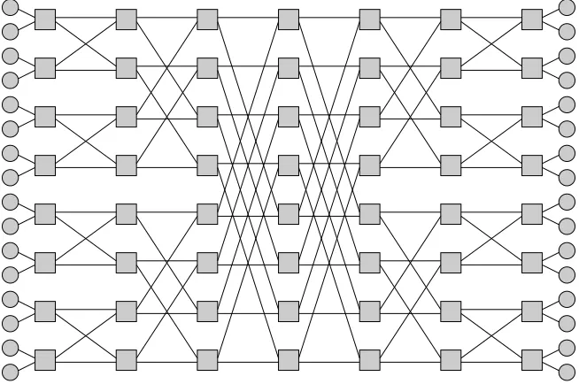
Figures 1.2-1.5 show examples of some standard network topologies which were consid-ered. The 2D mesh is shown in Fig. 1.2(a). The 2D torus of Fig. 1.2(b) is similar, but has wrap-around links such that the nodes along a dimension form a ring instead of a line, all nodes would then have a constant degree of four. The 3D torus and mesh networks are sim-ple extensions, analogous to the extension from a square to a cube. Fig. 1.3 shows a standard butterfly interconnection network. As shown data will only flow in one horizontal direction, but the assumption is that the corresponding functional units on the left and right represent the same physical processing element. The clos (Fig. 1.4) and flattened butterfly (Fig. 1.5) net-works are extensions of the regular butterfly network. The flattened butterfly network often groups switches even further than that in Fig. 1.5(a) and with processing elements into a single node, to reduce hop count and increase switch radix. As seen in Fig. 1.5(b), it is implemented as a concentrated mesh network where nodes along a dimension are fully connected.
with reasonable cost. The flattened butterfly especially has a low network diameter, and since it is based on a clos network, has path diversity unlike traditional butterfly networks [13].
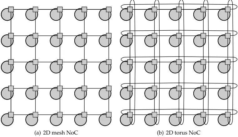
(a) 2D mesh NoC (b) 2D torus NoC
Figure 1.2: 5× 5 2D mesh and torus (5-ary 2-cube) NoC’s. The circles represent processing elements, and the squares represent routers. Routers which overlap processing elements make up a single NoC node.
Figure 1.3: A 2-ary 4-fly butterfly NoC. The circles represent processing elements, and the squares represent routers. Each router and each processing element is its own NoC node.
(a) Flattened butterfly (b) Flattened butterfly layout
routing latency in the network. Additionally, it is important to consider the scalability, cost, I/O bandwidth, routing path diversity, and hierarchy of the network.
The algorithm by which messages are routed through the network is clearly dependent upon the topology chosen. There is often a tradeoff between the quality of the routing al-gorithm and the complexity of the hardware, meaning that for a given topology the more intelligent the routing algorithm, typically the larger and more complex the control hardware. We must pay particular attention to this tradeoff, as the routing hardware is replicated in each node. Routing algorithms can be minimal or non-minimal, specifying whether routes from source to destination always use the minimum possible number of hops. Minimal routes are shorter and have require less complex hardware, but allowing non-minmal routes increases path diversity and decreases network congestion. An algorithm can be adaptive, where rout-ing decisions are made based on network congestion and other information about network links passed from neighboring nodes, or alternatively are deterministic. There is, however, a difference between deterministic routing and oblivious routing; deterministic routers can still make decisions based on contention for output ports. Oblivious routing does not consider that state of the network traffic or other messages in the network in any way when making routing decisions, it is typically implemented as a look up table. In this work we will use a different deterministic, non-oblivious routing algorithm for each topology.
examine all messages are only one flit long, so while buffering is used for performance and deadlock-avoidance, store-and-forward versus wormhole routing is not an issue.
Most of the remaining decisions are part of establishing the flow control of the network. Primarily, flow control is the mechanism by which network resources (mainly buffer space and link access) are allocated to messages in transit. It also dictates how nodes communicate to send messages. In addition to data being passed between nodes there is some type of control signaling to ensure that messages are not dropped due to contention. It is often implemented as an acknowledge/not acknowledge (ack/nak) or a credit based protocol. The network ar-chitectures investigated in this work use an on/off system, which is similar to the credit based protocol. Other flow control design decisions include the amount and type of flit buffering the network will use, if it is beneficial to use multiple parallel links between nodes, and whether the network will be circuit switched or packet switched. Circuit switched networks reserve all resources needed for communication and establish a channel before sending data, and when all of the data is sent the connection is torn down. There is often a significant delay in estab-lishing the channel, but once established, data transfer is usually very fast. Conversely, packet switched networks send flits as resources allow, cutting back on the initial setup time. Circuit switched networks are normally used when there is a lot of data to be exchanged between two nodes at one time, making it worthwhile to set up the dedicated channel. With our single flit messages, we need only consider packet switched networks.
1.3
Contribution
1.3.1 NoC Architectural Evaluation
is a methodology by which system architects can effectively evaluate the tradeoffs associated with NoC design, so that they have the necessary information to make design decisions. This contribution is made in three stages. In Chapter 4 we will describe the design of our general router, and how it is broken down into a set of reusable parameterized router components. We will continue to discuss a characterization methodology for these components, so that we can quickly and easily estimate the power, performance, and area overhead for the wide range of NoC’s that can be created from the components. We provide this finished characterization so that it may be used for architectural evaluation independent from the remainder of our sim-ulation framework. Secondly, Chapter 5 will serve to show how we use the NoC component characterization as part of a high level cycle accurate NoC simulator. We describe the architec-ture of this simulator to show how we predict the power, performance, and area of a complete application specific NoC system. Finally, in Chapter 6 we build upon our high level NoC sim-ulator and characterization to study how different architectural parameters affect the power and performance of NoC based low density parity check decoders.
ran-dom traffic. The cycle-accurate C++ model keeps track of cycle counts and transaction data for each module, and has access to the power, performance, and area models for each high level module, built from the simulation based characterization. Therefore, it can produce fast and accurate power, operating speed, throughput, and area data for any set of design parameters that we wish to explore.
Also considered in the evaluation will be the global interconnect. This includes all top level wires needed to interconnect the circuit modules that make up a node, as well as the NoC links. The rigorous power analysis is performed by a simulation framework based on EDA tools. As part of evaluating an architecture, the NoC simulator uses the generated area models to create a floorplan for the entire system, specific to the configuration of interest. The floorplan is written to an OpenAccess database, from where we can import it into industry-standard design tools, and within which we estimate the length of every wire needed. Using technology parameters and our transaction data, we can determine how these wires affect the critical path and find their power consumption. While the models we have prepared, the simulator written, and the design study performed all are based on NoC optimization, this simulation philosophy can be applied to any digital design. However, the modularity, component reusability, and large number of required architectural decisions make on-chip networks an excellent candidate for such an approach.
required by this simulator necessitates significant effort to adapt it to new network protocols and applications. It is modular and completely customizable for a user with intimate knowl-edge of its details, however it is not a fully automated NoC synthesis tool. We feel that a simulation platform of this specificity is absolutely required to optimize an application spe-cific NoC. We will now introduce the application chosen for our NoC study demonstrating our interconnection network simulator.
1.3.2 LDPC Decoding
As mentioned, the study of an NoC is only useful if realistic traffic patterns are used. As a practical example to produce such traffic patterns, we have chosen low density parity check (LDPC) decoding to be the application of our interconnection networks [14]. LDPC decoding is a very powerful linear error correcting coding (ECC) algorithm that has been around since roughly 1962. The iterative probabilistic decoding algorithm has a minimum coding distance that grows linearly with code length, and errors up to the minimum distance can be corrected with nearly linear complexity. It has had limited utility for a long time because it required far too much processing power for the real-time applications for which ECC algorithms are typically needed. However, it has been shown that irregular LDPC codes with large code block lengths have excellent coding performance, coming closer to the Shannon Limit than any other ECC algorithm [15]. Recently as digital chips have become more powerful, LDPC decoding has been used in some major communication standards, perhaps most notably the DVB-S2 standard for digital video broadcasts. It is also used in the Worldwide Interoperability for Microwave Access (WiMAX) standard for wireless data transfers and as part of the 802.3an 10 GbE ethernet specification.
reached. The throughput performance of LDPC hardware is very dependent upon the qual-ity of the fabric over which these messages are passed. Within an iteration of the decoding algorithm, the evaluation of one bit does not depend upon any others, allowing a high degree of computational parallelism. Performing LDPC decoding over an interconnection network has several advantages. First, many common LDPC implementations pass messages through memory accesses. In this case the memory bandwidth is an extreme bottleneck, so we in-stead spread this communication out over an entire network. Next, using an NoC allows us to carefully tune the level of parallelism without redesigning hardware. The algorithm lends itself to nearly any level of parallelism, so choosing a network topology that is incrementally expandable gives great flexibility in trading off die area and power for decoding throughput. For a given code block size and code rate, the decoding performance is heavily dependent on the parity check matrix. The parity check matrix defines the message passing pattern of the processing units. Due to the computational nature of LDPC decoding, many hardware implementations contain optimizations that increase hardware performance but place restric-tions on the parity check matrix. When an implementation uses an interconnection network for message passing, any processing element has the ability to communicate with any other. Therefore, except for overall system memory constraints, there are no restrictions on the parity check matrix to be used. The connectivity information of the parity check matrix is loaded into the chip during the configuration stage and remains that way until reset, making the LDPC NoC completely reconfigurable with respect to code block size, code rate, and parity check matrix.
Chapter 2
Related Work
This chapter first summarizes the previous contributions of other researchers in the areas of NoC design in Sec. 2.1. We will examine how other researchers have addressed the complexity of NoC design, discussing the most significant contributions in network router circuit archi-tectures, power estimation, topology selection, and automated NoC synthesis over the past few years. Designing on-chip interconnection networks is a very challenging task, there are many architectural decisions to make which control a sensitive power/performance/area bal-ance. How to manipulate this balance through NoC design decisions is typically not intuitive. There are well known methods to predict digital hardware performance and interconnection network characteristics, however it is difficult to accurately and quickly estimate power for large NoC systems in a way efficient enough for architectural exploration. No previous NoC design methodology addresses these difficulties as well as our methodology, introduced in Sec. 1.3.1.
unlike most being designed today. The chapter concludes with Table 2.1, a summary of the state-of-the-art LDPC decoder hardware.
2.1
Network-on-Chip Design
A good summary of the present status of NoC design is provided by Agarwal [16]. The authors address NoC topologies, router architecture, routing protocol, switching techniques, flow con-trol, virtual channels, buffering, error correction, transmission lines, network interface, quality of service, arbitration, applications, design methodologies, serial/parallel links, interconnect optimization, and other topics. In the next sections we will address a subset of these areas.
2.1.1 Network Simulators
It is common for NoC designers to use existing network simulation platforms for design ex-ploration. One of the most common network simulators is the ns-2 from Berkeley. It is an open-source discrete event network simulator, used most commonly to model both wired and wireless, local and wide area networks. It incorporates many standard protocols and network topologies, while also being compatible with customized protocols. Due to the high level sim-ilarities between NoC’s and networks, it has been used by NoC design researchers recently, even though it was intended for use with off-chip networks. By nature, it is best suited to helping make the highest level design decisions.
in-creasing number of transistors that can fit on a digital IC, integration of multiple synchronous clock regions, and global communication with low power and area overhead. The simple net-work is scalable and can be implemented with simple multiplexor based switch circuitry, even when including input buffer queues for improved congestion handling.
The most interesting contribution of this work was the investigation into buffer size within switches. They were able to show that message delay increases with buffer size, but that mes-sage delay is more sensitive to network load than to buffer size. They are able to determine the buffer size that results in nearly a zero probability of message drop, and the level of network loading that makes it impossible to avoid dropping messages. While the work of [17] does not allow for variation of topology, functional unit modeling, uses only random traffic patterns, and does not discuss circuit characterization, it is able to perform this analysis using the ns-2 generic network simulator.
net-work simulators may assist in the high level design decisions and be able to analyze general network characteristics, but will force a design team to change frameworks to perform any circuit based tradeoff analysis.
The open-source Noxim network-on-chip simulator written in SystemC has also emerged as a tool useful in NoC design. Unlike the ns-2 it is specifically tailored to on-chip networks, but the simulator does not allow the designer much flexibility, for example, you cannot choose your own topology. You can, however, vary the table based routing algorithm, buffer size, and input traffic characteristics. It can be used to determine network delay characteristics and energy consumption, however documentation is not available so we cannot be sure how the power analysis is performed or of its accuracy. Researchers including Flich and Duato [19] have used Noxim in publications evaluating a distributed routing algorithm. Network sim-ulators can be helpful when making architectural decisions based on network characteristics, but normally do not have knowledge of the circuits implementing the network and therefore are not very effective in predicting power. We will now discuss network analysis methods more specific to on-chip interconnection networks
2.1.2 Router Architecture
network performance where multiple virtual channels are multiplexed over a single physical link. In [20], Dally explains that the standard virtual channel router, as shown in Fig. 2.1, has an input unit with buffers for each port, routing hardware to implement the routing function, a virtual channel allocator, a switch allocator, a crossbar, and an output unit for each port.
1996 2003 2010 1991 1 10 100 1000
10 100 1000 10000
Aspect Ratio
Op
timal Radix (k)
Figure 2.
Relationship between optimal latency radix and
router aspect ratio. The labeled points show the approximate
aspect ratio for a given year’s technology
0 50 100 150 200 250 300
0 50 100 150 200 250 radix
latency (nsec)
2003 technology 2010 technology
0 1 2 3 4 5 6 7 8
0 50 100 150 200 250
radix
cost ( # of 1000 channels)
2003 technology 2010 technology
(a)
(b)
Figure 3.
(a) Latency and (b) cost of the network as the radix
is increased for two different technologies.
nate the overall latency and latency increases. As bandwidth,
and hence aspect ratio, is increased, the radix that gives
min-imum latency also increases. For 2003 technology (aspect
ratio = 554) the optimum radix is 40 while for 2010
technol-ogy (aspect ratio = 2978) the optimum radix is 127.
Increasing the radix of the routers in the network
monotonically reduces the overall cost of a network.
Net-work cost is largely due to router pins and connectors and
hence is roughly proportional to total router bandwidth: the
number of channels times their bandwidth. For a fixed
net-work bisection bandwidth, this cost is proportional to hop
count. Since increasing radix reduces hop count, higher
radix networks have lower cost as shown in Figure 3(b).
4Power dissipated by a network also decreases with
increas-ing radix. Power is roughly proportional to the number of
router nodes in the network. As radix increases, hop count
decreases, and the number of router nodes decreases. The
power of an individual router node is largely independent of
4
2010 technology is shown to have higher cost than 2003 technology
because the number of nodes is much greater.
the radix as long as the total router bandwidth is held
con-stant. Router power is largely due to I/O circuits and switch
bandwidth. The arbitration logic, which becomes more
com-plex as radix increases, represents a negligible fraction of
total power [33].
3
Baseline Router Architecture
The next four sections incrementally explore the
micro-architectural space for a high-radix virtual-channel (VC)
router. We start this section with a baseline router design,
similar to that used for a low-radix router [24, 30]. We see
that this design scales poorly to high radix due to the
com-plexity of the allocators and the wiring needed to connect
them to the input and output ports. In Section 4, we
over-come these complexity issues by using distributed allocators
and by simplifying virtual channel allocation. This results in
a feasible router architecture, but poor performance due to
head-of-line blocking. In Section 5, we show how to
over-come the performance issues with this architecture by adding
buffering at the switch crosspoints. This buffering eliminates
head-of-line blocking by decoupling the input and output
al-location of the switch. However, with even a modest number
of virtual channels, the chip area required by these buffers
is prohibitive. We overcome this area problem, while
retain-ing good performance, by introducretain-ing a hierarchical switch
organization in Section 6.
Switch Allocator VC Allocator Output k Crossbar switch Router Routing computation Output 1 VC 1 VC 2 VCv VC 1 VC 2 VCv Input 1 Input k
Figure 4.
Baseline virtual channel router.
A block diagram of the baseline router architecture is
shown in Figure 4.
Arriving data is stored in the input
buffers. These input buffers are typically separated into
sev-eral parallel virtual channels that can be used to prevent
deadlock, implement priority classes, and increase
through-put by allowing blocked packets to be passed. The inthrough-put
Figure 2.1: Virtual channel router [21]
rout-ing and bidirectional network links. As we use mesh, torus, flattened butterfly and fully con-nected topologies, the parameterized routers used in this work are a combination of the ones described here, tailored to the small message size and bursty traffic of LDPC decoding.
2.1.3 Power Estimation
There are many ways to compute the power consumption of circuits and systems. Different ways require different levels of circuit and switching activity detail, trading off accuracy for computation time. The ORION power-performance simulator [24] is widely used for the anal-ysis of a broad range of interconnection networks, both on-chip and off-chip. ORION predicts the power of a router based on the power consumption of the FIFO buffers, crossbars, and arbiters, components that consume 90% of the circuit area of a typical router. It uses very de-tailed models for power predictions based on computingP= 12fclkαCVdd2for the internal nets of the module of interest. Device and wiring capacitance parameters are computed by ORION using Cacti [25], while device sizes can be input by the user or determined using CACTI and a set of scaling parameters. Net switching activity is based on network simulation and estima-tion techniques. Addiestima-tionally, ORION is hierarchical, so large macros can be modeled based on its sub-blocks. This comprehensive tool is used by many including the creators of SUN-MAP [26], to be discussed in Sec. 2.1.4. A portion of the proposed work is similar in nature to ORION, however arrives at power estimates using parameterized router modules and scripts that stitch together commercial EDA tools to build power models based on simulation. Many of the same effects are accounted for, however making the high level power models available to the system simulator allows power estimation without performing a detailed net by net power computation each time, thus making the calculations faster. Furthermore, the power models in our work are built upon technology data and simulation, not CACTI estimates.
Sim-ilar comparisons show Orion 2.0 to be more accurate, in the two studies the power predictions were off by 6.5% and 11% while the area estimates were off by about 25%. Among other im-provements, Orion 2.0 brings flip-flop and clock modeling, enabling the modeling of flip-flop based FIFO’s, link and clock power models, and an automatic flow for extracting technology parameters from Liberty, LEF, PTM, and ITRS files to make updates easily obtainable.
Ye, et al. take a different approach, modeling switch fabric power consumption using a combination of a custom platform and industry EDA tools [28]. They feel that there is no one method that adequately models power consumption for all three types of interconnection net-work router power sinks, internal node switches, internal buffers, and the links which connect the switches. The authors explain the way the energy consumed per bit is computed for each of these sinks. Node switch power consumption is different from the others, because the en-ergy required to process a single bit is dependent upon the state of the switch. As the payload varies, or as the number of switch ports that are in use changes, the energy per bit varies. Since it is not a simple linear relationship, the best way to characterize the energy consumption is to use pre-calculated lookup tables created with the Synopsys Power Compiler tool. Internal buffers are created using SRAM or DRAM memory, and data is typically accessed a word or a byte at a time. The energy consumed per bit is the sum of the average access energy (a read or write operation) and the refresh energy (for DRAM). The energy per bit consumed on a network link is calculated using the standard formula,Ewirebit = 12V2 Cwire+Cinput
, where
Cinputis the input capacitance of the next gate. The value ofCwireis dependent on wire length,
2.1.4 Network Topology Selection
The proposed NoC evaluation methodology allows for expansion to analyze additional topolo-gies and routing algorithms. However, much of the decision of which topolotopolo-gies to include in this analysis is based on the work of Dally. As will be discussed, our analysis will be limited to 2D and 3D mesh and torus networks, the flattened butterfly topologies, and fully connected NoC’s. The flattened butterfly topology as described by Kim, Balfour, and Dally [13], is an indirect high radix interconnection network. Recent technology scaling trends have made on-chip bandwidth plentiful, and studies have shown that it is more advantageous for inter-connection networks to use this increased bandwidth to create additional narrow channels as opposed to creating fewer wide channels. The shift toward additional narrow channels leads us toward higher radix network topologies. The flattened butterfly topology when imple-mented on-chip becomes a concentrated mesh where groups of nodes along a dimension are fully connected. The work of [13] shows that the flattened butterfly is generally superior to the regular butterfly, clos, hypercube, and concentrated mesh topologies. They also discuss a number of potential optimizations and improvements on the topology and various methods to scale it to large networks. Three dimensional IC’s provide even larger on-chip bandwidth increases, further motivating high radix network investigation. We will continue to study the mesh and torus networks because of their simplicity and scalability, and because of other work that shows their advantages.
po-tential design they evaluate the latency, power consumption, and area, and choose one based on the highest priority constraint. Using the×pipes library and×pipesCompiler [29, 30], spe-cific SystemC code describing the network is generated. Area calculations based on the×pipes library include the crossbar, buffers, and control logic. Power analysis is performed using us-ing ORION [24], as described in Sec. 2.1.3. SUNMAP is very useful for topology selection, as it allows designers to evaluate several different topologies very quickly. It is not difficult to create additional NoC topology graphs so that a study can consider additional topologies. The authors use SUNMAP to choose topologies for two applications, giving an example of a case where the optimal network topology depends on the purpose of the network. It is shown that for their VOPD implementation a butterfly network is best, but for MPEG4 processing, a mesh topology is preferable. A combination of the methodologies of Murali and Benini, to be discussed in Sec. 2.1.5, will provide an NoC designer with a fair amount of insight as to how to create an optimal NoC for a specific application [26, 31].
Being an all-inclusive design tool, SUNMAP targets a different purpose from the proposed simulation platform. It is useful to automatically evaluate communication fabric topologies for SoC cores, however is subject to some important limitations. First, we are still limited by the
2.1.5 Automated NoC Design Tools
Perhaps the most interesting and relevant work has been that of Benini in automated NoC design. In [31], he presents the×pipes NoC Synthesis Flow which builds upon SUNMAP [26]. The flow makes use of the×pipes Lite interconnection networks macro library [29], combined with the compatible library compiler [30], the same library and compiler used in [26]. It is a nearly fully automated design methodology where a user specifies an NoC frequency range, link width, and the number of network switches, a value analogous to the concentration factor. The user also inputs traffic characteristics, sizes of the NoC cores, and network component area and power models are obtained. As the tool iterates through the user-set architectural parameter ranges, each potential network configuration is synthesized. Each design is then floorplanned, so link power consumption and operating frequency can be estimated, and it can be checked for timing violations. In the final phase register transfer level or SystemC code is generated for the network configuration that best meets the design objectives. The code is then synthesized, and a traditional back-end place and route design flow takes over to complete the NoC design.
A case study compares two implementations of an application specific NoC comprised of embedded processors, memories, and other components. One was hand-designed and opti-mized over the course of weeks, and the other was generated in a few hours using the×pipes NoC Synthesis Flow. The automated flow was set to minimize power consumption while tar-geting the same operating frequency of the hand-optimized design. A detailed analysis shows the hand optimized design to occupy 4.3% less area, but consume 33% more power while having the same operating frequency. Both implementations were to network identical hard-ware but had very different topologies, the automated design used roughly half the number of switches as the hand optimized design, thereby made up of higher radix switches. It resulted in an NoC with a 10% reduction in total execution time and 11% reduction in average packet latency.
when the time to market for a complex chip does not allow for proper design and charac-terization of NoC hardware. It is extremely useful when we are sure that a custom direct or indirect network topology is best for our application, though it does not allow for bounded hop networks such as the butterfly or clos. Also, such an automated design flow restricts the designer to the×pipes Lite library. The NoC is forced to use source routing dictated by routing tables to implement the routing algorithm, neither simple algorithms well suited for a standard topology nor more complex adaptive or dynamic algorithms are allowed. More complex designs that require support for virtual channel management or error detection can use the original×pipes library, while simpler ones that do not need such features can enjoy reduced pipeline depth and smaller areas by using the×pipes Lite library. However, this is a rather binary choice, and often we do not even need the complexity of the ×pipes Lite li-brary which implements packet retransmission and wormhole routing. Furthermore, though this approach allows for a description of traffic characteristics, we still cannot accurately pre-dict congestion without modeling the behavior of the processing elements. The×pipes NoC Synthesis Flow only accounts for module behavior in the final design stage, after all design decisions have been made. Lastly, without an explanation of module power characterization, we cannot know whether switch power models are solely based on radix and buffer size or if they also account for module switching activity and usage; power estimation, commonly re-garded as the primary goal in NoC design, is only as accurate as the module characterization on which it is based.
2.1.6 3DIC NoC Analysis
boundaries needed to route a single message in the network, as a function of the number of network nodes in each dimension. A simple model to compute arbiter delay is based on a technology parameter and the number of ports. Technology interconnect parameters and basic inverter characteristics are used to compute channel and crossbar delay, which when combined with arbiter delay estimation and expected hop counts, produce a theoretical model for the zero-load delay of a 3D NoC. The commonly used interconnect models to find chan-nel delay were adopted from [33], in [32] they were well modified for application to inter-tier interconnect. Power analysis is also theoretical; dynamic, short-circuit, and leakage powers are each considered separately. Considering only the horizontal and vertical interconnects, and crossbar power consumption, the authors arrive at an expression for the total minimum power consumed per bit for routing from source to destination, given a delay constraint, again in the zero-load situation.
Although only 2D and 3D mesh networks are considered, it is fortunate that Pavlidis and Friedman compare all four alternatives that result from considering 2D and 3D meshes in 2D and 3D technologies. The lack of a real application, traffic patterns, contention, simulated hardware, and additional interconnection network topologies leave plenty of room for inves-tigation with our proposed simulation platform. Though only the zero-load case is considered, it is very interesting and promising that for all cases the theoretical analysis showed the 3D NoC implemented on a 3DIC to be superior. Networks of between 16 and 2048 nodes are considered, and in each case the analysis shows the 3DIC-3D NoC to have the lowest latency and lower power consumption, while in all cases the 2DIC-2D NoC had the highest. Whether the 2DIC-3D NoC or the 3DIC-2D NoC is optimal varies, again all for the zero-load network traffic case.
throughput, latency, energy, and area. Traffic patterns from actual applications are considered through the use of a cycle-accurate network simulator. It is shown that both mesh and tree-based NoC’s benefit from implementation in a 3DIC technology. Mesh tree-based architectures were specifically tailored to a 3DIC implementation, and showed significant throughput, la-tency, and energy dissipation gains, with a small area overhead. Tree based 3DIC NoC’s have lower energy dissipation and area overhead, but similar throughput and latency to their 2D counterparts. Generally, the fat tree and stacked mesh seem to have the best performance.
2.2
LDPC Decoding
2.2.1 The LDPC Decoding Algorithm
The low density parity check algorithm is a product of the independent work of Gallager [14] and MacKay [35]. The brief description of the algorithm in this section is a convenient combi-nation of their notations and that of [36], for a deeper description of the algorithm one should consult the cited references. The LDPC belief propagation algorithm is an iterative message passing ECC algorithm in which messages regarding the probability of the value of a bit in a codeword are passed between two types of nodes, code nodes and check nodes.
There exists one code node for each bit in the codeword, to begin the algorithm each code node receives a single bit of the binary phase shift keying (BPSK) modulated codeword. After being transmitted over a noisy channel, the BPSK modulated value will be a value between -1 and 1. Each code node has knowledge of the variance of the noise introduced by the chan-nelN0
2
, and has the corrupted BPSK modulated value from the codeword to which it was assigned(rl). Thelth code node uses Eq. 2.1 to compute an initial probability, or initial belief that thelthbit of the codeword is a logic 1 p1l
. Similarly, according to Eq. 2.2, the initial belief that thelthbit of the codeword is a logic 0 p0l
is the compliment.
p1l = 1 1+exp
p0l =1−p1l (2.2)
Each code node participates in a number of parity checks, according to the parity check matrix. In a parity check matrix such as that in Fig. 2.2, the location of the 1’s in thelthcolumn specifies the parity checks in which thelthcode node is involved, or with which check nodes the lth code node exchanges messages. The set of check nodes with which code node l ex-changes messages is referred to asM(l). Similarly, the location of the 1’s in each row specifies with which code node each check node communicates. Check nodemis said to communicated with the set of code nodesL(m). Messages are iteratively exchanged between code nodes and check nodes according to the parity check matrix, until a certain maximum number of itera-tions is reached, or until the beliefs about all bits has reached a probability threshold, and the believed vector results in a valid codeword.
1 1 1 1 0 0 0 0 0 0 0 0 0 0 0 0 0 0 0 0 0 0 0 0 1 1 1 1 0 0 0 0 0 0 0 0 0 0 0 0 0 0 0 0 0 0 0 0 1 1 1 1 0 0 0 0 0 0 0 0 0 0 0 0 0 0 0 0 0 0 0 0 1 1 1 1 0 0 0 0 0 0 0 0 0 0 0 0 0 0 0 0 0 0 0 0 1 1 1 1 1 0 0 0 1 0 0 0 1 0 0 0 1 0 0 0 0 0 0 0 0 1 0 0 0 1 0 0 0 1 0 0 0 0 0 0 1 0 0 0 0 0 1 0 0 0 1 0 0 0 0 0 0 1 0 0 0 1 0 0 0 0 0 1 0 0 0 0 0 0 1 0 0 0 1 0 0 0 1 0 0 0 0 0 0 0 0 1 0 0 0 1 0 0 0 1 0 0 0 1 1 0 0 0 0 1 0 0 0 0 0 1 0 0 0 0 0 1 0 0 0 1 0 0 0 0 1 0 0 0 1 0 0 0 0 1 0 0 0 0 0 0 1 0 0 0 0 1 0 0 0 0 1 0 0 0 0 0 1 0 0 0 0 1 0 0 0 0 1 0 0 0 0 1 0 0 1 0 0 0 0 0 0 0 1 0 0 0 0 1 0 0 0 0 1 0 0 0 0 1
A parity check matrix can be more conveniently represented as a bipartite Tanner graph. In the Tanner graph of Fig. 2.3, the open circles(◦)represent the code nodes, and the closed circles (•)represent the check nodes of the corresponding parity check matrix, shown in Fig. 2.2. A message sent from code nodelto check nodemregarding belief that the bit is a 1 is denoted q1m,l, and a message regarding the belief that the bit is a 0 is denotedq0m,l. In the first iteration of the algorithm each code node sends its messages to the check nodes to which it is connected in the Tanner graph, we initializeq1m,l = p1l andq0m,l = p0l.
Figure 2.3: Tanner graph representation of the parity check matrix from Fig. 2.2
Once a check node receives messages from all of its code nodes, it can compute unique responses back to each of the code nodes from which it received a message. Eq. 2.3 shows that a message from check node mto code node l, denotedr1m,l or r0m,l, is calculated from the messages received from all of the code nodes with which it communicates, L(m), except for code nodel.
r( 0 1)
m,l =
1 2 ·
1
+
−
∏
l0∈L(m)\l
q0m,l0−q1m,l0
(2.3)
In iterations after initialization, the code node to check node message calculation depends upon both the initial beliefs, and the messages received from the check nodes. For the remain-der of the execution of the algorithm, the messages q0
q0m,l = p0l
∏
m0∈M(l)\m
r0m0,l (2.4)
q1m,l = p1l
∏
m0∈M(l)\m
r1m0,l (2.5)
Before sending to the check nodes, the messages q0m,l and q1m,l are normalized according to Eqs. 2.6 and 2.7.
q0m,l = q 0 m,l
q0m,l+q1m,l (2.6)
q1m,l = q 1 m,l q0m,l+q1
m,l
(2.7)
Also after receiving all of its messages from the check nodes, each code node must update its current beliefs that its bit is a logic 0 q0
l
and that its bit is a logic 1 q1 l
. This is computed using all of a code node’s incoming messages as shown in Eqs. 2.8 and 2.9, then the beliefs are normalized as in Eqs. 2.10 and 2.11.
q0l = p0l
∏
m∈M(l)
r0m,l (2.8)
q1l = p1l
∏
m∈M(l)
r1m,l (2.9)
q0l = q 0 l q0l +q1
l
(2.10)
q1l = q 1 l
q0l +q1l (2.11)
calculation within an iteration depends upon any other. Therefore given enough computing resources, within an iteration all code node calculations can be carried out in parallel, and all check node calculations can be carried out in parallel.
To simplify the hardware needed to perform LDPC decoding, instead of working with probabilities, we can perform the computation in the log-likelihood domain. Using this ap-proach, we can turn the multiplication in each node calculation into addition, thus using smaller, faster, and less power hungry circuits. Also, for simplicity, we can work with only likelihoods that the bit of interest is a logic 1. In this case, we compute the code node initial beliefs as in Eq. 2.12, whereRis the code rate, andSNRrefers to the signal to noise ratio of the channel.
pl =2·
q
2·R·10SNR10 ·rl (2.12)
δrm,l =
∑
l0∈L(m)\l
ln e
|qm,l0|+1 e|qm,l0| −1
!!
(2.13)
rm,l =ln
eδrm,l+1 eδrm,l−1
·
∏
l0∈L(m)\l
(sgn(qm,l0)) (2.14)
qm,l = pl+
∑
m0∈M(l)\m
rm0,l (2.15)
ql = pl+
∑
m∈M(l)
rm,l (2.16)
The check node computation is as described by Eqs. 2.13 and 2.14. The lne|x|+1
e|x|−1
function is normally implemented via a lookup table without significant loss of accuracy, and the
There are other optimizations to simplify the computation of the code nodes and check nodes in the LDPC decoding algorithm, but the aspect of the algorithm interesting to this work is the nature of the message passing between the two types of nodes. The parity check matrix is typically sparse, limiting the number of edges in the Tanner graph, but there is still a great deal of communication required. In Sec. 2.2.2 several LDPC implementations will be discussed, which handle the inter-node communication in a variety of ways. In this work we propose implementing an LDPC decoder on an interconnection network. A variable number of computational units can perform both the check node and code node operations; theoretical LDPC code nodes and check nodes are mapped onto a number of physical computational units. The computational units are connected via an on-chip interconnection network, over which all messages will be passed. This allows for an extremely flexible and scalable LDPC implementation, with performance and power consumption dependent upon the quality of NoC design. The remainder of this work will investigate methods to search for an optimal NoC design for a specific application, such as LDPC decoding.
2.2.2 LDPC Decoder Implementations
As discussed in Sec. 1.3.2, there has recently been a good deal of interest in LDPC decoder design. Over the past few years many LDPC architectures have been published, mostly ones which are heavily optimized for a specific set of codes. This makes sense because given con-straints on the parity check matrix, communication between check nodes and code nodes can be greatly simplified.
area also limits parallel implementations to small code block sizes, and using all dedicated wires is very difficult with limited on-chip routing resources. The LDPC decoder of [37] is lim-ited to a specific 1,024 bit block, rate12 code, a block size significantly smaller than that needed to realize the true ECC performance of the LDPC algorithm. Recently, Zhou and Shi [38] have built upon the work of Blanksby and Howland, by creating a similar 1,024 bit, rate 12 fully par-allel LDPC decoder in a 3D technology. Though the logic cell placement density on the chip was only 50% due to routing congestion, the 3DIC implementation has a 63% reduction in total wire length over an equivalent 2D design, equating to a 60% reduction in power dissipation.
Alternatively, there are the partially parallel LDPC decoder implementations such as that of Urard, et al. [39]. Their chip uses a constant 360 parallel physical processing LDPC mod-ules to implement all of the LDPC codes compliant with the DVB-S2 specification. In the case of partially parallel LDPC implementations, each physical processing element performs the task of one or more code and/or check nodes. While the architecture of [39] is optimized and only compatible with the DVB-S2 codes, it is a more versatile architecture as it handles both of the codeword block sizes of the DVB-S2 specification, 16,200 and 64,800 bits. Mes-sage passing does not use dedicated wires, but is achieved via memory accesses. This allows a shared message passing fabric, and depending upon the specific configuration of which memories and processing units are interconnected, allows a certain degree of code flexibil-ity. However, in such implementations the memory bandwidth becomes the performance limiting constraint. The authors of [40] also describe a highly optimized LDPC implementa-tion that passes messages via shift registers, but their design also can only decode DVB-S2 compliant codes. Karkooti, et al. discuss in [41] an LDPC decoder chip compatible with the IEEE 802.11n standard. In a 130µm technology the decoder of [41] occupies 3.7 mm2, and can achieve throughputs ranging from 250-700 Mb/s while dissipating 502 mW of dynamic power.
![Figure 1.1: Delay for metal 1 and global wiring versus feature size [2].](https://thumb-us.123doks.com/thumbv2/123dok_us/1600125.1197649/15.612.103.532.72.375/figure-delay-metal-global-wiring-versus-feature-size.webp)