ABSTRACT
XU, JIAN. AC Coupled Interconnect for Inter-chip Communications. (Under the direction of Prof. Paul D. Franzon.)
The scaling of integrated circuit (IC) technology demands high-speed, high-density
and low-powerinput/output (I/O) for inter-chip communications. As an alternative scheme
for conductive interconnects, AC coupled interconnect (ACCI) was proposed previously to
meet these increasing I/O requirements. ACCI includes AC coupling elements into a signal
channel; it has contactless physical structure and band-pass channel characteristic. ACCI can
be classified into two categories: capacitively coupled interconnect (CCI) that includes series
capacitors, and inductively coupled interconnect (LCI) that includes spiral transformers. This
dissertation addressed research progresses on both CCI and LCI for multi-Gb/s inter-chip
communications.
System analysis and transceiver circuit design for CCI chip-to-chip communications
are presented. In a demonstration for CCI on multi-chip module (MCM), two flip chips
communicated pseudo random bit sequence (PRBS) signals at 2.5Gb/s data rate through
chip-substrate interface capacitors. In a demonstration for CCI on print circuit board (PCB),
two bare chips communicated data at 2.0Gb/s through on-chip capacitors. Potential
applications of high-permittivity materials and embedded capacitors for CCI interfaces were
also investigated.
This work explored LCI vertical connections in three-dimensional (3D) ICs. A novel
current-mode LCI transceiver circuit is presented. In measurements, two test chips stacked
and communicated data at 2.8Gb/s through an inter-chip transformer. Misalignment and
AC connections through LCI interfaces and DC connections at chip edges, is proposed. A
novel 3D-ICs structure, which combines LCI vertical connections and 3D vertical vias, is
also presented. In measurements, eight LCI vertical channels operated simultaneously at
1.25Gb/s data rate.
This work also explored LCI interfaces in package-board sockets and board-board
connectors. Analysis and electromagnetic (E-M) modeling for interface transformers are
addressed. MCM test vehicles were designed to demonstrate chip-to-chip communications
over LCI. Simulations indicated a LCI transceiver system could communicate data at 2.0Gb/s
through a pair of coupled spiral inductors.
In conclusion, ACCI can provide feasible high-density high-speed and low-power I/O
AC COUPLED INTERCONNECT
FOR INTER-CHIP COMMUNICATIONS
by
JIAN XU
A dissertation submitted to the Graduate Faculty of North Carolina State University
in partial fulfillment of the requirements for the Degree of
Doctor of Philosophy
ELECTRICAL ENGINEERING
Raleigh 2006
DEDICATION
BIOGRAPHY
ACKNOWLEDGEMENTS
I sincerely thank my Ph.D advisor, Prof. Paul Franzon, for giving me this long-term academic training. Paul trusted and encouraged me to explore new research topics and alterative approaches. He has brought me many opportunities for chip tape-out and made advanced EDA tools and test equipments available. In spite of his busy schedule, Paul always keeps tracking my research progresses and direction. He also supported me to do internships and gave advice on my career plan.
I would like to thank my co-advisor, Dr. John Wilson, for providing me detailed technical guidance. John was deeply involved in all my research sessions: from idea discussions to chip designs, from data measurements to paper writing. I want to thank Dr. Rhett Davis, Dr. Jon-Paul Maria and Dr. Kevin Gard for their suggestions on this research work. I also want to thank Dr. Edward Grant and Dr. Angus Kingon for their advice on my previous “micro-robotics” research project.
I want to thank Stephen Mick, Lei Luo, Liang Zhang, Karthik Chandrasekar, Steve Lipa, Evan Erickson, David Winick, Zhiping Feng, Hao Hua, Julie Oh, Yongjin Choi and Bruce Su from the ECE department at NCSU for valuable discussions on this work. I appreciate Taeyun Kim from the MSE department at NCSU, Richard LaBennett and Salvatore Bonafede of RTI, for their collaborative work.
TABLE OF CONTENTS
CHAPTER 1. INTRODUCTION...1
1.1. MOTIVATIONS AND OBJECTIVES...1
1.1.1. Research Motivations ...1
1.1.2. Research Objectives ...2
1.2. ORIGINAL CONTRIBUTIONS...2
1.2.1. Capacitively Coupled Interconnect ...2
1.2.2. Inductively Coupled Interconnect...3
1.3. DISSERTATION OVERVIEW...4
1.4. PUBLICATIONS LIST...5
1.4.1. Journal Papers ...5
1.4.2. Conference Papers ...5
1.4.3. Presentations ...7
CHAPTER 2. LITERATURE REVIEW...9
2.1. OVERVIEW...9
2.2. ICPACKAGING HIERARCHY...9
2.3. ACCOUPLED INTERCONNECT...11
2.4. CHIP-TO-CHIP COMMUNICATIONS...14
2.4.1. Conductive Chip-to-Chip Communications...14
2.4.2. Non-contacting Chip-to-Chip Communications ...15
2.5. INTER-CHIP COMMUNICATIONS IN THREE-DIMENSIONAL ICS...16
2.5.1. Three-dimensional ICs Overview ...16
2.5.2. Conductive Vertical Interconnections ...17
2.5.3. Capacitively Coupled Vertical Signaling...18
2.5.4. Inductively Coupled Vertical Signaling...20
CHAPTER 3. CAPACITIVELY COUPLED INTERCONNECT (CCI) IN CHIP-TO-CHIP
COMMUNICATIONS ...23
3.1. OVERVIEW...23
3.2. ANALYSIS FOR CAPACITIVE COUPLING CHANNELS...23
3.2.1. Frequency Domain Analysis...23
3.2.2. Time Domain Analysis...25
3.3. CHARACTERIZATION FOR CAPACITIVE COUPLING INTERFACES ON MCM ...29
3.3.1. Coupling Capacitance of Metal Plate Pair with Air Gap...29
3.3.2. Coupling Capacitance of Metal Plate Pair with Epoxy Under-fill...31
3.3.3. Coupling Capacitance of Metal Plate Pair with High-k Under-fill...32
3.3.4. Parasitic Capacitance of Metal Plate Pair...35
3.4. CAPACITIVE COUPLING TRANSCEIVER CIRCUIT DESIGN...36
3.4.1. Single-ended Transceiver Circuit ...36
3.4.2. Differential Transceiver Circuit ...40
3.5. DEMONSTRATION OF CAPACITIVELY COUPLED INTERCONNECT ON MCM ...42
3.5.1. Overview...42
3.5.2. Test Chip and MCM Design ...44
3.5.3. Test Structures ...46
3.5.4. Measurement Results ...47
3.6. DEMONSTRATION OF CAPACITIVELY COUPLED INTERCONNECT ON PCB...48
3.6.1. Overview...48
3.6.2. Test Chip and PCB Design ...49
3.6.3. Measurement Results ...51
CHAPTER 4. INDUCTIVELY COUPLED INTERCONNECT (LCI) FOR VERTICAL CONNECTIONS IN 3D-ICS ...55
4.1. OVERVIEW...55
4.3. INDUCTIVELY COUPLED INTERCONNECT IN A TWO-CHIP STACK...58
4.3.1. Overview...58
4.3.2. Transceiver Circuit Design...58
4.3.3. Experiment Scheme...60
4.3.4. Experiment Results ...63
4.3.5. Misalignment Tolerance ...64
4.3.6. Crosstalk...66
4.3.7. Summary ...67
4.4. LCI IN A TWO-CHIP STACK WITH EDGE DCCONNECTIONS...68
4.4.1. Physical Structure...68
4.4.2. Transceiver Test Chip...70
4.4.3. Transceiver Circuit Design...71
4.5. LCI IN MULTI-CHIP THREE-DIMENSIONAL ICS...72
4.5.1. Physical Structure...72
4.5.2. Transceiver Test Chip...73
4.5.3. Transceiver Circuit Design...74
4.5.4. Transceiver Measurement Results ...75
4.5.5. Transformer Measurement Results...77
CHAPTER 5. INDUCTIVELY COUPLED INTERCONNECT (LCI) IN CHIP-TO-CHIP COMMUNICATIONS ...80
5.1. OVERVIEW...80
5.2. LCIPOTENTIAL APPLICATIONS IN CHIP-TO-CHIP COMMUNICATIONS...80
5.2.1. LCI at Package-Board Socket Interfaces...81
5.2.2. LCI at Board-Board Connector Interfaces ...82
5.2.3. LCI at 3D-ICs Cube-to-Cube Interfaces...83
5.3. CHANNEL CHARACTERIZATION FOR LCICHIP-TO-CHIP COMMUNICATIONS...84
5.3.1. LCI Transceiver System for Chip-to-Chip Communications ...84
5.3.3. Inductor and Transformer Modeling ...88
5.3.4. Transmission Line Modeling ...92
5.3.5. Frequency Response for a LCI Transceiver System ...94
5.4. PULSE SIGNALING IN LCICHIP-TO-CHIP COMMUNICATIONS...95
5.4.1. LCI Transceiver System...95
5.4.2. LCI Transmitter Circuit...95
5.4.3. LCI Coupling Interface...96
5.4.4. LCI Receiver Circuit...97
5.4.5. LCI Transceiver Test Chip...99
5.4.6. Simulation Results ...100
CHAPTER 6. CONCLUSIONS AND FUTURE WORK ...102
6.1. CONCLUSIONS...102
6.1.1. Capacitively Coupled Interconnect (CCI) ...102
6.1.2. Inductively Coupled Interconnect (LCI) ...103
6.1.3. Comparisons for CCI and LCI ...104
6.2. FUTURE WORK...106
6.2.1. CCI with Embedded Capacitors ...106
6.2.2. CCI at Package-to-Board Socket Interfaces...110
6.2.3. LCI Application on Chip-to-Chip Communications ...111
BIBLIOGRAPHY 115 APPENDIX A. FULLY-DEPLETED SOI TECHNOLOGY...122
APPENDIX B. THREE-DIMENSIONAL ICS TECHNOLOGY...123
APPENDIX C. MULTI-CHIP MODULE WITH BURIED BUMPS ...124
APPENDIX D. TRANSMISSION LINE MODELING...126
APPENDIX G. SCHEMATICS OF TRANSCEIVER CIRCUIT ...135
G.1. TSMC-0.35mM TEST CHIP FOR LCI IN 3D-ICS...135
G.2. TSMC-0.25mM TEST CHIP FOR LCI IN CHIP-TO-CHIP COMMUNICATIONS...136
LIST OF FIGURES
Figure 2.1. Overview of packaging hierarchy ... 10
Figure 2.2. Concept of AC coupled interconnect ... 11
Figure 2.3. A physical structure of ACCI on MCM ... 13
Figure 2.4. Integrating 2-D ICs to 3-D ICs... 16
Figure 2.5. Conductive vertical interconnections ... 18
Figure 2.6. An interface for capacitively coupled vertical signal transmission... 19
Figure 2.7. Cross-section of a proximity communication structure [25]... 20
Figure 2.8. Wireless superconnect (WSC) based on inductive inter-chip signaling ... 21
Figure 3.1. A simplified capacitive coupling channel ... 24
Figure 3.2. Frequency responses for various capacitive coupling channels ... 24
Figure 3.3. A simplified model for a capacitive coupling transmitter ... 26
Figure 3.4. Step responses for a capacitive coupling transmitter ... 27
Figure 3.5. A simplified model for a capacitive coupling receiver ... 27
Figure 3.6. Step responses for capacitive coupling channels... 29
Figure 3.7. Cross-section of a capacitive coupling interface with air gap... 30
Figure 3.8. Requirements of plate size for various air gaps... 30
Figure 3.9. Cross-section of a capacitive coupling interface with epoxy under-fill ... 32
Figure 3.10. Requirements of plate size for various epoxy filling thickness... 32
Figure 3.11. Cross-section of a capacitive coupling interface with high-k under-fill ... 33
Figure 3.12. Requirements of plate size for various high-k filling thickness ... 34
Figure 3.14. Parasitic capacitances for various coupling plate size... 36
Figure 3.15. Schematics of single-ended transceiver circuit for CCI... 37
Figure 3.16. Simulated eye-diagrams of signals over a CCI channel... 39
Figure 3.17. Schematics of differential transceiver circuit for CCI... 41
Figure 3.18. Schematic for CCI transceiver system on MCM... 43
Figure 3.19. Physical structures of CCI on MCM ... 43
Figure 3.20. Layout and micrographic of a TSMC-0.35mm test chip for CCI ... 44
Figure 3.21. Picture of a MCM under test (1.0”x0.5”) ... 45
Figure 3.22. Cross-section view for chip-substrate interfaces in a MCM ... 45
Figure 3.23. A test structure of a CCI transceiver system on MCM ... 46
Figure 3.24. A demonstration system for CCI on MCM with probes setting-up ... 46
Figure 3.25. Measured output waveform in CCI on MCM for 2.5Gb/s arbitrary data... 47
Figure 3.26. Measured eye-diagram in CCI on MCM for 2.5Gb/s PRBS... 48
Figure 3.27. Schematic of a CCI transceiver system on PCB ... 49
Figure 3.28. Layout and micrograph of a 0.18mm fully-depleted SOI test chip for CCI ... 50
Figure 3.29. A test vehicle to demonstrate CCI on PCB ... 50
Figure 3.30. A test structure of a CCI transceiver system on PCB... 51
Figure 3.31. Measured 3.0GHz clock waveform at RX output in CCI on PCB... 52
Figure 3.32. Measured 2.0Gb/s pattern waveform at RX output in CCI on PCB ... 52
Figure 3.33. Measured eye-diagram at RX output in CCI on PCB for 2.0Gb/s PRBS ... 53
Figure 4.1. Concept of inductively coupled interconnect (LCI) in 3D-ICs. ... 56
Figure 4.2. Dependence of coupling coefficient on separation distance ... 57
Figure 4.4. A transceiver circuit for LCI in 3D-ICs ... 59
Figure 4.5. Simulation results of a transceiver for LCI in 3D-ICs ... 60
Figure 4.6. Microphotograph of test chip for LCI in 3D-ICs (3.2x3.2mm2) ... 61
Figure 4.7. A demonstration system of LCI in a two-chip stack ... 62
Figure 4.8. Test structure for emulating 3D-ICs assembly... 62
Figure 4.9. Measurement results for 90mm thick LCI test chip in 3D-ICs. ... 63
Figure 4.10. Coupling coefficient sensitivity to horizontal offset ... 65
Figure 4.11. Shmoo plot for measured misalignment tolerances at 2.0Gb/s data rate ... 66
Figure 4.12. Test structure for measuring the crosstalk between neighboring inductors. ... 66
Figure 4.13. Measured isolation between two neighboring inductors ... 67
Figure 4.14. A combination of LCI interfaces and wire-bonding DC connections... 68
Figure 4.15. A combination of LCI interfaces and edge DC connections... 69
Figure 4.16. Layout and micrographic of a 0.18mm fully-depleted SOI test chip for LCI... 70
Figure 4.17. An asynchronous LCI transceiver circuit in 3D-ICs ... 71
Figure 4.18. Simulated eye-diagram at RX output for LCI with edge DC connections... 72
Figure 4.19. Combinations for ACCI interfaces and 3D vias... 73
Figure 4.20. Layout and micrographic of a 3D-ICs test chip for ACCI ... 74
Figure 4.21. An synchronized LCI transceiver circuit... 75
Figure 4.22. Test structure for LCI in multi-tier 3D-ICs ... 76
Figure 4.23. Eye-diagram at RX output for a synchronized LCI transceiver ... 76
Figure 5.1. Scheme for LCI at package-board socket interfaces ... 81
Figure 5.2. Scheme for LCI at board-board connector interfaces... 83
Figure 5.4. A transceiver system for LCI chip-to-chip communications ... 84
Figure 5.5. A “T” model for transformer analysis ... 85
Figure 5.6. Frequency responses for various coupling coefficient ... 86
Figure 5.7. Frequency responses for various self-inductances ... 87
Figure 5.8. Frequency responses for various DC resistances ... 87
Figure 5.9. Micrographic of a spiral inductor on a MCM substrate ... 88
Figure 5.10. An interface transformer in a 3D E-M field solver ... 89
Figure 5.11. An equivalent circuit for an interface transformer ... 90
Figure 5.12. Frequency response and input impedance of an interface transformer ... 91
Figure 5.13. Work flows for inductor/transformer design and modeling ... 92
Figure 5.14. A cross-section of two coupled micro-strip lines ... 93
Figure 5.15. Frequency response for a LCI signaling channel ... 94
Figure 5.16. A transmitter circuit in LCI chip-to-chip communications ... 96
Figure 5.17. Current waveform in a coupling transformer ... 97
Figure 5.18. A receiver circuit in LCI chip-to-chip communications... 98
Figure 5.19. Layout and micrographic of a TSMC-0.25mm test chip for LCI ... 99
Figure 5.20. A test structure for LCI in a two-MCM stack ... 100
Figure 5.21. Eye-diagram at RX output in a LCI transceiver system... 101
Figure 6.1. Capacitance of embedded capacitor on an ultra-thin PCB... 107
Figure 6.2. Schematic of CCI with an embedded capacitor ... 107
Figure 6.3. Pulse waveforms for various embedded capacitors... 108
Figure 6.4. CCI with an embedded capacitor and a passive equalizer ... 109
Figure 6.6. CCI application on package-board socket interface... 110
Figure 6.7. LCI application on chip-to-chip communications with two transformers... 111
Figure 6.8. A cascaded “T” model for a LCI system with two transformers ... 112
Figure 6.9. Frequency responses for a LCI system with two transformers ... 113
Figure 6.10. Eye-diagrams in a LCI system with two transformers ... 114
Figure A.1. Cross-section of a N-channel SOI transistor [43]... 122
Figure B.1. Cross-section of a 3D-ICs in FD-SOI technology [44] ... 124
Figure C.1. Cross-section of a MCM substrate for buried bumps ... 125
Figure C.2. Micrographic for a CCI interface in MCM... 125
Figure D.1. 3D view of a 50ohm micro-strip line on FR4 board... 126
Figure D.2. Frequency responses for a 10cm micro-strip line... 127
Figure E.1. Layout for an on-chip spiral inductor ... 128
Figure E.2. A “p” model for a spiral inductor ... 129
Figure E.3. 3D view of a transformer in Q3D field solver ... 130
Figure E.4. An equivalent circuit for a spiral transformer... 130
Figure E.5. Frequency response (S21) of a spiral transformer... 131
Figure F.1. Waveform of 2.5Gb/s NRZ and RZ signals... 132
Figure F.2. Spectrum of 2.5Gb/s NRZ and RZ signals... 133
Figure F.3. Waveform and spectrum of 2.5GHz bipolar RZ Pulses... 134
Figure G.1. TX circuit for LCI in 3D-ICs with TSMC-0.35mm technology ... 135
Figure G.2. RX circuit for LCI in 3D-ICs with TSMC-0.35mm technology... 135
Figure G.3. TX circuit in a LCI link with TSMC-0.25mm technology... 136
Figure G.5. TX circuit for LCI in 3D-ICs with FDSOI-0.18mm technology ... 137
LIST OF TABLES
Table 2.1. Signal channels for conductive chip-to-chip communications ... 14
Table 3.1. Bandwidth of capacitive coupling channel... 25
Table 3.2. Performance summary for CCI on MCM ... 48
Table 4.1. Performance summary for LCI in 3D-ICs ... 67
Table 4.2. Coupling pulses for various transformers... 78
Table 4.3. Coupling pulses for asymmetric transformer... 79
Table 5.1. W-element model for a pair of coupled transmission lines ... 93
Table 5.2. Summary for LCI test chip with TSMC-0.25mm technology... 101
LIST OF ABBREVIATIONS
3D-ICs, 3-D ICs Three-dimensional Integrated Circuits
ACCI AC Coupled Interconnect
BER Bit Error Rate
CCI Capacitively Coupled Interconnect
E-M Electromagnetic
ESD Electrostatic discharge
FD-SOI Fully-depleted Silicon on Insulator Gb/s, Gbps Gigabit per Second
I/O Input Output
ISI Inter-Symbol-Interference
ITRS International Technology Roadmap of Semiconductor LCI Inductively Coupled Interconnect
MIM Metal-Insulator-Metal
MCM Multi-Chip Module
NRZ Non-Return-to-Zero
PCB Print Circuit Board
PRBS Pseudo-Random Bit Sequence
RX Receiver
RZ Return-to-Zero
SAFF Sense Amplifier Flip Flop
SSN Simultaneous Switching Noise T-Line Transmission Line
TX Transmitter / Driver
TRX Transceiver
UI Unit Interval
XMFR Transformer
Chapter 1.
Introduction
1.1.
Motivations and Objectives
1.1.1. Research Motivations
The scaling of integrated circuit (IC) technology demands high-speed, high-density and low-powerinput/output (I/O) to provide Terabit/sec aggregate bandwidth for inter-chip communications. The International Technology Roadmap for Semiconductors (ITRS) website [57] predicts that in year 2013 the maximum pin-count in a high-performance single chip package will be 4736 and the data speed of chip-to-board peripheral buses will be 18.625GHz. AC coupled interconnect (ACCI) scheme uses contactless signal channels and transmits information on the transition edges of digital signals. ACCI is an alternative for conventional conductive interconnects and provides a solution to meet increasing I/O requirements. There are two types of ACCI: capacitively coupled interconnect (CCI) where coupling elements are formed using metal plate pairs, and inductively coupled interconnect (LCI) where coupling elements are formed using spiral inductor pairs.
high data rates require fast edge rates. While the data rates and edge rates continue to scale up with IC technologies, ACCI channels will more easily support high speed signaling.
For high-density package technologies, e.g. controlled-collapse-chip connections (C4) [52] in flip-chip packages, mechanical stress and thermal issues are one of the major limitations to achieving higher I/O density. ACCI interface has a non-contacting physical structure. It has the potential to overcome some of the mechanical and thermal constraints in building high-density I/O interfaces.
1.1.2. Research Objectives
The purpose of this work is to develop high-speed, high-density, low-power, low-cost and robust ACCI transceiver systems for chip-to-chip communications as well as vertical signaling in three-dimensional (3D) ICs.
1.2.
Original Contributions
1.2.1. Capacitively Coupled Interconnect
A MCM assembly was built to demonstrate 2.5Gb/s capacitive coupling communications between two flip-chips, where transceiver test chips were fabricated in 0.35mm CMOS technology and coupling capacitors were formed at the interface between the
flipped chips and the MCM.
A test vehicle on a PCB was built to demonstrate 2.0Gb/s capacitive coupling communications between two surface-mounted bare chips, where transceiver test chips were
fabricated in 0.18mm fully-depleted silicon-on-insulator (SOI) technology and coupling capacitors were on-chip metal-insulator-metal (MIM) capacitors.
This work explored the potential applications of high-permittivity under-fill materials and on-board embedded capacitors for CCI chip-to-chip communications, as well.
1.2.2. Inductively Coupled Interconnect
This dissertation describes theoretic analysis for LCI in both time domain and frequency domain. It also addresses characterizations for LCI channels and circuits design for LCI transceiver systems.
This dissertation presents a successful demonstration system for LCI vertical signaling in a three-dimensional (3D) IC. Two chips were stacked to demonstrate 2.8Gb/s inductively coupled vertical signaling in a 3D-ICs, where transceiver test chips were
fabricated in 0.35mm CMOS technology and coupled spiral inductors formed an inter-chip transformer.
presented an integrated 3D-ICs structure that combines LCI interfaces and 3D vertical via technologies. In demonstration, 8 LCI vertical channels operated simultaneously at 1.25Gb/s.
This work also explored LCI schemes for package-to-board socket and board-to-board connector interfaces to improve I/O pin density and create a reliable interface. Analysis and electromagnetic (E-M) modeling for interface transformers are addressed. MCM test vehicles were designed to demonstrate chip-to-chip communications over LCI.
1.3.
Dissertation Overview
1.4.
Publications List
1.4.1. Journal Papers
1. J. Xu, S. Mick, J. Wilson, L. Luo, K. Chandrasekar, E. Erickson, and P. Franzon, “AC coupled interconnect for dense 3-D ICs”, IEEE Trans. on Nucl. Sci., vol. 51, no. 5, Oct. 2004, pp. 2156-2160.
2. W. Davis, J. Wilson, S. Mick, J. Xu, H. Hua, C. Mineo, A. Sule, M. Steer, P. Franzon, “Demystifying 3D ICs: The pros and cons of going vertical”, IEEE Design & Test of Computers, vol. 22, no. 6, Nov. 2005, pp. 498-510.
3. L. Luo, J. Wilson, S. Mick, J. Xu, L. Zhang, and P. Franzon, “3Gb/s AC coupled chip-to-chip communication using a low swing pulse receiver”, IEEE J. of Solid State Circuits,
vol. 41, no. 1, Jan. 2006, pp. 287-296.
4. L. Zhang, J. Wilson, R. Bashirullah, L. Luo, J. Xu, P. Franzon, “Voltage-mode driver pre-emphasis technique for on-chip global buses”, IEEE Trans. on VLSI, (accepted) 5. J. Wilson, S. Mick, J. Xu, L. Luo, S. Bonafede, A. Huffman, R. LaBennett, P. Franzon,
“Fully integrated AC coupled interconnect using buried bumps”, IEEE Trans. on Advanced Packaging, (accepted)
1.4.2. Conference Papers
2. J. Xu, S. Mick, J. Wilson, L. Luo, K. Chandrasekar, E. Erickson, and P. Franzon, “AC coupled interconnect for dense 3-D ICs”, IEEE Nucl. Sci. Symp., Oct. 2003, pp. 125-129. 3. J. Xu, J. Wilson, E. Erickson and P. Franzon, “Pulse signaling in inductively coupled
sockets and connectors”, Semiconductor Research Corp. Student Symposium, Oct. 2006, paper 13.2
4. L. Luo, J. Wilson, S. Mick, J. Xu, L. Zhang, and P. Franzon, “A 3Gb/s AC coupled chip-to-chip communication with a low swing pulse receiver”, IEEE Int’l Solid-State Circuits Conf., Feb. 2005, paper 28.7, pp. 522-523.
5. L. Luo, J. Wilson, J. Xu, S. Mick and P. Franzon, “Signal integrity and robustness of ACCI packaged systems”, IEEE Topic Meeting on Electrical Performance of Electronic Packaging, Oct. 2005, pp. 11-14.
6. L. Luo, J. Wilson, S. Mick, J. Xu, L. Zhang, E. Erickson and P. Franzon, “A 36Gb/s ACCI multi-channel bus using a fully differential pulse receiver,” IEEE Custom Integrated Circuits Conf. (CICC), Sept. 2006, paper 26.3.
7. L. Zhang, J. Wilson, R. Bashirullah, L. Luo, J. Xu, P. Franzon, “Driver pre-emphasis techniques for on-chip global buses”, Int’l Symp. on Low Power Electronics and Design,
Aug. 2005, paper 7.2, pp. 186-191.
8. L. Zhang, J. Wilson, R. Bashirullah, L. Luo, J. Xu and P. Franzon, “A 32Gb/s on-chip bus with driver pre-emphasis signaling,” IEEE Custom Integrated Circuits Conf. (CICC),
Sept. 2006.
10.J. Wilson, P. Franzon, L. Luo, J. Xu, S. Mick, B. Chan and H. Lin, “AC coupled interconnect using buried bumps for laminated organic packages,” Electronic Components and Technology Conf., May 2006, paper 1.7.
11.J. Wilson, S. Mick, J. Xu, L. Luo, E. Erickson, and P. Franzon,, “Consideration for transmission line design on MCMs using AC coupled interconnect with buried solder bumps,” 10thIEEE Workshop on Signal Propagation on Interconnects, May 2006.
12.K. Chandrasekar, J. Wilson, E. Erickson, Z. Feng, J. Xu, S. Mick and P. Franzon, “Fine pitch inductively coupled connectors for multi-Gbps pulse signaling,” IEEE Topic Meeting on Electrical Performance of Electronic Packaging, Oct. 2006, paper 2.3.
13.K. Chandrasekar, J. Wilson, E. Erickson, Z. Feng, J. Xu, S. Mick and P. Franzon “Signal integrity analysis for inductively coupled connectors and sockets”, DesignCon 2007, paper 10-TA2 (accepted).
14.P. Franzon, A. Kingon, S. Mick, J. Wilson, L. Luo, K. Chandrasakhar, J. Xu, S. Bonafede, A. Huffman, C. Statler, R. LaBennett, “High Frequency, High Density Interconnect Using AC Coupling”, MRS Symp. Proc., vol. 783, B6.1
15.F. Libsch, R. Budd, P. Chiniwalla, P. Hobbs, M. Mastro, J. Sanford and J. Xu, “MCM LGA package with optical I/O passively aligned to dual layer polymer waveguides in PCB,” Electronic Components and Technology Conf., May 2006, paper 37.11.
1.4.3. Presentations
2. J. Xu, J. Wilson and P. Franzon, “Development of AC coupled interconnects for multi-gigabit/sec inter-chip communications,” 1st Annual NC State Graduate Student Research Symposium (Poster), Raleigh, NC, Mar. 2006
3. J. Xu, J. Wilson, and P. Franzon, “Development of multi-Gb/s AC coupled interconnects”,
IMAPS Carolina Scientific Symp, RTP, NC, Mar. 2006
4. J. Xu, J. Wilson, and P. Franzon, “A power delivery scheme for inductively coupled 3D-ICs,” IMAPS Carolina Scientific Symp (Poster), RTP, NC, Mar. 2006
5. J. Xu, J. Wilson, S. Mick and P. Franzon, “Development of multi-Gb/s AC coupled interconnects,” Semiconductor Research Corp. Contract Review (Poster), Palo Alto, CA, Aug. 2005.
6. J. Xu, J. Wilson and P. Franzon, “Development of AC coupled interconnects for multi-Gb/s inter-chip communication”, ECE Department Graduate Student Association Seminar, Raleigh, NC, Aug. 2005
7. J. Xu, J. Wilson and P. Franzon, “Development of multi-Gb/s AC coupled interconnects,”
IBM T.J. Watson Research Center Seminar, Yorktown Heights, NY, Aug. 2005.
Chapter 2.
Literature Review
2.1.
Overview
This chapter introduces the concept of AC coupled interconnect (ACCI), which includes capacitively coupled interconnect (CCI) and inductively coupled interconnect (LCI). It also summarizes the up-to-date publications on ACCI and similar technologies in chip-to-chip communications and vertical signaling in three-dimensional ICs.
2.2.
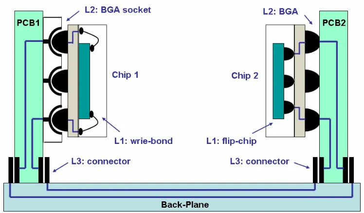
IC Packaging Hierarchy
where multiple chips are stacked on a base chip and encapsulated into a package. The interconnections in 3D-ICs include chip-to-chip vertical connections and the base chip to package connections.
In the second level (L2) packaging, a ceramic or organic package such as a pin-grid array (PGA) or ball-grid array (BGA) is mounted onto a printed circuit board (PCB). The interconnections in L2 packaging are at package-to-board interfaces. A special type of L2
packaging is a package-board adapter or socket that introduces more flexibility for manufacture/assembly. In the third level (L3) packaging, daughter cards are mounted onto a motherboard or backplane. The interconnections in L3 packaging are at board-to-board connector interfaces.
2.3.
AC Coupled Interconnect
AC coupled interconnect (ACCI) inserts AC coupling elements such as series capacitors and spiral transformers for inter-chip connections at L1~L3 packaging levels. It has a non-contacting structure and is an alternative scheme for conventional conductive interconnections to achieve multi-Gb/s communication data rate between ICs. Mick et al. (2002) presented the concept of ACCI [7], which includes two types: capacitively coupled interconnect (CCI) where the coupling elements are series capacitors formed by metal plate pairs, and inductively coupled interconnect (LCI) where the coupling elements are transformers formed by spiral inductor pairs.
(a) A capacitively coupled interconnect (CCI) transceiver system
(b) An inductively coupled interconnect (LCI) transceiver system Figure 2.2. Concept of AC coupled interconnect
Figure 2.2(a) shows a CCI chip-to-chip transceiver system. A voltage mode transmitter (TX) circuit drives the first series capacitor and converts non-return-to-zero (NRZ) digital signals into return-to-zero (RZ) pulses. These pulses propagate over a transmission
TX RX
line (T-line) and pass through the second series capacitor with some attenuation and distortion. A voltage mode receiver (RX) circuit senses the voltage pulses and restores them back to full-swing NRZ voltage signals. Although the transceiver system shown in Figure 2.2(a) has a single-ended structure, it can be a differential as well.
Figure 2.2(b) shows a LCI chip-to-chip transceiver system. A current mode TX circuit converts NRZ voltage signals into bipolar current swings. At the first transformer, the current swings excite the primary inductor and induce current pulses at the secondary inductor. These current pulses flow in the T-line and pass the second transformer with additional attenuation and distortion. A current mode RX circuit senses the current pulses and regenerates NRZ voltage signals.
Franzon et al. (2001) filed a patent on “inductively coupled electrical connectors” [53]. They also filed a patent on “Buried solder bumps for AC-coupled microelectronic interconnects” [54].
Mick et al. demonstrated a CCI transceiver system that transmitted 2GHz clock
signals. Test chips were fabricated in 0.25mm CMOS technology, and the coupling elements
were 0.8pF on-chip metal-insulator-metal (MIM) capacitors. In Mick’s Ph.D dissertation (2004) [1], he included detailed analysis of CCI and LCI interface models.
Figure 2.3. A physical structure of ACCI on MCM
Luo et al. (2005) presented capacitively coupled chip-to-chip communication using a low-swing pulse receiver [9][10][11]. They demonstrated two chips communicating across a 15cm PCB micro-strip line that connected 150fF on-chip coupling capacitors on each end through bonding wires. The novel low-swing differential pulse receiver was able to detect 60mV pulse signals and recover non-return-to-zero (NRZ) signals at the data rate of 3Gb/s. For 0.18μm CMOS test chips, each transceiver channel dissipates 15mW. They also discussed signal integrity and robustness issues in CCI packaged systems [11]. Luo presented timing circuits that include a delay-lock-loop (DLL) and clock-data-recovery (CDR) for CCI transceiver system in his Ph.D dissertation [2].
Chandrasekar et al. (2005) introduced inductively coupled board-to-board connectors [14][15]. They proposed to replace conventional connectors with coupled spiral inductors to increase I/O pin density, and reported simulation and measurement results for LCI interfaces
Trench DC Connection Interconnection Layer Trench DC Connection Chip 1 MCM Substrate Chip 2
Chandrasekar also described LCI channel modeling and system design tradeoffs in his Ph.D dissertation [3].
2.4.
Chip-to-Chip Communications
2.4.1. Conductive Chip-to-Chip Communications
Signal channels for conductive chip-to-chip communications on MCM, PCB and Backplane are described in Table 2.1.
Table 2.1. Signal channels for conductive chip-to-chip communications
MCM PCB Backplane
Package wire-bond or flip-chip Bare chip PGA, BGA or LGA Packaged chip PGA, BGA or LGA Packaged chip
T- lines Short lossy T-line on carrier (e.g. 1 inch)
T-line on board (e.g. 10 inch)
Two T-lines on cards, one long T-line on backplane (e.g. 25 inch) Parasitic
components Bonding wires or solder bumps Package leads, board vias, sockets Package leads, board vias, connectors
In a multi-chip module (MCM), multiple bare chips are mounted onto a common carrier or substrate via wire-bonding or flip-chip technologies. A signal channel for chip-to-chip communication in a MCM includes a short but lossy transmission line on the substrate and lumped parasitics for bonding wires or solder bumps.
trace stubs in packages, leads or balls of package pins, and via stubs on the board. A package-to-board adaptor or socket may also be included into the signal channels.
In a backplane system, multiple line cards are inserted into connectors or slots on a backplane. Signal channels for chip-to-chip communications in a backplane include traces and parasitic components on daughter cards, board-to-board connectors, long traces and via stubs on the backplane.
2.4.2. Non-contacting Chip-to-Chip Communications
Salzman et al. (1994) introduced capacitively coupled interconnect for chip-to-substrate interfaces in a multi-chip module [32][33]. Knight et al. filed two patents on capacitive coupling interfaces in 1994 [55] and in 1999 [56]. Hayden et al. (1994) introduced pulse-mode signaling for a capacitively coupled interconnect [37].
Gabara et al. (1996) described a technique of quantized feedback that eliminates the “zero wander” effect in capacitive coupling channel with an on-chip capacitor [35][36]. For
0.5mm CMOS test chips, this receiver circuit can detect PRBS data up to 800Mb/s and down to 2kHz.
Chang et al. (2001) introduced a concept of RF/wireless interconnect for inter-chip and intra-chip communications [18]. Unlike the conventional conductive interconnect, the novel RF/wireless interconnect is based on capacitive coupling onto a coplanar waveguide (CPW).
demonstrated 1.0Gb/s differential pulsed signaling over 10cm PCB lines. This system dissipates 1.92mW power per transmitter and 2.7mW power per receiver.
2.5.
Inter-chip Communications in Three-dimensional ICs
2.5.1. Three-dimensional ICs Overview
Three-dimensional (3D) ICs is a new chip/package architecture where multiple chips are stacked vertically. Banerjee et al. (2001) gave an overview on 3D-ICs technology [38]. It was shown that 3D-ICs can improve the availability of interconnect resources and significantly reduce interconnect delay. 3D-ICs can also facilitate integration of heterogeneous technologies in a single chip.
Figure 2.4 illustrates multiple planar chips, which includes a microprocessor chip, a memory chip, a digital signal processor (DSP) chip and a radio frequency (RF) module chip, integrated into a 3D-ICs stack.
Figure 2.4. Integrating 2-D ICs to 3-D ICs
2-D ICs (Planar) 3-D ICs (Stack)
uP Memory
DSP RF uP
However, 3D-ICs technology dramatically increases internal heat density [16]. The thermal management capability for 3D interconnects is a critical challenge predicted by the International Technology Roadmap for Semiconductors (ITRS) [57].
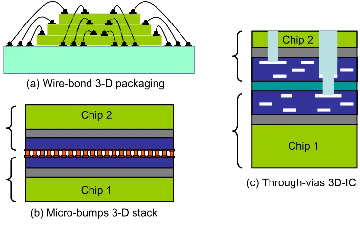
2.5.2. Conductive Vertical Interconnections
Al-Sarawi et al. (1998) gave a review of 3-D packaging technologies [45]. Brown (2004) gave an overview on system-in-package (SiP) technologies [41], he presented multiple thin chips that were stacked and connected through wire-bonding. Ezaki et al. (2004) reported a CPU-DRAM 3D chip stack [42], where the vertical connections between
chips consist of micro-bumps in 30mm diameter and 60mm pitch.
Black et al. (2004) demonstrated a 3-D implementation of an x86 microprocessor [39]. Two chips stacked face-to-face and connected through die-to-die vias. Compared to a 2-D planar implementation, the 3-D architecture could improve performance by 15% while decreasing power by 15%.
Suntharalingam et al. (2005) presented a mega-pixel image sensor fabricated in wafer level 3D-ICs technologies [40]. Two fully-depleted SOI dies and one photodiode die were thinned and stacked. Two bonded dies were connected by 3-D vias that used tungsten (W)
plugs with ~2mm square size and ~7.5mm depth.
(a) Wire-bond 3-D packaging
(b) Micro-bumps 3-D stack
(c) Through-vias 3D-IC Chip 2
Chip 1
Chip 2
Chip 1
Figure 2.5. Conductive vertical interconnections
2.5.3. Capacitively Coupled Vertical Signaling
Kuhn et al. (1995) proposed a signaling method for direct vertical transmission of digital signals between adjacent chip-layers in 3D-ICs by capacitive coupling [34]. The scheme of a capacitive coupling interface is shown in Figure 2.6, where the coupling pads occupied 20x20mm2 areaand separated vertically with a2.5mm dielectric layer. They chose
Figure 2.6. An interface for capacitively coupled vertical signal transmission
Kanda et al. (2003) presented a wireless superconnect (WSC) interface scheme for vertical signaling in 3D-ICs [26]. This scheme also utilizes capacitively coupled contactless mini-pads as chip-to-chip connection interfaces. The transmitter converts NRZ signals to return-to-half-Vdd signals and the receiver is based on a sense-amplifier flip-flop. They
demonstrated WSC using 0.35mm CMOS test chips, where each mini-pad was 20μm per side and the vertical distance between two mini-pads was 1~2μm, and each capacitive WSC I/O consumed 3mW power at 1.27Gb/s data rate.
Drost et al. (2003) proposed a proximity communication structure, shown in Figure 2.7, where chips overlap face-to-face and communicate via capacitive coupling interfaces on chip edges [23][24][25]. For 0.35mm CMOS test chips, they demonstrate 16 capacitive
coupling channels, placed in 50mm pitch and operated simultaneously. Each channel
Figure 2.7. Cross-section of a proximity communication structure [25] (Courtesy of Robert Drost, Sun Microsystems)
Gu et al. (2004) presented a RF-interconnect (RFI) technology based on capacitive
coupling and peak signal detection [19][20]. For 0.18mm CMOS test chips with 60fF
coupling capacitors, they demonstrated an amplitude-shift keying (ASK) transceiver system in 3D-ICs. The RF-interconnect transceiver communicated PRBS at 3Gb/s data rate, consumed 4mW power and maintained a bit error rate (BER) less than 10-10.
Fazzi et al. (2005) reported a synchronous 3D interconnection based on capacitive coupling [48]. They presented a capacitively coupled link consumed 0.128mW/pin power at 975Mb/s data rate, and the capacitive pad area was down to 8x8μm2.
2.5.4. Inductively Coupled Vertical Signaling
CMOS technology were stacked at a distance of 300mm. Transceiver circuits communicated NRZ signals at a data rate of up to 1.2Gb/s per pin, while the TX circuit consumed 43mW power and the RX circuit consumed 2.5mW power.
Figure 2.8. Wireless superconnect (WSC) based on inductive inter-chip signaling
Miura et al. (2005) reported inductively coupled wireless interface, which achieved an aggregated data rate of 195Gb/s by arranging 195 transceivers in 50µm pitch with total
power dissipation of 1.2W [28][31]. The chip thickness was thinned down to 10mm and the
communication distance was 15mm, including the glue thickness. The TX circuit used a
single-end structure and included a series compensation capacitor for reducing its DC power dissipation.
Miura et al. (2006) presented a 1024 transceiver array for inductive-coupling inter-chip communication in a two-inter-chip stack [29]. The inter-chip thickness was also thinned down to
10mm and the inductor pitch was 30mm. Each data channel operated at 1Gb/s and consumes
2.6.
Summary
Recently, ACCI attracts growing research interests in both academia and industry. CCI was proposed to apply on various areas such as vertical connections in 3D-ICs [26], edge-to-edge proximity communication [25], and multi-drop memory bus [22]. LCI was reported to apply on vertical connections in 3D-ICs [31].
In NC State University, Mick proposed a novel ACCI physical structure on MCM [1]; Luo reported differential transceiver systems for CCI on PCB, he also presented timing circuitry and signal integrity for CCI [2]; Chandrasekar described analysis and modeling for LCI interfaces [3].
Chapter 3.
Capacitively Coupled Interconnect (CCI) in
Chip-to-Chip Communications
3.1.
Overview
This chapter addresses the analysis for capacitive coupling channels and the characterizations for capacitive coupling interfaces. It describes pulse-mode signaling circuit design for capacitive coupling transceiver systems. It also presents capacitive coupling demonstration systems for chip-to-chip communications on MCM and PCB.
3.2.
Analysis for Capacitive Coupling Channels
3.2.1. Frequency Domain Analysis
By ignoring parasitic capacitances of coupling capacitors, a simplified capacitive coupling channel for chip-to-chip communications is shown in Figure 3.1. It includes a transmission line (T-line), a termination resistor (RT), a coupling capacitor (C1) at the TX
side and another coupling capacitor (C2) at the RX side.
A lossy T-line presents low-pass characteristic. For instance, a 10cm 50ohm
micro-strip line, which has 6.3mil trace width, 1oz (35mm) copper thickness and 4mil FR4 dielectric
Figure 3.1. A simplified capacitive coupling channel
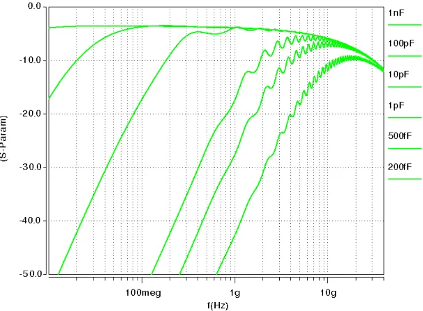
By adding a 50ohm termination resistor and two coupling capacitors which have capacitance variable in 200fF~1nF, AC analysis was performed and frequency responses (S21) for the capacitive coupling channel are shown in Figure 3.2. It can be observed that a
capacitive coupling channel presents band-pass characteristic, where the coupling capacitance (CC) defines the high-pass corner frequency (fhp) and the lossy T-line defines the
low-pass corner frequency (flp).
For various values of coupling capacitance, the corresponding bandwidths of the capacitive coupling channel are shown in Table 3.1. A channel with larger coupling capacitance, e.g. 1nF, has a lower fhp, e.g. 3.6MHz, and can passes most low-frequency
components of digital signals. Its band covers most of NRZ signal spectrum that is shown in Appendix F and it can support NRZ signaling with some coding scheme such as 8b/10b [4]. A channel with smaller coupling capacitance, e.g. 200fF, has a higher fhp, e.g. 7.83GHz, and
can only pass high-frequency components of digital signals. Its band covers RZ pulse signal spectrum that is also shown in Appendix F and it is suitable for pulse-mode signaling. If the coupling capacitance is in a range 5pF~100pF, the channel could support neither NRZ signaling nor RZ pulse signaling at multi-Gb/s data rate.
Table 3.1. Bandwidth of capacitive coupling channel
Coupling capacitance corner frequency High-pass corner frequency Low-pass Signaling method
1 nF 3.6 MHz 11.20 GHz NRZ
100 pF 38.4 MHz 11.20 GHz NRZ
10 pF 271.5 MHz 11.20 GHz None
1 pF 2.03 GHz 21.58 GHz RZ pulse
500 fF 3.67 GHz 29.86 GHz RZ pulse
200 fF 7.83 GHz 48.26 GHz RZ pulse
3.2.2. Time Domain Analysis
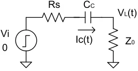
capacitance and the characteristic impendence of T-line, respectively. A 0àVi step function
is added as the source.
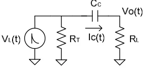
CC
Z0 Rs
Vi
VL(t) Ic(t)
0
Figure 3.3. A simplified model for a capacitive coupling transmitter
This circuitry has differential equations:
o c c c s
i Ri t v t i t Z
V = ( )+ ( )+ ( )
and dt t dv C t i c c c ) ( ) ( =
and an initial condition:
0 ) 0 ( Z R Vi i s c = +
There are solutions for the current in capacitor:
) ) ( exp( ) ( 0
0 s c
s c C Z R t Z R Vi t i + -+ =
and the voltage on T-line:
) ) ( exp( ) ( ) ( 0 0 0 c s s o c L C Z R t Z R Vi Z Z t i t V + -+ = =
This is the step response of the transmitter and has an decaying exponential waveform, where the time constant (Rs+Z0)Cc represents the decay time and the initial
value 0 0 Z R Vi Z s+
represents the maximum amplitude. For a capacitive coupling transmitter with
Figure 3.4. If Cc is smaller than 1pF, the decay time is short than 500ps, which means a
2Gb/s NRZ signal will be converted into RZ pulses. If Cc is larger than 100pF, the decay
time is much longer than 1ns, which means a 2Gb/s NRZ signal will pass the coupling capacitor and keep the NRZ shape.
Figure 3.4. Step responses for a capacitive coupling transmitter
A simplified model for capacitive coupling receiver is shown in Figure 3.5, where RT
and RL represent the termination resistance and the input impedance of receiver. Assuming
the T-line is an ideal transmission line without any attenuation, the source for this receiver model equals the voltage on T-line VL(t), which is given by the previous solutions.
This circuitry has differential equations:
L c c
L t v t i t R
V ( )= ( )+ ( )
and dt t dv C t i c c c ) ( ) ( =
and an initial condition:
L s c R Z R Vi Z i ) ( ) 0 ( 0 0 + =
There is a solution for the voltage at the receiver input:
:= ( )
Vo t Rl ic( )t = Rl
æ è çç çç ö ø ÷÷ ÷÷ -
Vi Zo e
æ è
çç-t(Rs(Rl + - - Zo Cc RlRs) Zo)ö÷÷ø
(Rs + Zo)(Rl - - Rs Zo)
Vi Zo
Rl (Rl - - Rs Zo) e
æ è
çç-Rl Cct öø÷÷
A capacitive coupling transceiver system includes two differentiation elements, it has a second-order transfer function and its step response is a combination of two exponential waveforms. For RS=50ohm, Z0=50ohm, CC=0.2pF, RT=50ohm, and RL=50~1000ohm, step
responses at receiver input are shown in Figure 3.6. If RL equals 50ohm, the voltage
waveform at the receiver input will have large overshoot, also referred to as a double pulse. If RL is larger, e.g. 500ohm, the overshoot will be much smaller. A high input impedance of
receiver RL increases the damping factor of the system transfer function and limits the
overshoot to avoid double pulses.
Actually, in circuit simulations for a capacitive coupling transceiver system, the overshoot or double pulse at the second coupling capacitor was not significant because the input impedance of receiver RL is typically much larger than 50ohm. It can also be explained
frequency (f1) is defined by 1/((RS+Z0)*CC), where RS is typically around 50ohm. For the
second coupling capacitor, its corner frequency (f2) is defined by 1/(RL*CC), where RL is
typically around 500ohm. As (RS+Z0) << RL, then f1 >> f2, the second coupling capacitor has
a lower high-pass corner frequency and a wider bandwidth than the first coupling capacitor. A pulse generated by the first coupling capacitor can pass the second coupling capacitor without creating a significant double pulse.
Figure 3.6. Step responses for capacitive coupling channels
3.3.
Characterization for Capacitive Coupling Interfaces on MCM
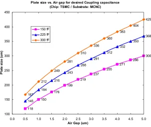
3.3.1. Coupling Capacitance of Metal Plate Pair with Air Gap
maintain an air gap between them. A process overview of MCM with buried solder bumps is described in Appendix C.
Figure 3.7. Cross-section of a capacitive coupling interface with air gap
Plate size vs. Air gap for desired Coupling capacitance (Chip: TSMC / Substrate: MCNC)
118 150 176 199 219 237 255 271 286 300 145 184 216 243 268 291 312 332 350 368 167 212 249 281 310 336 360 383 404 425 100 150 200 250 300 350 400 450
0.0 0.5 1.0 1.5 2.0 2.5 3.0 3.5 4.0 4.5 5.0
Air Gap (um)
P la te s iz e (u m) 150 fF 225 fF 300 fF
Figure 3.8. Requirements of plate size for various air gaps Solder Bump
Air Gap Passivation
For desired coupling capacitances such as 150fF, 225fF and 300fF, curves for the
requirement of plate size in various air gap (0.5mm~5mm) are shown in Figure 3.8. The
passivation layer on top of metal plates, e.g. 1.7mm dielectric with a 0.3mm equivalent air gap,
is preferably kept for isolation. For a given coupling capacitance, the minimum size of
coupling plates strongly depends on the air gap. For instance, at 2mm air gap, a 200x200mm2 coupling plate pair is required to achieve a desired 150fF coupling capacitance. Such large size for a metal plate limits the density of coupling elements.
In the MCM assembly process, to achieve a 1~2mm air gap is feasible by controlling the volume of solder bumps. However, it is very difficult to maintain such a small gap evenly and constantly, due to the process variation and thermal expansion.
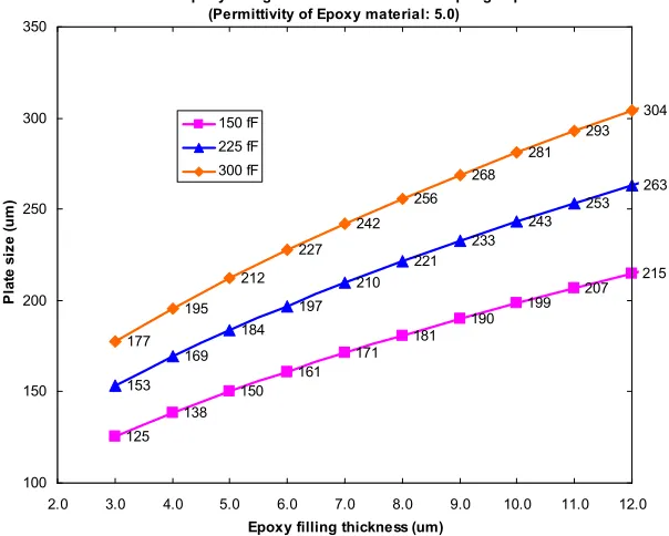
3.3.2. Coupling Capacitance of Metal Plate Pair with Epoxy Under-fill
Epoxy under-fill materials are commonly used in flip-chip processes to reduce the stress of solder bumps due to thermal mismatch between chips and substrate. A cross-section of capacitive coupling interface with epoxy under-fill on MCM is shown in Figure 3.9. Curves for the requirement of plate size in various epoxy under-fill thickness are shown in Figure 3.10.
Compared to the air gap capacitive coupling interfaces, plates sizes in the case of epoxy under-fill are reduced because the permittivity of epoxy material is higher than air gap, e.g. er=5. For 5mm epoxy filling, to achieve the desired 150fF coupling capacitance, coupling
Solder Bump Epoxy Under-fill Passivation layer Coupling Plates
Figure 3.9. Cross-section of a capacitive coupling interface with epoxy under-fill
Plate size vs. Epoxy filling thickness for desired Coupling capacitance (Permittivity of Epoxy material: 5.0)
125 138 150 161 171 181 190 199 207 215 153 169 184 197 210 221 233 243 253 263 177 195 212 227 242 256 268 281 293 304 100 150 200 250 300 350
2.0 3.0 4.0 5.0 6.0 7.0 8.0 9.0 10.0 11.0 12.0
Epoxy filling thickness (um)
P la te s iz e (u m) 150 fF 225 fF 300 fF
Figure 3.10. Requirements of plate size for various epoxy filling thickness
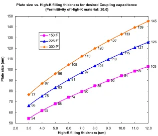
3.3.3. Coupling Capacitance of Metal Plate Pair with High-k Under-fill
desired capacitance for effective coupling due to the low permittivity of air gap (er=1). This
proximity requirement brings significant manufacturing challenges due to tolerance issues associated with such small dimensions.
Replacing the air gap with a high permittivity material can achieve higher capacitance density and thereby relax the proximity requirement between the chip and the substrate. Such a material can also provides stress relief by acting as an under-fill material and thus improves the overall reliability of capacitively coupled interconnect (CCI). Kim et al. developed a Barium Titanate (BaTiO3) and epoxy nano-composite, which has a permittivity up to 20 at multi-GHz and is a promising candidate for under-fill material in CCI [17].
A cross-section of capacitive coupling interface with high-k filling on MCM is shown in Figure 3.11. If the passivation layer on top of metal plates is removed, a high-k material is then used to fill the gap between coupling plate pairs. To reduce the un-wanted crosstalk between neighboring plates, the high-k under-fill layer needs be deposited with pattern rather than processed evenly.
Figure 3.11. Cross-section of a capacitive coupling interface with high-k under-fill Solder Bump
High-k Filling Passivation
For specified coupling capacitances, three curves of the requirement of plate size
versus various high-k filling thickness (er=20, 3~12mm) are shown in Figure 3.12. Compared
to the capacitive coupling interfaces with air gap, the required minimum size of coupling plates in the capacitive coupling interfaces with high-k filling is reduced significantly due to
the high capacitance density. For instance, at 3mm high-k underfill, the glass opening on top
of metal plates could be as small as 54x54mm2 to achieve the desired 150fF coupling
capacitance. Considering the glass-metal overlap, typically 10mm, coupling plates could be
64x64mm2. This would make a possible high-density capacitive coupling plates array with a
pitch less than 75mm.
Plate size vs. High-K filling thickness for desired Coupling capacitance (Permittivity of High-K material: 20.0)
54 62 68 74 80 85 90 94 99 103 66 75 83 91 97 104 110 115 121 126 77 87 96 105 113 120 127 133 139 145 50 60 70 80 90 100 110 120 130 140 150
2.0 3.0 4.0 5.0 6.0 7.0 8.0 9.0 10.0 11.0 12.0
High-K filling thickness (um)
P lat e siz e (u m) 150 fF 225 fF 300 fF
3.3.4. Parasitic Capacitance of Metal Plate Pair
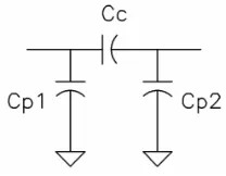
Beside the coupling capacitance, the parasitic capacitances of coupling plates need also be included in circuit simulations. Figure 3.13 shows a “pi” model of coupling plates, where Cc represents the coupling capacitance; Cp1 represents the parasitic capacitance of
plate on chip and Cp2 represents the parasitic capacitance of plate on substrate.
Figure 3.13. A “p” model for a coupling plate pair
For TSMC 0.18mm, 0.25mm and 0.35mm CMOS technologies, the unit area parasitic
capacitance of top layer metal is 3.0aF/mm2, 4.0aF/mm2 and 6.3aF/mm2, respectively. For the
MCNC (RTI) MCM process, the unit area parasitic capacitance is only 0.87aF/mm2. Ignoring
the fringe parasitic capacitances because of the relatively big plates, the relationships between parasitic capacitances and the size of coupling plates are shown inFigure 3.14.
As the coupling plates are placed on the top layer metal of chip, an older CMOS technology has less metal layers and thus a larger parasitic capacitance of coupling plates.
For a 200x200mm2 metal plate, the on-chip parasitic capacitance is 120fF, 160fF and 252fF
for 0.18mm, 0.25mm and 0.35mm technology, respectively. In the case of capacitive coupling
coupling capacitance. It will bypass a large amount of signal energy and reduce the effective signal strength especially at the input of RX circuit.
Parasitic Capacitance vs. Plate size for TSMC and MCNC processing
7.5 30 67.5 120 187.5 10 40 90 160 250 15.75 63 141.75 252 393.75 0 50 100 150 200 250 300 350 400 450
0 50 100 150 200 250
Plate size (um)
P aras it ic ca p ac ita n ce ( u m) TSMC-0.18um TSMC-0.25um TSMC-0.35um MCNC-BCB
Figure 3.14. Parasitic capacitances for various coupling plate size
3.4.
Capacitive Coupling Transceiver Circuit Design
3.4.1. Single-ended Transceiver Circuit
well as its parasitic capacitances. The first two inverters are sized to maintain a fast edge rates for the last inverter stage.
(a) Transceiver system
(b) Transmitter circuit
(c) Receiver circuit
Figure 3.15. Schematics of single-ended transceiver circuit for CCI
line will be degraded. Because the input impedance of RX circuit is much lager than the T-line characteristic impedance, the second series capacitor has a wider bandwidth than the first one. Those voltage pulses can pass the second series capacitor with some additional attenuation but little overshoot.
The function of a RX circuit is to sense the incident voltage pulses and restore them to full swing signals. A modified Kuhn receiver [34], shown in Figure 3.15c, was proposed to accomplish this function. Two feedback transistors, operating in the linear region, create a DC bias at half of the supply voltage (Vdd/2) for the first stage inverter and maintain that inverter amplifier to operate in the high gain region. Moreover, the feedback mechanism trades some inverter gain to expand the bandwidth of the inverter amplifier. The voltage pulses can be amplified with little distortion and it is very beneficial for jitter control. An inverter isolates the feedback from the rest of circuit and continues to amplify voltage pulses; a cross-coupled inverter pair forms a bi-stable latch to restore voltages pulses to NRZ signals; and the last two inverters are buffers to drive the output load.
For instance, a CCI channel includes two 150fF coupling capacitors and a 25cm
50ohm T-line, and transceiver circuits were designed in the TSMC-0.18mm CMOS technology. In simulation, source signals at the TX input are 5Gb/s PRBS data. Simulated eye-diagrams of signals along the CCI channel are shown in Figure 3.16.
(a) NRZ signals at TX output, (b) RZ pulses at line input, (c) Attenuated RZ pulses at T-line output, (d) Biased pulses at RX input
Figure 3.16. Simulated eye-diagrams of signals over a CCI channel
It can be observed that the pulses at the RX input have some overshoot, which is due to the differentiation property of the series capacitor. Because of the relatively high input impedance of the RX, e.g. 570ohm, the overshoot is damped to acceptable amplitude. The pulse width at the RX input is less than one UI. It will leave some margin for inter-symbol interference (ISI) at the RX circuit. The pulse shape is independent of the data pattern; it depends on the edge rate of NRZ data and is regulated by the CCI channel. The regulated narrow pulses are equalized signals to the RX circuit, so a CCI channel provides passive equalization and relieves the requirements of equalization in TX or RX circuits.
3.4.2. Differential Transceiver Circuit
A differential transceiver system for CCI is shown in Figure 3.17a, which includes a differential TX, a pair of coupled T-lines, two pairs of series capacitors, two terminators and a differential RX. A schematic of a differential TX, which includes two inverter chains operating complementary, is shown in Figure 3.17b.
(a) Differential transceiver (TRX) system
(b) Differential transmitter (TX) circuit
(c) Differential receiver (RX) circuit
In the sensing stage, feedback transistors build DC bias voltages for the inputs of RX and maintain the inverter amplifier to operate in a high gain region. In the latch stage, two cross-coupled transistors create a positive feedback mechanism that can accelerate transitions of the amplifier; two spanning transistors compensate the cross-coupled transistors and improve the stability of amplifier. The latch stage converters differential voltage pulses into large swing complementary signals, and the voltage buffers restore them to full swing complementary NRZ signals.
3.5.
Demonstration of Capacitively Coupled Interconnect on MCM
3.5.1. Overview
A demonstration system for CCI chip-to-chip communications on MCM was built and tested. Figure 3.18 shows a schematic for a CCI transceiver system on a MCM.
Transceiver test chips were fabricated in TSMC-0.35mm CMOS technology. A MCM silicon
substrate was fabricated by MCNC (RTI) with copper deposition and BCB spin-on technology. Test chips were flipped and assembled on the common substrate. Coupling capacitors were formed at the interfaces between the chips and the substrate; the coupling plate size was 200x200mm2 and the gap between two plates was approximately 1mm. A
5.6cm 50ohm micro-strip copper trace was placed in the BCB layers of the substrate to connect two series capacitors. Figure 3.19 depicts the physical structure for CCI in MCM, which include a 3-D view and a cross-section view.
Figure 3.18. Schematic for CCI transceiver system on MCM
(a) 3-D view for CCI on MCM
(b) Cross-section view for CCI on MCM Figure 3.19. Physical structures of CCI on MCM
TX RX
Coupling capacitor (200mm size, ~1mm gap)
5.6cm 50ohm micro-strip line
Driver chip Receiver chip
50ohm Termination
3.5.2. Test Chip and MCM Design
A CCI transceiver test chip (3.2x3.2mm2), shown in Figure 3.20, was fabricated in
0.35mm CMOS technologies. It includes single-ended circuits as well as differential circuit
with various coupling capacitances.
(a) Layout (b) Micrographic
Figure 3.20. Layout and micrographic of a TSMC-0.35mm test chip for CCI
Figure 3.22 depicts a cross-section view for chip-substrate interfaces. Solder bumps were buried into trenches in the substrate. They provide mechanical support as well as electrical DC connections to the flip-chip. Metal plate pair at the chip-substrate interfaces forms coupling capacitors.
Figure 3.21. Picture of a MCM under test (1.0”x0.5”)
3.5.3. Test Structures
A test structure of a CCI transceiver system for on MCM is shown in Figure 3.23. The input signals at the TX were delivered through a RF probe (GGB model 40A, 50ohm); the output signals at the RX were sensed through a high-impedance probe (GGB model 35, 50fF, 1.25Mohm). A demonstration system for CCI on MCM with input/output probes in place is shown in Figure 3.24.
Figure 3.23. A test structure of a CCI transceiver system on MCM
Figure 3.24. A demonstration system for CCI on MCM with probes setting-up
Pulse Pattern Generator Agilent 81134A
Power
Sampling Oscilloscope
Tek 11801A TX
Chip
BCB Substrate
3.5.4. Measurement Results
Two CCI channels operated simultaneously. One channel was fed by a 2.5Gb/s 32bit arbitrary pattern data, and the other channel was fed by a 2.5Gb/s PRBS data. The measured waveform at the RX output of the first channel is shown in Figure 3.25.
Figure 3.25. Measured output waveform in CCI on MCM for 2.5Gb/s arbitrary data
Figure 3.26. Measured eye-diagram in CCI on MCM for 2.5Gb/s PRBS
Table 3.2. Performance summary for CCI on MCM
Chip technology TSMC-0.35mm CMOS
MCM technology MCM-D with BCB
Supply voltage 3.3V
T-line length 5.6cm micro-strip line Coupling plate size 200x200 mm2
Data rate (PRBS) 2.5Gb/s per channel Power per channel TX: 10.3mW, RX: 15.0mW Bit error rate (BER) < 10-12
Jitter at RX out < 120ps peak-to-peak
3.6.
Demonstration of Capacitively Coupled Interconnect on PCB
3.6.1. Overview
were fabricated by MIT Lincoln lab in 0.18mm fully-depleted SOI technology, which is described in Appendix A; coupling capacitors were embedded in the test chips; bare chips were mounted on a PCB directly; a 17cm 50ohm micro-strip copper trace on the PCB connected two test chips via wire bonding.
For square-wave clock inputs, this transceiver system operates at a frequency up to 3.0GHz and consumes 9.90mW power. For arbitrary pattern data inputs, this transceiver system works at 2.0Gb/s data rate with 35% data activity and consumes 6.98mW power. For PRBS data inputs, this transceiver system consumes 7.35mW power at 2.0Gb/s data rate and maintains a jitter less than 80ps on the eye-diagram at RX output.
Figure 3.27. Schematic of a CCI transceiver system on PCB
3.6.2. Test Chip and PCB Design
A CCI transceiver test chip (3.0x3.0mm2), shown in Figure 3.28, was fabricated in
0.18mm fully-depleted SOI technology. It includes single-ended circuit as well as differential
circuit with various coupling capacitances. It also includes transceiver circuits for CCI
flip-TX RX
On-chip coupling
capacitor (206fF) Wire-bond
50ohm micro-strip line on PCB (17cm)
Transmitter chip