Doping concentration effect on performance of single QW
double-heterostructure InGaN/AlGaN light emitting diode
N. Syafira Abdul Halim1,*, M.Halim A. Wahid1, N. Azura M. Ahmad Hambali1, Shanise Rashid1, and Mukhzeer M.Shahimin21Semiconductor Photonics & Integrated Lightwave Systems (SPILS), School of Microelectronic Engineering, Universiti Malaysia Perlis, Pauh Putra Campus, 02600 Malaysia.
2Department of Electrical and Electronic Engineering, Faculty of Engineering, National Defence University of Malaysia (UPNM), Kem Sungai Besi, 57000 Kuala Lumpur.
Abstract. Light emitting diode (LED) employed a numerous applications such as displaying information, communication, sensing, illumination and lighting. In this paper, InGaN/AlGaN based on one quantum well (1QW) light emitting diode (LED) is modeled and studied numerically by using COMSOL Multiphysics 5.1 version. We have selected In0.06Ga0.94N as the active layer with thickness 50nm sandwiched between
0.15µm thick layers of p and n-type Al0.15Ga0.85N of cladding layers. We investigated an effect of doping
concentration on InGaN/AlGaN double heterostructure of light-emitting diode (LED). Thus, energy levels, carrier concentration, electron concentration and forward voltage (IV) are extracted from the simulation results. As the doping concentration is increasing, the performance of threshold voltage, Vth on one quantum well (1QW) is also increases from 2.8V to 3.1V.
1 Introduction
Wide band gap gallium nitride (GaN) based semiconductor device has become a great potential of electronic and semiconductor research community due to its extensive applications for optoelectronic devices in the blue and ultraviolet (UV) wavelength region. Gallium nitride (GaN) based LEDs have played a progressively imperative roles in countless promising reals, for instance, an exterior automobile lighting, traffic signals, backlighting sources for solid-state lighting and liquid-crytal displays (LCD) [1]. Thus, the wavelength range determines the LED applications for instance blue LED with 430nm-470nm is used for medical field while other range operates in different fields.
The improvement in these devices obtained by enhancing the device structure and quality is still on research progress which look forward to upgrading its efficiencies and performances. Efficiency droop effect [2], high forward voltage [3], current-crowding [4], low hole concentration in p-GaN [5] are such an obstacle that is still under research progress. Thus, several solutions have been introduced to overcome these problems. Besides, doping concentration also lead to a serious issues in GaN. It has been widely observed by many research communities that an electron mobility increases when the free electron concentration is decreased, and then decreases after a critical electron concentration is reached. The threshold voltage is typically in the low 1x1017cm-3 range and is dependent upon the threading
dislocation density. In this context, the improvement of increasing doping concentration in gallium nitride (GaN) LED structure has a great importance for better performances in GaN LED structure.
The modelling, design and to understand more into a complex nitrides device structure needs multiphysics tool [6]. Furthermore, during last few recent years, various method of numerical modelling and simulation of gallium nitride (GaN) based light-emitting diode (LED) have been published and develop [7-11]. Thus, for enhancing the device performance of GaN LED, typically the doping concentration plays an important roles to increase the great performance of light-emitting diode itself.
In this work, a study is performed to evaluate an effect of doping concentration on InGaN/AlGaN double heterostructure gallium nitride (GaN) LED. Fundamental relations such as the band diagram, carrier concentration, electron concentration, current-voltage characteristics (IV) are explored with different values of doping concentration.
2
LED device modeling
The device structure can be modeled using 1D line in Comsol. The lower AlGaN layer represents n-doped and the upper AlGaN layer denotes p-doped. Meanwhile, InGaN layer which is located in the centre between two AlGaN layers is undoped. This constructs a P-I-N diode structure with the central (intrinsic) undoped region, InGaN layer that emits light.
In this study, the boundary conditions referred to p and n metal contact boundary conditions are applied to InGaN/AlGaN double heterostructure LED. Moreover, the boundary conditions play an imperative roles as this feature is added to the bounds of device structure for applying voltages and currents to the device. Next, the boundary conditions are vital to toggle amid the continuous quasi-Fermi levels and thermionic emission heterojunction continuity models. In addition, optical transitions are applied in this model to calculate the value of spontaneous emission from LED. This is important as it will assist and make it straightforward to calculate the process such as atom or molecule transition from an excited energy state to a lower energy state and emits a quantum in the form of photon.
Besides, the number of doping concentration is applied for all domains of p and n-type AlGaN. The range of doping concentration is 1016 cm-3 to 1019 cm-3. This doping concentration range is a possible range for light-emitting diode devices to effectively operate in various applications.
Next, Auger recombination feature is added to the structure as it functionally to include a non-radiative recombination mechanism. Thus, this is the only possible non-radiative recombination mechanism, in fact a various technique may be present such as lattice or impurity scattering and phonon interactions. Besides, the purpose to display a proof model, Auger recombination is adequate to monitor the behaviour such as the efficiency is reduced as the current densities are increased. In addition, trap-asisted recombination feature is added to all domains in the LED structure.
In addition, mesh is applied onto the entire geometry of 1D of InGaN/AlGaN double heterostructure LED. The first distribution is developed for domain 1 and 3 only. Meanwhile, second distribution is built for domain 2 only. The mesh is important for a device structure as it can evaluate the transition area of electron and photon.
Afterwards, two types of studies which are preliminary study and bias voltage are evaluated and contemplated in this work for resolving the problems.
range from 0V to 3.3V. This feature extracts an energy level diagram for the device along with the carrier concentration distribution and the current-voltage characteristics (IV) relation.
Furthermore, the performance of single quantum well (1QW) InGaN/AlGaN double heterostructure LED is compared based on energy levels, carrier concentrations, current-voltage characteristics (IV) at different values of doping concentration in a range from 1x1016cm-3 to 1x1019 cm-3.
2
Simulation result and discussion
(a)
(c)
(d)
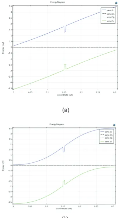
Fig. 2. Energy band diagram at 0V for doping concentration (a) 1x1016 cm-3(b) 1x1017 cm-3 (c) 1x1018 cm-3 (d) 1x1019 cm-3.
Fig. 2 depicts the energy band diagram at 0V for doping concentration of 1x1016 cm-3, 1x1017 cm-3, 1x1018 cm-3and 1x1019 cm-3. Based on the band diagram illustrated in Fig.2, the semi.Ec, semi.Ev, semi.Efn, semi.Efp are the designation for conduction band, valence band, quasi-Fermi level in region n and p respectively. It shows that the potential barrier is formed between the left side n-doped region and p-doped region. This occurs due to the potential well in both conduction and valence band are lower than the band gap of InGaN layer. Fig. 2(a) depicts a linear relation of energy diagram for both conduction and valence band at 0V for doping concentration of 1x1016 cm-3. Meanwhile, as
doping concentration increases from 1x1016 cm-3 to
1x1019 cm-3, the trend changes from linear to curvature
relation. This is because the number of holes and electron is increased due to the number of doping concentration which also increased in the recombination process. In addition at zero bias, the quasi-Fermi level is away from the band edges of InGaN layer for all modules.
(a)
(b)
(c)
(d)
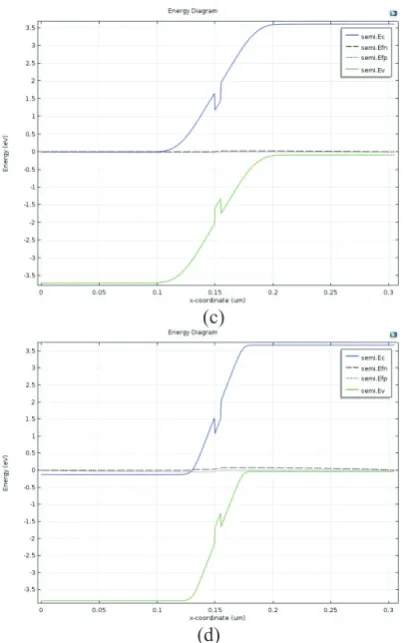
Fig. 3. Energy band diagram at 3.3V results for doping concentration (a) 1x1016 cm-3(b) 1x1017 cm-3 (c) 1x1018 cm-3 (d) 1x1019 cm-3.
form a junction.
(a)
(b)
(c)
(d)
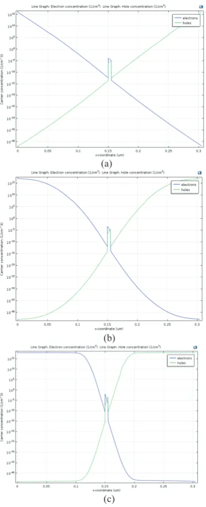
Fig. 4. Carrier concentration at zero bias (a) 1x1016 cm-3 , (b) 1x1017 cm-3 , (c) 1x1018 cm-3 , (d) 1x1019 cm-3
Fig. 4 demonstrates the carrier concentration involving both holes and electrons for different values of doping concentration in a range from 1x1016 cm-3 to 1x1019 cm-3. As illustrated in Fig. 4, as the number of doping concentration increases, the combination peak of holes and electron reaches approximately at the same level.
(a)
(c)
(d)
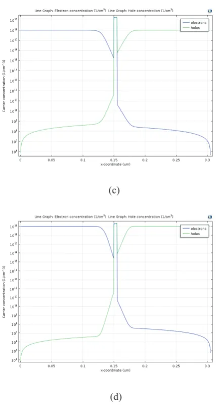
Fig. 5. Carrier concentration at 3.3V forward bias (a) 1x10¹⁶
cm-3, (b) 1x1017 cm-3 ,(c)1x1018 cm-3, (d) 1x1019 cm-3
As illustrated in Fig. 5, the carrier concentration versus device coordinate plot showed that the population of carriers in InGaN layer increased drastically with the increased bias of LED along with a different number of doping concentrations. This occurs as doping concentration is increased gradually from 1x1016 cm-3 to 1x1019 cm-3 whereby the number of holes and electrons also increased.
Fig. 6. Current-voltage (IV) characteristics for different value doping concentration.
Fig. 6 indicates the current-voltage (IV) characteristics for different values of doping concentration. In addition, the light-emitting diode is biased in voltage ranges of 0V-3.3V. Besides, the graph depicts that the value of threshold voltage, Vth is increased with a low value of doping concentration, 1x1016 cm-3. Meanwhile, the minimum turn on voltage is needed for LED to operate at a high doping concentration which is 1x1019 cm-3. This is happen due to the minimum energy needed to turn-on voltage as both electron and holes are increased along with an increment of doping concentration.
3 Conclusion
In this paper, the InGaN/AlGaN double heterostructure light-emitting diode (LED) is successfully developed. The band diagram, carrier concentration, electron concentration, current-voltage characteristics (IV) are studied with their relation at different values of doping concentration. It is observed that energy band diagram under zero bias caused the potential barrier to be created between the left side n-doped and p-n-doped regions. Meanwhile, under 3.3V forward bias, potential barrier between p and n-doped region is decreased as the forward bias is applied. This is caused by the different materials which are brought together to form a junction. Besides, as the number of doping concentration increases, the peak of holes and electrons combination reaches approximately zero. Under forward bias of 3.3V, the population of carriers in InGaN layer increased drastically through the increment of LED’s drive voltage along with different levels of doping concentration. The current-voltage (IV) characteristics extract that the threshold voltage, Vth is higher at lower doping concentration.
(2012).
5. Guofeng Yang et. al, Superlattices and Microstructures, 83, pp.1–8, (2015).
6. Joachim Piprek, “Nitride Semiconductor Devices- and Simulation”, Wiley-Vch Verlag GmbH & Co. KGaA, Weinheim, (2007).
7. Friedhard R¨omer and Bernd Witzigmann, Optics Express, A1443, vol. 22, no. S6, (2014).
8. Chia-Lung Tsai and Wei-Che Wu, Materials, vol.7, pp.3758-3771, (2014).
9. Kwang Jae Lee et al., Optics Express, A1164 vol.
22, no. S4, (2014).
10. Xing-ming Long, Rui-jin Liao and Jing Zhou, Advances in Opto Electronics, vol. 2012, article ID 495981, pp. 1-7, (2012).
11. D. Oriato, Alison B. Walker and W. N. Wang, VLSI Design, vol. 13, no. 1-4, pp. 295-299, (2001).