COPYRIGHT 0 1983
DSD 440/480
FLEXIBLE DISK DATA STORAGE SYSTEMS
SER VICE MANUAL
Data Systems Design, Inc., 2241 Lundy Avenue
San Jose, CA 95131
All rights reserved. No part of this manual may be reproduced in any form or by any means without prior permission of DATA SYSTEMS DESIGN, Inc.
WARRANTY STATEMENT
Data Systems Design's products are warranted against defects in materials and workmanship. For DSD products sold in the U.S.A., this warranty applies for ninety (90) days from date of shipment.* DSD will, at its option, repair or replace either equipment or components which prove to be defective during the warranty period. This warranty includes labor, parts, and surface travel costs of system modules or components. Freight charges for other than surface, travel, or for complete systems returned for repair are not included in this warranty. Equipment returned to DSD for repair must be shipped freight, prepaid, and accompanied by a Material Return Authorization number issued by DSD Customer Service. Repairs necessitated by shipping damage, misuse of the equipment, or by hardware, software, or interfacing not provided by DSD, are not covered by this warranty.
NO OTHER WARRANTY IS EXPRESSED OR IMPLIED, INCLUDING, BUT NOT LIMITED TO, THE IMPLIED WARRANTIES OF MERCHANTABILITY AND FITNESS FOR A PARTICULAR PURPOSE, DSD SHALL NOT BE LIABLE FOR CONSEQUENTIAL DAMAGES.
For superior reliability and long service life, DSD recommends that you use DYSAN or MAX ELL floppy diskettes.
*For products sold outside the U.S.A., contact your local DSD distributor for warranty terms. NOTE: ALL ORDERS SHOULD BE PLACED THROUGH THE NEAREST REGIONAL
SALES OFFICE.
WESTERN REGION SALES 2560 Mission College Blvd. Suite 108
Santa Clara, CA 95050 (408) 727-3163
EASTERN REGION SALES 51 Morgan Drive
Norwood, MA 02062 (617) 769-7620
~: 710-336-0120
i
CENTRAL REGION SA~ES
5050 Quorum Drive Suite 339
Dallas, TX 75240 (214) 980-4884
CORPORATE HEADQUARTERS 2241 Lundy A venue
PREFACE
This manual provides theory of operation and service instructions for the DSD 440 and the DSD 480 Flexible Disk Data Storage Systems.
The material in this manual is subject to change without notice. The manufacturer assumes no responsibility for any errors which may appear in this manual.
Please note that DEC, PDP, OS/8, RT-ll. UNIBUS, and OMNIBUS are registered trademarks of Digital Equipment Corporation.
SAFETY
Operating and maintenance personnel must, at all times, observe sound safety practices. Do not replace components, or attempt repairs to this equipment with the power turned on. Under certain conditions, dangerous potentials may exist when the power switch is in the off position, due to charges retained by capacitors. To avoid injury, always remove power before attempting repair procedures.
Data Systems Design, Inc. will accept no responsibility or liability for injury or damage sustained as a result of operation or maintenance of this equipment with the covers removed and power applied.
WARNING
This equipment generates, uses and can radiate radio frequency energy and, if not installed and used in accordance with the instruction manual, may cause interference to radio communications. As temporarily permitted by regulations, it has not been tested for compliance with the limits for Class A computing devices pursuant to sub-part J or Part 15 of the FCC rules which are designed to provide reasonable protection against such interference. The operation of this equipment in a residential area in likely to cause interference in which case the user at his own expense, will be required to take whatever measures may be required to correct the interference.
TABLE OF CONTENTS
Page
1.0 GENERAL INFORMATION 1-1
1.1 Purpose and Scope 1-1
1.2 Related Publications 1-1
1.3 Service Philosophy 1-1
1.4 Special Support Ite ms 1-1
1.5 Service Limitations 1-2
2.0 INTERF ACE MODULES 2-1
2.1 Introduction 2-1
2.2 Interface Bus Specifications 2-1
3.0 CONTROLLER MODULE 3-1
3.1 Introduction 3-1
3.2 Overview 3-1
3.3 8085 Microprocessor 3-2
3.4 Cable Connections 3-14
3.5 Read/Write Controller (R/WC) 3-29
3.6 Serial Data Path 3-40
3.7 Phase-Lock-Loop Circuitry 3-47
3.8 DC Power Sensing Circuit 3-51
4.0 MAINTEN ANCE 4-1
4.1 Introduction 4-1
4.2 Preventive Maintenance 4-1
4.3 Servicing of Disk Drives and Power Supply 4-1
4.4 Test Equipment 4-1
4.5 Test Points and Jumpers 4-2
4.6 Other Test Points 4-2
4.7 Adjustment Procedures 4-3
4.8 Removal and Replacement Procedures 4-5
4.9 Troubleshooting Techniques 4-5
4.10 Normal Initialization Sequence 4-7
4.11 Troubleshooting a Failure During Bootstrap 4-7
4.12 How to Obtain Definitive Error Status 4-13
5.0 MAINTENANCE DOCUMENTS 5-1
5.1 lllustrations 5-1
5.2 Parts Lists 5-1
TABLE OF CONTENTS (Cont)
TABLES
Table No. Description Page
2-1 I-Bus Signals and Pin Connections 2-2
3-1 DSD 440/480 Busses 3-3
3-2 Summary of Address Assignments 3-15
3-3 Disk Drive Cable 3-28
3-4 Bit Controller Instructions 3-32
3-5 R/WC Vectoring 3-35
3-6 Out Data Source Control Field 3-37
3-7 Shift Register Control 3-37
3-8 Output (EMIT) Bit Definitions 3-38
3-9 Coder/Decoder PROM Logic Equations 3-48
4-1 Other Test Points 4-3
4-2 Bootstrap Halt Errors 4-10
4-3 Bootstrap Loop Errors 4-12
FIGURES
Figure No. Description Page
2-1 Timing, Interface to Controller 2-5
2-2 Timing, Controller to Interface 2-6
3-1 NO-OP Logic Circuit 3-4
3-2 Bus Control Lines 3-4
3-3 Clock Circuitry 3-5
3-4 Status Lines 3-6
3-5 Master Controller Nucleus Block Diagram 3-7
3-6 Typical PROM Installation 3-7
3-7 2111 RAM Selection on Controller Module 3-8
3-8 2114 RAM Selection on Controller Module 3-8
3-9 8115 RAM/I/O/Timer 3-9
3-10 Eight Position Dipswitch to 8155 Interface 3-9
3-11 LED Indicator Bank 3-10
3-12 Decoder PROMs 3-13
3-13 Pulsed Outputs 3-16
3-14 Latched Outputs 3-17
3-15 Drive Status Port 3-18
3-16 Interrupt Logic 3-19
3-17 Watchdog Timer 3-20
3-18 Watchdog Timer Timing 3-21
3-19 READY Hardware Logic 3-22
3-20 Cable Reversal Test Logic 3-23
3-21 IF Cable Interface 3-25
3-22 Shift Circuit Timing 3-26
3-23 Transfer Request Circuit 3-27
3-24 Read/Write Controller Block Diagram 3-30
3-25 Definition of Bit Controller Microword 3-31
3-26 Functional Sequencing Example 3-34
3-27 R/WC Branch Conditioning Circuitry 3-39
Figure No. 3-29 3-30 3-31 3-32 3-33 3-34 3-35 3-36 3-37 3-38 3-39 4-1 4-2 4-3 4-4 4-5 5-1 5-2 5-3 5-4 5-5 5-6
TABLE OF CONTENTS (Cont)
FIGURES Description Write Serial Data Path
Read Serial Data Path
Generation of DEC-Modified Area of MFM Coding Write Precompensate Circuit
Precompensate Timing Phase Comparator
PLL Interface to Read/Write Controller PLL Charge Pump Circuit
DC Power Up/Down Timing DC Power Up/Down Circuit
I-Bus Signal Line Driver Controller Other Test Point Locations
Controller Board Test Points and Jumpers Reference Notes
INIT Sequence
!NIT Sequence in Microcode
System Power Distribution, Panel Version (0343) System Power Distribution, Harness Version (0289) 440/480 Controller Module (4840)
440/480 LSI-ll Interface Module (4432) 440/480 PDP-ll Interface Module (4430) 440 PDP-8 Interface Module (2131)
v
~
1.0 GENERAL INFORMATION
1.1 Purpose and Scope
The intended purpose of this publication is to provide detailed theory of operation and necessary servicing information for the DSD 440 and DSD 4S0 Flexible Disk Data Storage Systems.
The manual contains five major sections. Section 1 contains general information, a list of related publications, a summary of follow-on services available to the customer, and a statement concerning our service philosophy. Section 2 provides information about the three computer interface modules available for use with the systems. Section 3 contains a detailed description of the operation of the controller module used with the systems. Section 4 contains instructions for servicing the equipment, lists recommended test equipment, and provides fault analysis procedures. Section 5 contains an illustrated parts breakdown, a power distribution panel assembly drawing, component layout drawings, and schematics for the equipment.
The Shugart Service Manuals listed in Paragraph 1.2 are shipped with The System User's Manuals, as obtained from Shugart. Data Systems Design accepts no responsibility for the content or accuracy of these publications.
1.2 Related Publications
The following is a list of related publications referenced in this manual. The service technician attempting repair of the DSD 440 and 4S0 Flexible Disk Data Storage Systems must be thoroughly familiar with the contents of the listed publications.
• DSD 440 Flexible Disk System Installation and Programming Manual
• DDS 4S0 Flexible Disk System Installation and Programming Manual
• Shugart SASOO/S01 Single-8ided Diskette Drive Service Manual (applicable to DSD
440)
• Shugart SAS50/S51 Double-Sided Diskette Drive Service Manual (applicable to
DSD 4S0)
• Intel MC8-S0/S58 Family User's Manual
1.3 Service Philosophy
The service philosophy of Data Systems Design has been to limit any field maintenance to preventive maintenance and the replacement of subsystem modules (controller, interface modules, disk drives, power supply, and interface cable). The maintenance instructions contained in the User's Manuals are considered adequate for that level of maintenance.
The detailed theory of operation, error code analysis, and servicing procedures contained in the following sections of this manual are intended for use by senior level technicians who may be required to repair individual subsystem modules at facilities with required bench test setups.
1.4 Special Support Ite ms
For those activities doing field service on the DSD 440 and 4S0 equipment, the DSD Customer Service Department has the following items available:
• Subsyste m Spares Ki ts
• Component Spares Kits
• DSD 440/480 Extended Self-Test Kit.
For information concerning these items, contact either of the listed offices:
DSD CUSTOMER SER VICE
Data Systems Design maintains a fully staffed Customer Service Department. If at any
time during inspection, installation, or operation of the equipment you encounter a problem, contact one of these offices. Our trained staff can help you diagnose the cause of failure, and
if necessary, speed replacement parts to you. Any time you need to retum a product to the
factory, please contact Customer Service for:a Material Retum Authorization Number.
Data Systems Design Customer Service
WESTERN REGION 718 Sycamore Milpitas, CA 95035 (408) 946-5815
EASTERN REGION 51 Morgan Drive Norwood, MA 02062 (617) 769-7620
~: 710-336-0120
CENTRAL REGION 5050 Quorum Drive Suite 339
Dallas, TX 75240 (214) 980-4884
CORPORATE HEADQUARTERS 2241 Lundy Avenue
San Jose, CA 95131
For products sold outside the United States, contact your local DSD distributor for parts and customer service assistance.
1.5 Service Limitations
2.0 INTERFACE MODULES
2.1 Introduction
Data Systems Design manufactures interface modules for the DEC LSI-ll, PDP-ll, and PDP-8 computers. Two of these modules, DSD Part No. 4432 (LSI-ll) and DSD Part No. 4430 (PDP-ll), are used with both the DSD 440 and DSD 480 Systems. The PDP-8 Interface Module, DSD Part No. 2131, is used only with the DSD 440 System.
Both the systems User's Manuals (440 and 480) provide information concerning installation of the interface modules in the host computer, and detailed discussion of the programming protocols for each operational mode used to interface communications between the DSD Controller Module and the host computer.
2.2 Interface Bus Specifications
The DSD 440/480 Interface Bus (I-Bus) connects the system controller modules, or the diskette storage subsystem, to the computer interface modules, which in turn connects to the
input/output bus of the host computer. The I-Bus is implemented on 26-conductor flat cable.
It consists of 11 low-true signals, a serial data line, associated hand-shaking, and parallel status signals.
Signals and Pin Connections
Table 2-1 lists all cable pin connections, identifies each by signal and source of the
signal, and type termination used on each line.
Signal Descriptions
IERROR L (Error line): The error line is asserted by the controller whenever a given function is terminated because of an error. When the controller is asserting the Error line, both the Done line and the Data-To-CPU line are also asserted. The Error line is negated either when the interface generates an initialize, or when a new command is sent to the controller. PDP-ll and LSI-ll interface modules may also assert the Error line when a non-existent memory error occurs during a DMA operation. This will cause the controller to
execu te an error termination.
IFINIT L (Initialize line): The INIT line is asserted by the interface module in response to an I/O reset, or some other resetting function. The controller responds to an INIT by jumping to a special portion of microcode which initializes the controller/drive subsystem. The controller can mask out the INIT interrupt so that certain important operations, such as SECTOR WRITE routines, are not halted at critical times. Accordingly, the INIT line is latched in the controller until properly processed. The minimum pulse width for the INIT signal is one microsecond.
The initialization microcode in the controller includes the following: (The INIT sequence is further described in Section 4.)
1) Resets the Error and Done lines
2) Runs the controller self-tests
3) Checks the switch bank to see if the HyperDiagnostic@ modes have been selected
4) Initializes all variables
5) Determines what drives are present and homes them
6) Reads Track 1, Sector 1 of Drive 0 into the DATA BUFFER
Table 2-1. I-Bus Signals and Pin Connections
Termination 1
Pin No. Signal Source Controller Interface
1 Ground N/A
2 Ground N/A
3 Ground N/A
4 Ground N/A
5 Ground N/A
6 Ground N/A
7 Ground N/A
8 Ground N/A
9 Ground N/A
10 Ground N/A
11 Ground N/A
12 Ground N/A
13 Ground N/A
14 I 12BM L Interface A
15 I SHIFT L Controller A
16 I DATATOCPU L Controller A
17 IFDATA L Bidirectional A A
18 IF RDY L Interface A
19 ITRREQ L Controller A
20 IFINIT L Interface A
21 IDONE L Controller C A
22 !ERROR L Bidirectional 2 A A
23 KEY 3 N/A
24 IACLOWL Controller B
25 IDMA MODE L Interface A
26 Ground N/A
Notes: 1. Termination Types:
A. +5V B. C. +5V
1800
2200 3.3 Kn
390n
-
[image:14.623.44.550.54.650.2]If all the tasks are successfully completed, the Done line will be asserted. If an error occurs during any initialization function, both the Done and the Error lines will be asserted. If
the controller enters the HyperDiagnostic mode, neither Done nor Error will be asserted.
IDMAMODE L (DMA Mode line): When the DMA Mode line is asserted by the interface card, this indicates to the controller that Direct Memory Access is to be employed when performing the FILL BUFFER, EMPTY BUFFER, AND READ ERROR CODE/READ EXTENDED STATUS functions. If the DMA Mode line is negated, this indicates that the interface card is capable only of programmed I/O. The controller microcode tests this line in many places to determine the protocol used on the I-Bus. The DMA Mode line should be asserted only when the controller is in the RX02 mode.
I12BM L (12-Bit Mode line): This line is asserted by the interface card to indicate that it is connected to a 12-bit computer, such as the PDP-8. The I-Bus protocols are again modified according to the state of this line.
IDATATOCPU L (Data-To-CPU line): When this line is asserted by the controller, the direction of data transfer on the data line is from the controller to the interface (floppy disk to CPU). Conversely, when negated, the direction of data transfer is from the interface to the controller. An INIT function always negates this signal.
Normally, the Data-To-CPU line is placed in the appropriate state by the controller before TRANSFER REQUEST is asserted. In RX02 DMA Mode, however, the controller also uses the Data-To-CPU line in conjunction with the Transfer Request line to inform the interface when to switch from doing data transfers by programmed I/O, to doing them by DMA. The DMA mode is initiated when the controller asserts the Data-To-CPU line while the Transfer Request line is asserted. If the direction of data transfer, specified by the remainder of the current command, is from computer to controller, the controller will negate the Data-To-CPU line again. The interface should retum to programmed I/O mode when the controller asserts the Done line.
IFDATA L (Interface Data line): The Interface Data line is bidirectional. It is used to transfer data, commands, and some status between the interface board and the controller in the form of 8- or 12-bit serial data streams. The most significant bit is always shifted first. DSD interface boards place an odd parity bit on the Interface Data line at the end of any 8- or 12-bit shift, when the direction of data transfer is from interface to controller. The controller performs a parity check only for commands and parameters, not for data. The controller does not generate parity.
ISHIFT L (Shift line): The Shift line is pulsed by logic in the controller and acts as a clock for the Interface Data line, moving data in and out of shift registers connected to each end of the Interface Data line.
IDONE L (Done line): The Done line, when negated, indicates that the controller is busy performing some function and cannot accept a new command (an INIT function may be performed at any time). When the Done line is asserted and the Data-To-CPU line is negated, the controller is ready to accept a new command.
IACLOW L (AC Low line): This line is essentially a power fail detect signal. The controller asserts this line to indicate a drive box power failure. When a power fail is detected, all controller operations are terminated at their normal completion point, and no further operations are started. The driver on the controller is a 2N4124 emmitter-follower, sourcing +5 volts and current limited by a 47 ohm, i-watt resistor.
ITRREQ L (Transfer Request line): Transfer Request is the principal signal by which the controller initiates the propagation of serial data streams between the controller and the interface board. Transfer Request works in conjunction with the Data-To-CPU line and IFRDY to form a three wire bidirectional handshake.
When Data-To-CPU is asserted (data input to the CPU), the controller asserts Transfer Request as soon as it has sent enough shift pulses to load the data into the interface shift register. When the data has been input to the CPU, the interface asserts the IFRDY line. On detecting this, the controller negates the Transfer Request line. The interface, in turn, negates IFRDY. The result is that a byte has been transferred from the controller to the interface and on to the CPU.
The controller asserts Transfer Request with Data-To-CPU negated when it needs data from the interface. The interface, when it obtains data from the CPU, asserts the IFRDY line. This indicates that the data is in the interface shift register. The controller then negates Transfer Request, causing the interface to negate IFRDY. The controller then shifts the data from the interface shift register, using the Shift line as a clock (except that DMA memory addresses are not shifted).
IFRDY L (Interface Ready line): The Interface Ready line works in conjunction with the Transfer Request line during data transfers, as described above.
In addition, the interface board uses IFRDY to transfer a new command to the controller. When the controller is awaiting a new command, the Done line will be asserted and the Data-To-CPU line will be negated. The controller interprets IFRDY as an indication that a command is available to be shifted over on the Data line, using the Shift line as a clock. On receipt of the command, the controller will negate the Done line and the interface should negate IFRDY.
Detailed Timing
The following paragraphs discuss details of timing of data transfers on the I-Bus. Protocols associated with specific commands are covered in your DSD 440/480 Systems User's Manuals.
Transfers of data and commands are generally under the control of the controller module. The direction of data transfer is determined by the state of the IDATATOCPU line. The following general rules apply:
1. The interface can drive the Interface Data line only when the Data-To-CPU line is negated. The controller will drive the Interface Data line only when the Data-To-CPU line is asserted.
3. Data is always transferred most significant bit first. When the direction of transfer is to the controller (Data-To-CPU line negated), the interface should place the first bit on the line as soon as it is available from the CPU. A new bit should be shifted onto the Interface Data line on each high-to-Iow transition of the Shift line. The interface must maintain a parity count (odd parity) and the parity bit must be placed on the Data line on the last shift pulse. This parity bit must remain available on the Data line until the controller asserts Transfer Request, or Data-To-CPU. Figure 2-1 (timing diagram) shows details of the operation.
---,
-----ITRREQ L
L
IFRDY L
- - - -.,...;I---,r--... - - r - - - - , , - - -... - - r - - - - , r - -...
---#-..---IFDATA L
(From I/F)
x
Parityx
ISHIFT L
--
--~---~...;~-~-~--~--~-~--~~+-~---~---
-
-
---,
0.333 IJs±1 %
-...J
~
L
Controller Samples IFDAT A L HereTP121/81
Figure 2-1. Timing, Interface to Controller
4. When the direction of data transfer is toward the CPU, the controller will assert
Data-To-CPU and will control the Interface Data line. The interface must be able to accept new data at any time. The controller will place the most significant bit on the Data line. The interface should shift the bit into its shift register on the high-to-Iow transition of the Shift line. The controller will shift a new bit onto the Data line near the low-to-high transition of the Shift line. The controller does not generate parity. The Data line is meaningless after the last shift. Figure 2-2 (timing diagram) shows the details of this operation.
5. When the controller asserts Transfer Request, the interface is expected to
eventually assert Interface Ready. On sensing Interface Ready, the controller will negate Transfer Request within 30 microseconds. On sensing the negation of Transfer Request, the interface should negate Interface Ready within 1 microsecond.
[image:17.618.57.568.167.414.2]IFDATA L (From Controller)
ISH 1FT L
6 5 4 3 2
x
r-
0.333"8 ± , ..0.333 118 ±1%
~
L
L
Inte"ace Samples IFDA TAL He,eTP122/81
3.0 CONTROLLER MODULE
3.1 Introduction
As currently shipped from the factory, the controller modules for the DSD 440 and 480 Systems are identified as follows:
DSD Part No. 804840-01 480 Systems DSD Part No. 804840-02 440 Systems
Functionally, the controller module used in both systems is the same. The differences between the two boards are because of the extended IBM format available only with the DSD 480 System. Basically, the differences reside in the microcode used, but also, a larger RAM chip is used on the DSD 480 controller module to accommodate the 1 K-byte sectors used in the extended IBM format.
The following theory of operation of the controller module is, therefore, applicable to both the DSD 440 and 480 system controller modules. In this manual, these modules are hereafter called the DSD 440/480 controller. The remainder of this section is arranged as follows:
• Overview
• 8085 Microprocessor
• Cable Connections
• Read/Write Controller
• Serial Data Path
• Phase-Lacked-Loop Circuitry
• DC Power Sensing Circuit
3.2 Overview
The DSD 440/480 controller is a general purpose floppy disk controller that can
accommodate IBM single-density format and IBM, or DEC double-density format. It is
implemented with state of the art LSI technology, and incorporates both an MOS
microprocessor and a bipolar bit-slice microprocessor. It includes a high precision
phase-lock-loop to guarantee accurate recovery of data from the floppy disk. It requires a single +5 volt supply, and is packaged on a single board measuring approximately 4.65 by 17.1 inches.
The DSD 440/480 controller was designed to accommodate a wide range of disk data
formats. In order to accomplish this, a dual processor architecture was adopted. The first
processor is the bi-polar bit-slice processor, based on the 2900 chip set. This high speed processor takes serial disk data and converts it to parallel, 8-bit wide data, that can be handled by the MOS microprocessor. The high speed bit-slice controller, called the Read/Write Controller (R/WC), has a basic cycle rate of 333 nanoseconds per instruction. There is enough microcode contained in the R/WC to recognize special data patterns, called address marks, that are present in the disk data formats used. The R/WC also contains all the logic to control the digital sections of the phase-lock-loop circuitry.
The controller module also contains an 8085 MOS microprocessor. The 8085 was chosen because it is a powerful, low cost, general purpose, 8-bit microprocessor that requires a single
+5 volt supply. In addition, the 8155 MOS RAM with I/O ports and timer was incorporated
because it includes a large number of essential functions in a relatively small space. The 8085
receives its instructions from up to four 2716 type PROMs.
The DSD 440/480 controller is a synchronous controller. A crystal controlled oscillator drives the 8085 microprocessor which, in turn, generates a signal called CLK that provides timing information for the rest of the circuitry.
There are seven major busses in the DSD 440/480 controller. Three of these busses, the data bus, the address bus, and the control bus are related to the MOS microprocessor sections of the controller. Three additional busses, the microaddress bus, the P-Bus, and the next address bus are related to the R/WC. A final bus, the clock bus, consists of the various timing signals that drive major sections of the controller module. See Table 3-1 for a summation of the internal busses.
The DSD 440/480 schematic diagrams are located in Section 5 of this manual. Portions have been incorporated within the descriptive paragraphs that follow, where applicable. The user of this manual is expected to use the foldout feature of the schematics to follow the discussion.
3.3 8085 Microprocessor
Internal Busses: (Reference sheet 2 of controller schematic)
Data Bus: The data bus is used to transfer 8-bit data bytes between the 8085 micro-processor and the various memory locations and I/O ports accessible to the micromicro-processor. The lower eight address bits are time multiplexed with the eight data bits. Note that on the schematic diagram, the data bus is labelled ADO through AD7 on the microprocessor side of the bus jumper (C8), and DO through D7 on the opposite side of the jumper.
A special feature of the data bus is the NO-OP logic (Figure 3-1). This feature is used for maintenance purposes, and consists of a tri-state driver (C9), a bus jumper (C8), and the associated logic. The NO-Op logic forces all zeroes onto bus lines ADO through AD7 whenever the 8085 does any bus cycle that asserts RD. This will only happen if the free run jumper (J23) is installed. Octal jumper C8 must be removed to prevent bus contention problems. Since 00 (Hex) is a NO-Op to the 8085, this exercise should cause the processor to increment through its address space. Using a frequency counter, or oscilloscope, is a quick way to check-trace the address lines. Address lines should be observed with an oscilloscope in relation to the ADDRESS LATCH ENABLE (ALE) pulse. The ALE pulse is used to indicate the valid address timing.
Address Bus: The upper eight address bits (A8 through A15 come directly out of the 8085 microprocessor. During memory reference cycles, these lines will contain the upper byte of the memory address. During I/O reference cycles, A8 through A15 will contain the 8-bit address of the selected I/O port.
The lower eight address bits (AO through A 7) are stable a.L the output of the de-multiplexing latch (C7) following the trailing edge of ALE. The 10/M line has essentially the same timing as address bits A8 through A15. When 10/M is low, a memory reference bus cycle is specified.
Table 3-1. DSD 440/480 Busses
Number
of Schematic
Name Signals Designation Source(s) Destina tion Function/N ote
Data Bus 8 DO-D7 8085, PROM, 2111s, 8085, 2111s, 8155 Carry 8-bit parallel
8155, IF SR, DATA SR, IF SR, DATA SR data from/to 8085 Input Ports, R/WC
Error Register
Address Bus 17 AO-A15,10/M 8085 PROM, 8155, 2111s, Selects program
mem-Select Logic, R/WC ory, I/O ports Vector Logic
Control Bus 4 RD, WR, ALE, 8085 Miscellaneous Logic Controls read/write
RESET cycles of 8085
Micro-Address 12 llAO-ll A8, Read/Write Controller Read/Write Controller
Test 1, Test 2, 2911s PROMS (and misc.
Test 3 Test Logic).
P-Bus 32 PO-P31 Read/Wri te Controller Read/Write Controller Read/Write
74S472 PROM Instruction Register Controller busses
Next Address 9 NAO-NA8 Read/Write Controller Read/Write Controller Instruction Register 2911s
Clock 5 Xl, X2, CLK, Crystal Oscillator Miscellaneous Logic Synchronize
R/WC CLK, 8085 functions
[image:21.793.57.748.126.578.2]AD7 AD6 AD5 AD4 AD3 AD2 AD1 ADO 8085 Free Run RSTS +
~
:>
R25 > 3.3K1 _ _ ] H3' 3
RD 2 J
()
-74lS32 J23
1
-37
06 32
8085
31 30
C
ADO - AD7
Microprocessor
34
...1Q. 20
+r
~ C9 18
~ 3
74lS244
~ 16
4~ 5
~ 14
...E-
7~ 12
...u
9G G
[image:22.617.33.553.41.664.2]-:.:-r
1
19Figure 3-1. NO-OP Logic Circuit
-~ C7 74lS373 DE-MUX latch C8 ...-r-e
...--..
Bus JumperAD8 - AD15 3
,~36
Reset l InFigure 3-2. Bus Control Lines
16 15 14 13 12 11 10 9 I
\
1
C8 ~ ... "" ... ... ... ~ ~ ... ... ... "" u '" ..., v u u u 0 1 2 3 4 5 6 7 8 DO 01 02 03 04 05 06 07 TP 123/81 ClK RD WJi ALE Basic Control LinesAddress Bus AO - A7
Data Bus DO - 07
loiM
Address Bus A8 - A15
System Reset Out
[image:22.617.38.550.47.309.2]Master Oscillator and Clocks: The DSD 440/480 controller modules are synchronous controllers. A self-contained 12 MHz crystal oscillator provides the master clock. See Figure 3-3.
NC 1
14
K1115A 12 MHz
Osc
7
+5V
L 1 - e - - - , 47011
2 Q t-'6~1--"""...:....t X 1
8 4 74109 6 MHz
15
12 MHz> 3
8085A
- 7 2
Q ~"""----"~ X2 ClK 37 13 3 MHz 35 Ready
+5V
1K
Halt l
t5V
1K
Maint l
>-=5:...-_ ClK
J L
7418244748240
3
Debug
8
l2
9
10 L1
74808
Fil{!!re 3-3. Clock Circui tr~
+5V
47011
Pl ClK +5V
470 fl
R/WC ClK
TP125/81
A flip-flop converts the 12 MHz signal into two non-overlapped 6 MHz lines that are then applied directly to the clock generator inputs of the 8085. The 8085 clock period is then 333 nanoseconds (3 MHz). The minimum CLK cycle period specified for the 8085 is 320 nanoseconds (3.125 MHz).
The 3 MHz CLK (out) signal, on pin 37 of the 8085, is used to generate clock signals that are used throughout the controller module. The R/WC bipolar, bit-slice processor is driven by PL CLK and R/WC CLK. Both signals being generated by the 8085 CLK (out) signal.
Data Bus Status Lines: The two Data Bus Status lines, SO and S1, encode the activity, or lack of it, on the data bus according to the following:
S1 SO
HALT 0 0
WRITE 0 1
READ 1 0
FETCH 1 1
Using the circuit as shown in Figure 3-4, the RUN LED should be on as long as the 8085 is not halted. As the table indicates, the HALT condition is indicated when both SO and SI are zeroes.
+5V
8085A
801--....;,...J1""':":'~
F-...:...;~
81 t--'-1L-"
74L832 748240 LED 9 (RUN)-Green
Figure 3-4. Status Lines
2200 R28
TP126/81
Master Controller: The nucleus of the master controller consists of several blocks that will be discussed independently of each other. These blocks supply the 8085 microprocessor with the basic information to process the commands sent from the interface and drives. The blocks included in this nucleus are; the 8085, RAM, ROM, mode/option selection, switches, decoders, watchdog timers, and I/F to external control blocks. A block diagram of the master controner nucleus is shown in Figure 3-5.
Control PROMs/ROMs: The 8085 control PROMs/ROMs consist of a combination of 2716, 2732, and/or 2758 EPROMs, or the equivalent ROMs. The type of PROM is selectable by using jumpers to select the various combinations of Address and Control lines to the PROMs.
There are four locations for PROMs included on the controller module, referred to as Bank 0
to Bank 3. The individual bank is selected by the address decoder PROM, which is described later. A typical PROM location, and its associated jumper scheme, is shown in Figure 3-6.
RAM Sector Buffer: The RAM sector buffer may consist of two type 2111, 256 x 4 RAM chips on the DSD 440 controller module, or two type 2114, lK x 4 RAM chips on the DSD 480 module. These RAM chips are used to store the 128 to 1024 bytes of data stored in the diskette sectors. The number of bytes stored depends upon the diskette density, diskette format, and the system capabil tit ies. The DSD 440 System cannot access the extended IBM format, which uses less than 26 sectors per track.
CAUTION
To prevent damage to the RAM chips, the jumpers shown in
Figures 3-7 and 3-8 MUST match the type of RAM chip
installed.
-8155 RAM/I/O/Timer: The -8155 chip is an LSI device_which contains RAM, I/O ports, and a timer. The 8155 RAM is addressed by asserting the IO/M line (active low), and selecting a memory address in the range of 3800 to 38FF (Hex).
The 8155 RAM memory is used for the 8085 stack operations, and for storage of
variables associated with the current functions and drive status.
The 8155 timer is used to create the step pulse required for the drive logic. The pulse is set under software control for ten microseconds width. This pulse is then generated on
command of the 8085. The pulse is a one~hot sequence and is not repeated until the next
IIF Shift Reg
Interface
,/
8085
Decoder
Shift Control Scratch Buffer Switch
Reg ROM RAM RAM LED
EN
t
RWC/PLL
Figure 3-5. Master Controller Nucleus Block Diagram
8085 AD
r AO A1 A2 A3 From 8085 A4 Address -<
Bus A9-AO A5 AS A7 A8 ,-A9
Chip Select
~
8 OE 7
6
5 2716 4
3 2 1 23 22
r---=1...;:;9 ... A 1 0
",-V~Pr.:P~_.::C;;E~
21 18 PROM --+---11---1
At C5
I
17 16 15 14 13 11 10 9
8085
--+---0.)-
~U
Address +5V
A10 - ) 4
T
8085 Address A11
1
~---'07 06 05
To 04 03 Data Bus 02 01 DO
TP128/81
Figure 3-6. Typical PROM Installation
3-7
Y"
RI
C Ci Et o
tches, WC, ontrol
rcuits, c.
[image:25.612.187.458.405.687.2]8085 Address A8
8085 Status Line S1
J21 Chip Select
8085 Address A8 8085 Status Line S1
RD WR J21 Chip Select
AO 1 2 A1
3 8085 A2 4 Address A3 5 Bus A4 6
AS A6 7
17 A7
15 A9
2111
CS1
0
z
CJ
8
DO} To 808.
g~ Data Bus 03Jumpers Shown For 2111 RAM Chip (Position 2)
TP129/81
Figure 3-7. 2111 RAM Selection on Controller Module
8086 Address Bus
AO - - - I A1 - - - I A2 - - - I A3 - - - I A4 - - - I A5 - - - I A6 - - - I A7 - - - I
A9 16
1
2114
w
~ co <
16
DO} To 8085
...
----'~ g~ Data Bus .... ----'~D3Jumpers Shown --.:;:::::...,--.;::::-- For 2114 RAM
Chip (Position 1)
TP130/81
The 8155 I/O ports are addressed using the 8085 In/Out instructions. The I/O addresses associated with the 8155 I/O ports are 00 to 05 (Hex). Port 00 is used for input of the operator selectable switch bank shown in Figure 3-10. Ports 01 and 02 are used for the Drive Control lines, and are buffered before the signals are put onto the drive cable (see Figure 3-9).
8155
101M 7 03 PAO 21 SW1
WR 10 PA1 22 SW2
RD 9 PA2 23 SW3
'2 PA3 24 SW4 v PA4 25 SW5
Reset 4 PA5 26 SW6
ALE 11 PA6 27 SW7
PA7 28 SW8 DO 12 ADO
01 13 AD1 PBO 29 LED 1 L
02 14 AD2 PB1 30 LED 2 L
03 15 AD3 .... PB2 31 LED 3 L 04 16 AD4 :; PB3 32 LED 4 L 05 17 18 AD5
g
PB4 33 34 US1 L06 19 AD6 PB5
35 US2 L
07 AD7 PB6 US3 L
PB7 36 US4 L
PCO 2 Side Select L
EN PC1 39 Head Load L +5
~ PC2 1 Step In L
o
PC3 38 Master WRT Gate L R25 ... PC4 37 Comp LlTRK 43 L 3.3K5 PC5
Timer Reset
In R/WC
3
500KHz Step L
TP131181
Figure 3-9. 8155 RAM/I/O/Timer
+5V
(Pull-up 03
3.3K On All 8
ALE 8155 Switches)
101M
PAO SW1
RD
PA1 SW2
Data Bus PA2 SW3
DO - 07
PA3 SW4
Enable CE PA4 SW5
8155 PA5 SW6
(See Selection
Logic) PA6 SW7
PA7 SW8
C2
-
TP132/81Fi~re 3-10. Eight Position DiQswitch to 8155 Interface
F2 9334 Reset L - - a
AO - - - I A3 - - - I A2 - - - I A1
CLR
Data C B A
SEL Drive
Port/Lights L 74LS32
Microcode Interface:
07 06 05 04 03 02 01 00
LED 4/: 1
2 3
4 5
6
7 8
+5V
7
7
7
~
7
7
7
Green7
TP133/81
OUTPUT PORT ADDRESS FOR:
ON OFF
20 21
22 23
24 25
26 27
28 29
2A 2B
2C 2D
2E 2F
NOTE: Input or output instruction may be used to tum on/off LEDs. The accumulator data is ignored.
Special Circuit Features:
1) If power is available, and there is a failure in the power-up/reset logic causing the signal RESET L to be held asserted, the 9334 latch will be held cleared. This type of failure situation is easy to diagnose because all 8 LEDs are held ON.
2) Note that the 9334 is a write only latch, and that no WAIT states are imposed using
the 8085 Ready line.
-3) See Controller LED Decoding Chart for interpretation specifics.
READ/WRITE PORTS
8155 Ports
NOTE
For complete description of the 8155 refer to Intel MCS 80/85 Family User's Manual.
These ports implement:
1. The switch (option) input register.
2. The unit select/drive activity LED control port.
3. The drive control port.
These ports are implemented by chip D3 (8155). (Sheet 1 of schematic)
Port: CS8155 (OOH)
Bit(s)
o
1
3-2
4
5 7-6
Bit(s)
o
1 2
Output Mode
Purpose
Defines port A as Input (0), or Output (1) Defines port B as Input (0), or Output (1) Defines port C:
00
=
ALT 1 (Input port)11
=
ALT 2 (Output port)01
=
ALT 3 (Control/Output port)10
=
ALT 4 (Control port)Enables (1) or disables (0) port A interrupts Enables (1) or disables (0) port B interrupts Controls the 8155 timer:
00
=
NOP: does not affect timer operation01
=
STOP: NOP if timer has not started; stop counting if timer isrunning
10
=
STOP AFTER TC: NOP if timer has not started; stopimmediately after present TC is reached if timer is running
11 = START: load mode and count length and start immediately
after loading if timer is not running. If timer is running, start the new mode and count length immediately after the present TC is reached.
Input Mode
port A interrupt request port A buffer fill/empty
Purpose
port A interrupt enable status
3 4 5 6
port B interrupt request port B buffer fill empty port B interrupt enable status
timer interrupt (This bit is latched high when terminal count (TC) is reached, and is reset to low upon reading of the 8155 control/status register, or starting a new count.)
Port: JUMPER (OlH)
This port is used to input the option switch bank. It is configured by the controller microcode for input operations only.
Bit Switch
o
1 (Leftmost switch)1 2
2 3
3 4
4 5
5 6
6 7
7 8 (Rightmost switch)
Port: USLED (02H)
This port implements the unit select and drive activity LED controls. Bit
o
1 2 3
4
5 6 7
Purpose LED-1 (drive 0 activity LED) LED-2 (drive 1 activity LED)
LED-3 (drive 2 activity LED, Reserved) LED-4 (drive 3 activity LED, Reserved) US-1 (drive 0 unit select)
US-2 (drive 1 unit select)
US-3 (drive 2 unit select, Reserved) U8-4 (drive 3 unit select, Reserved) Port: PORTC (03H)
Used for drive control. Bit
o
1 2 3
4
5 6 7
Name
MAswrG HEADLD STEPIN RESRW
Purpose
Write current control, 0
=
tracks 43-76, 1=
0-42 Master write gate control, 0 = enable, 1 = disable Head load control, 0 = load, 1=
unloadStep direction control, 0
=
in, 1=
out Side select (SA850 drives only) - Reserved Reset read/write controller, 0=
reset, 1=
run does not exist, unused-Port: CT8155 (04H)
Used for timer control and as the MSB of the count length of the timer. May be read or written.
Bits Purpose
5-0 MSB of timer count length
7-6 Timer mode:
00
=
Output low during second half of count 01 = Square wave output10
=
Single pulse on TC 11=
Pulse and restart on TC Port: CT8155+1 (05H)Used for the LSB of the timer count length. May be read or written.
Decoder PROMs: The 8085 device selection is decoded by the two PROMs at locations C5 and D5 on the controller. These PROMs are shown in Figure 3-12. The PROM used in both cases is an 82S23 open collector PROM with enable pin.
Valid Address Range(s) 05
101M EN 07 101M Ready L (20 - 2F), (80 - 87), (AO - AF), (CO -
cn
(8085
06 NC
Pin 34)
A15 A4 05 SEL IF SR/Puiser L (80 - 87), (90 - 97)
A14 A3 04 SEL Drive PortlLights L (20 - 2F)
A13 A2 03 SEL ERREG L (CO -
cn
A12 A1 02 SEL SR L (EO -
En
A11 AO 01 NC
00 SEL IF STAT IFlags L (AO - AF), (BO - BF)
C5
A15 EN 07 PROM Block 0 L (0000 - 07FF(H»
06 PROM Block 1 L (0800(H) - OFFF(H»
05
A14 A4 04 SEL Timer L (4000(H) - 47FF(H», (110 40 - 4?>
A13 A3 03 SEL 8155 L (3800(H) - 38FF(H», (I/O 00 -
'07)
A12 A2 02 SEL RAM L (2000(H) - 23FF(H»
A11 A1 01 PROM Block 3 L (1800(H) - 1 FFF(H»
101M AO 00 PROM Block 2 L (1000(H) - 17FF(H»
TP134/81
The decoder at C5 is used for decoding both I/O port addresses and memory blocks. The decoder at D5 is used solely for decoding I/O port addresses and is only enabled during In/Out cycles of 8085.
All selection lines have an associated 3.3K pull-up resistor. Jumpers are provided on the 8155 enable, 8253 (timer) enable, and RAM enable lines to disable these devices for testing individual devices in an isolated situation.
The Ready line to the 8085 also includes a jumper to force the 8085 ready input, ACTIVE HIGH, for testing 8085 circuitry without the interference of the R/WC or other timeout devices.
See the schematic for details on the jumpers and pull-up resistor networks.
Table 3-2 is a summary of the address assignments and their use.
Figure 3-12 is a diagram of the two decoder PROMs. It shows the function and address
selected by each output.
3.4 Cable Connections
There are three cables that connect to the DSD 440/480 Controller Modules. They are;
(1) the dc power cable, (2) the interface bus cable, and (3) the drive bus cable. Each of these cables will be discussed in detail.
Power Supply Cable:
Pin No.
1 2
3
4
5
Wire Color
Unused Brown
Green
Red
White
Signal
Common - return for 5V power
Common - return for 5 V power
5 V power source
5 V power source
A five-pin, Molex connector (denoted P2 on the schematic) is used to supply the controller module with 5 V dc power. The male half of the connector is mounted on the rear, foil side of the board. Pin 1 is closest to the edge of the board.
Interface Bus Cable: The interface bus cable connects the controller module
to
anTable 3-2. Summary of Address Assignments
Select/ Address Bits
Mem- RDY 10/M
Read ory PROM RDY A7 A6 A5 A4 A3 A2 Al AO • I/O
Device Write I/O Source L A15 A14 A13 A12 All A10 A9 A8 A7 AS A5 A4 A3 A2 Al AO Comments
PROM Block 0 R M C5 0 0 0 0 0 0 PROM ADDR
PROM Block 1 R M C5 0 0 0 0 0 1 PROM ADDR
PROM Block 2 R M C5 0 0 0 0 1 0 PROM AD DR 2716
R M C5 0 0 0 0 1 0 1 X PROM ADDR 3624
PROM Block 3 R M C5 0 0 0 0 1 1 PROM ADDR 2716
R M C5 0 0 0 0 I I 1 X PROM ADDR 3624
8155 RAM R/R M C5 0 0 0 1 1 1 X X X RAM AD DR
8155 I/O R/W I/O C5 0 0 0 0 0 0 -Dev
Sel-8253 R/W M C5 0 0 1 0 0 0 X X X X X X X X X Reg Sel
R/W I/O C5 0 0 1 0 0 0 X Reg Sel
RAM Select R/W M C5 0 0 0 1 0 0 X X X RAM ADDR
I/F Status R I/O D5 1 1 0 1 Wait X X X X
}
Waits for I/FI/F Flags W I/O D5 1 1 0 1 Wait -Bit Sel- Polar
IF Shift Reg R/W I/O D5 1 1 0 0 0 0 0 0 0 If Oper=R, AO-A3=X
IFTRCL Select R/W I/O D5 1 1 0 0 1 0 0 0 0 Waits for I/F;
sets transfer flag
Pulser W I/O D5 1 1 0 0 Wait 0 -Bit Sel- Wait for I/F
Drive Port R I/O D5 0 0 0 1 0 X X X X
LED W I/O D5 0 0 0 1 0 -LED Sel- Sense Sense: O=ON,l=OFF
R/WC ERREG R I/O D5 0 1 1 0 0 0 X X X
R/WC Shift Reg R/W I/O D5 1 1 1 1 0 0 X Vector Waits for R/WC
O=Auto Read y, l=Wait
,
Pulser Output Circuits: The pulser circuit enables the microprocessor to address pulses to eight specific points of interest in the controller. The 74LS138, at J8, serves to route the pulse to the output addressed by AO, AI, and A2 during the WR pulse sent from the 8085. When AO, AI, and A2 are all 0, YO emits a pulse which passes through a pulse delay (R28a, C39a, J9b) before strobing the shift register (E8). The other seven pulse ports do the following: (See Figure 3-13.)
Address 80 (W)
80 (R) 81 82 83 84 85 86 87
Name LDSH RDSHR RSTEMU CLRISR BEGSHF CLKPAR PREPAR RSTTRP FLINIT
WR SEL IF SRI
Pulser L
+5V
-r-1K •
,..
,..
'
-{ A2 8085
Address A1
Bus AO
G2B
Purpose
Load data from data bus to shift register Dump I/F shift register onto data bus
Reset all the emulator latches (Shifter, Parity, LINIT) Clear the interface shift register
Start an interface bus shift operation (4-bit or 8-bit) Clock the parity status flip-flop (load final parity bit) Pre-set the parity status flip-flop
Reset the time-out trap flip-flop Force the parity and INIT flops set
J8
Y7 "'" Force INIT IParity Error L (87)
G2A Y6 :- Reset Timeout L (86)
G1 Y5
"
Reset Parity L (85)Y4 ~ Clock Parity FF L (84)
74LS138
Y3 :- Begin Shift L (83)
C Y2 :- Clear Shift Reg L (82)
B Y1 :- Reset Emulator Latches L (81)
A YO h :- Load Shift Reg L (80)
TP135/81
Figure 3-13. Pulsed Outputs
General Control Ports: These ports control the status of the serial data path, read/write controller, and interface emulator.
Address AO
Al
A2 A3 A4 A5 A6 A7 A8 A9 AA AB AC AD AE AF BD BF8085 WR SEL IF STAT I
Flags L
8085 Name NPRCMP PRECMP NDECMD DECMOD DISWI'G ENWRTG DATFLP DATCPU CLRERR ERROR DD8BIT SD4BIT CLRDON DONE CLRTRR TRREQ DONEW TRREQW 74LS32 AO
Address A3 Bus
A2 A1
Reset L
Purpose
Turns off write precompensation Turns on write precompensation Turns off DEC MMFM coder/decoder Turns on DEC MMFM coder/decoder Disables the R/WC write gate
Enables the R/WC write gate
Sets data direction to data-to-floppy Sets data direction to data-to-cpu Clears the interface error latch Sets the interface error latch
Sets double-density PLL clock and 8-bit shifts Sets single-density PLL clock and 4-bit shifts Clears the interface DONE latch
Sets the interface DONE latch Clears the interface TR latch Sets the interface TR latch
Sets the interface DONE latch and waits for ready Sets the interface TR latch and waits for ready
(On/Off)
9334
07 TRREO (AEI AF) F9
G 06 Done (ACI AD)
05 Single-Density IFour Bit (A AI AB)
Data 04 Error (A81 A9)
03 Data To CPU (AS/A7)
C 02 WRT Enable (A41 AS)
B 01 EN DEC Mode (A21 A3)
A 00 EN Precomp (AOI A 1)
TP13S/81
Figure 3-14. Latched Outputs
8085 I/O Status Ports: The 8085 microprocessor may also access status of the drive, the interface, and the R/WC error conditions. Drive status is accessed through port 20 H. The bits retumed by the 8085 IN instruction are coded as follows:
Bit
o
1 2 3 4 5 6 7 Name DISKCH WP2 WPI 2Sided WRTPRT DSKRDY TRKOO INDEX PurposeIndicates "disk changed" status
Reserved for "write protect switch 2" Reserved for "write protect switch 1" Reserved for "two-sided" disk indication Indicates "write-protected" diskette status Indicates "drive-ready" status
Indicates "track 0" sensor status Indicates "index" sensor status
10
SEL Drive Port/Lights L
---..:..::..]01---....
,
8H3 "'10-"'---..._-....,
RO 9 .F
{--Pl---1-2-] Disk Change L (--Pl-4-... ' WP2 L
(--P-1_-6-... }~W~P_1~L=-_ _ _ _ _ _ _ ~
-74Ls32 +5V
..,..
> > > > > > R15
> ~ ~ ~ ~ <.>
>
150 n(Reference Sheet 2 Of Schematic)
{--P-1--1-0-} Two-Sided L
> > ~ )_1 19
3 5 2 4 7 8 9 6 ~~--~~
11,..,
(--Pl-4-4-' Write Protect L 6,..,
8,.., ( P 1-22 }I--'-R.:...:e;.;;;a"""d.c....;;;YL _ _ _ _ ~1 L--_ _ _ --I--1I--+-*-_ _ _ _ --=1-:,-70,..,
2;;
{. P1 42 "TRKOO L 15J"'\
8737 4~
{(:!PI1j2ifo~_ ... ;-,_FI_OP~p~Y_I_n~de~x~L _ _ _ _ _ _ _ _ ~_111 2
... E6 (Sht 3, 8A) Index
Figure 3-15. Drive Status Port
81 74LS240
9
~OO
~01
~02
~03
~04
rs-
05~06
~07
(Sht 1,20)
(Sht 6,50)
TP137/81
Interface status is accessed through reading port AO H. The bits returned by the I/O read cycle to port AO are coded as shown below. (See Figure 3-15.)
Bit
o
1 2 3
4
5
6
7
Name
BKWRDS IFERR ACOK DMAIF 'IWELVE LINIT PERROR IFRDY
Purpose
Indicates "cable backwards" test status Indicates "interface-error" status Indicates "ac power ok" sensor status Indicates "DMA mode interface" Indicates "12-bit interface mode" Indicates "latched initialize" status Indicates "interface parity error" status Indicates "interface ready" status
If an error occurs in the RIWC, the error is placed into the RIWC error register. This register may be read at port CO by the 8085. The error is coded into the lower four bits. The upper four bits read are insignificant. Refer to the RIWC section for more information.
Interrupt Logic (Restarts): The controller microprocessor makes use of the RST5.5,
RST6.5, and the RST7.5 interrupts. (See Figure 3-16.) The first interrupt we will discuss is
RST7 .5, which has the highest priority. As can be seen on schematic sheet 3, RST7.5 is derived from the signal FILL/EMPTY INTERRUPT that comes from the third counter in the
8253. Notice that this counter is configured to count transfer request flags. The counter gate
is tied to logic 1, so the counter is always enabled. A hardware counter is utilized to count the bytes transferred while doing either a FILL BUFFER or EMPTY BUFFER cycle. When all 128 or 256 bytes have been transferred, the counter overflows and an interrupt is generated.
The purpose of using a dedicated hardware counter for the fill/empty routines is to speed
up the tight loops associated with these routines. Normally, the 8085 microprocessor has to
cycles, or 1.33 microseconds for each transfer. By using the hardware counter, approximately 340 microseconds can be saved for a typical 256-byte sector.
The RST6.5 interrupt can be generated by anyone of three sources. These are; (1) R/WC error, (2) parity error, or (3) the Latched INIT. The 8085 will be interrupted if any of these events takes place. The microprocessor must be able to determine which event caused the interrupt so that this information can be reported back to the interface. The microprocessor reads the IF STAT/FLAGS Register (sheet 6 of the schematic, location D8) to get this information.
K6 74S240
16
+5V R25 3.3K
Enable J24 9
Interrupts
1
O--~~----"""""""":15::....:>1-~~-RST 6.58T37
R/WC Error
(Sht 4, 10) Latched ---~ 6 FE INTRL --+--"":';:::....oIr-, (Sht 2,38)
INIT L Parity Error L (Sht 6, 60)
(Reference Sheet 3 Of Schematic) ROY TIMOL ---'--'-01_, (Sht 2, 18 )
Figure 3-16. Interrupt Logic
The RST5.5 interrupt is generated when the READY TIME-OUT flip-flop becomes set. This will happen when the R/WC does not return with READY before the watchdog timer times out. This interrupt insures that the controller will not become hung if it has difficulty locating a particular address mark.
8253 Timers: The 8253 LSI chip contains three counter/timers that are used for the watchdog timer, the fill/empty counter, and the V CO test circuitry.
Counter No.1: The timeout watchdog timer circuit is shown in Figure 3-17. The function of this circuit is to detect the loss of the READY signal to the 8085. The READY signal may be delayed because of an R/WC problem or an inactive interface (no CPU action). The 8253 timer is preset with the expected timeout value, and is then gated on/off by the occurrence or non-occurrence of the 8085 ALE Control line. The timeout provides the 8085 with an escape route so that the system will not hang if an unexpected timeout occurs.
Figure 3-18 shows the watchdog timer timing during a normal I/O sequence. Three examples are shown which result from the timing relationship of the 0.1 microsecond pulse to the 0.333 microsecond CLK pulse from the 8085. During the T(W) state, the 8085 is in wait state, but the 8253 is still counting the 0.1 microsecond pulses. During normal operation, the 8253 counter does not complete its count while the 8253 gate has been enabled. There will not
be a terminal count pulse at the 8253 output unless terminal count has been reached, and the completion ALE pulse has not occurred. The accuracy of this circuit is approximately a 0.1
microsecond period during which the ALE pulse may have occurred, but has not inhibited the 8253 gate and output.
Counter No.2: The fill/empty counter was described in the interrupt section of the 8085 circuitry. The counter records the number of transfer requests. When the correct number have occurred, an RST5.5 interrupt is generated to stop the fill/empty routine currently in progress.
8 DO
r
11} VCO Test Counte, 7
01 o Gate 10
6 02 ClK 9
5
03 8253
8085 4 E3
Data Bus 04
3 05
r
13 To Ready logic Time Out FF2 14 Normal
06 1 Gate
07 ClK 15 Test J26
L 4 J..IS Pulses 8085 { A1 20 A1
Address
Bus AO AO
{ WR WR
r
17C-Bus 16
RD RO 2 Gate PUP
SEL Timer L CS ClK 18
4 10
2 S 5 12 S 9
0 Q 0 Q
F3/2 F3/2
FF1 FF2
8085 ALE 3 Q 6 11 Q 8
(Reference Sheet > >
2 Of Schematic) E5 R R
13 1 J..IS Pulses
Reset l 3
TP139/81
T(N) T(1) T(2) T(W) T(W) T(3) T(1)
ALE
ClK (Out)
Example 1 QC (1)
FFO (1)
FF1 (1)
Example 2 QC (2)
FFO (2)
FF1 (2) (Gate)
~--+---~
Example 3 QC (3)
FFO (3)
FF1 (3) (Gate)
---~ TP140/81
Figure 3-18. Watchdog Timer Timing
Counter No.3: The third counter section of the 8253 timer is used to verify the accuracy of the V CO in the phase-locked-loop. This counter is used by the hardware self-test
to count the number of VCO cycles during a given period, as measured by the 8085 12 MHz
crystal oscillator. This timing measurement is done under software control, and the output is read through the 8253 software registers. The 8253 ports are assigned as shown below:
Port Number 40 41 42 43
Use/Comment V CO counter test access port Timeout counter access port
DMA fill/empty counter access port
8253 control port - write only (Sets the mode of the ports 40 through 42 described in the Intel/NEC Product Data Books.)
8085 Ready Logic: Figure 3-19 shows the READY hardware logic that drives the 8085 READY input. The Ready line is used to inhibit 8085 operation when the interface has been accessed and the interface is not ready, or when the RIWC is not ready and the 8085 is not trying to access the interface (during read/write operations for example). The READY logic derives its inputs from the decoder PROMs, the R/WC Status line, the watchdog timer, and Address line A4.
If the controller has failed due to a ready timeout, the watchdog timer will force the READY signal. After the ready has been asserted, the 8085 will be forced into a timeout routine by an interrupt, also caused by the watchdog timer.
It is possible to access the interface without inhibiting ready, by accessing the
interface at addresses BO to BF for interface STATUS, or 90 to 97 for interface DATA. This causes Address line A4 to be low (0) and will cause the Ready line to be asserted. Refer to the discussion on the watchdog timer.
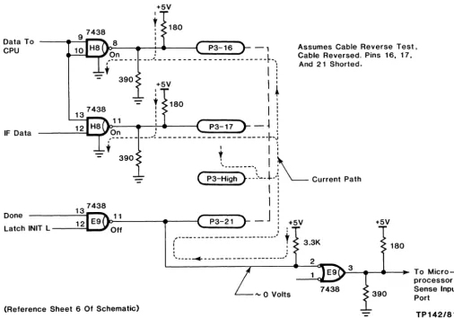
One unique feature of the I-Bus cable is the ability of the master controller to diagnose a cable that has been installed backwards. Pins 1 through 13 are all connected together to ground on both the controller module and the interface module. If the I-Bus cable is installed incorrectly, all the signals (pins 14 through 26) will be shorted together instead of all the grounds on pins 1 through 13. Refer to Figure 3-20. During the cable reversal test, the 8085 asserts Data-To-CPU and IFDATA lines to provide a sufficient current sink. The IDONE signal is asserted, at this time, by E9-11. The 8085 looks at IDONE through E9-2. If the cable
is backwards, it will be low. If the cable is installed correctly or is missing, it will be high.
IIF ROY L A4 SEL IIF STAT / Flags L SEL IIF SR/Pulser L R/WC Ready 10/M Ready L Watchdog Time Out L
(Reference Sheet 2 Of Schematic)
PUP
H7 3
CLK
Reset L 13 11
Reset Trap L 12
Figure 3-19. READY Hardware Logic
Ready
11 S F5 14
J Q 9 Ready
13 Time
K Out L
12 >
15
+5V
I
r
180Data To - -___
-'-I,...,.
8 ICPU 10 P3-16 - ,
IF Data
...----._, On :
,---- -- ----,---
---
--
--
---~-,t i l
- 390 +5V
I :
:
I
t
7438
13
- r
180I
!
11 I I I
12 I O - - -...
-!-: .... ---(
P3-17 - -i :Assumes Cable Reverse Test. Cable Reversed. Pins 16, 17,
And 21 Shorted.
---"':"='-Lo..J,9!:' ____ ___ .l __________ ____________ +~j
- t
390t _______ .
::~
• I
_ ( P3-High }--~.--!.-'\ Current Path
Done
Latch INIT L --~~" Off
P3-21
r
I :
I
_J
.
, I: +5V
,'--- ---- --- -- --- _____ .J
t
I •
,
.
, ,
' ... ___ --+ - ___________ --- ___ ... .-1
+5V
3.3K 180
2
>-=-3~"""'''''''--l~ To Micro--....:....aL-' processor '" 0 Volts 7438
[image:41.617.54.561.44.398.2](Reference Sheet 6 Of Schematic)
Figure 3-20. Cable Reversal Test Logic
Controller Interface To The I-Bus
390 Sense Input Port
TP142/81
There are six input lines into the controller from the 26-pin I-Bus cable. Two of the lines, IFDATA Land IERROR L, are bidirectional. The IDMA mode, I12BM, IFRDY, and !ERROR I-BUS lines are fed into the 8085 via the tri-state buffer at location D8. These lines may be read by doing an I/O read operation at the If STAT/FLAGS port (addresses AO through AF or BO through BF).
The IF INIT input is used to clock the latched INIT flip-flop at F8. This FF may be read at any time after it has been latched. This allows an INIT to. occur while the 8085 is engaged elsewhere. The INIT can still be recognized later.
The IF DATA input is fed into the interface shift register and into the parity check circuit. The parity check circuit performs a parity test on all shifted data from the interface. The parity check circuit is also driven by the PULSER circuit of the 8085. This allows the parity check circuits to be tested by forcing and clearing the parity error, and checking that the circuit output is valid.