TECHNICAL MANUAL
IIGDCDuGOGGOGODD'8D06Dlllllllllllnfi~' 1 Ii • S II I t 1.11 IllI 1 ... 11 11111111 121 . . . " . , .
1111111111111111111111111"
~-~5D
L~"'n "'E~nf'"
ZZZZZ22ZZZZZZZZZZZ2ZZZ·
3133333131l13l3"~'
4UU'" 5 5 5 5
55F
11
© DOCUMATION. INCORPORATED. 1971 Contenls of this manual may not be repro-duced in whole or in part without written permisllion of Documalion. Incorporated.
II
I
I I
CDCUMATIDN
IMPORTANT NOTICE
THIS TECHNICAL MANUAL IS SUPPLIED
WITH DOCUMATION CARD RFADER SERIAL
NUMBER
THI S MANUAL SHOULD· REMAI N WI TH THA T
Paragraph 1.1 1.2 1.3 1. 3.1 1. 3.2 1. 3. 3 1.4 1. 4.1 1. 4.2 1. 4.3 1. 4. 4
1. 4.5
1. 4. 6 1.4.7 1.4.8 1.5 2.1 2.2 2.3 2.4 2.5 2.6 2.7 2.8 3.1 3.2 3.3 3.4
TABLE OF CONTENTS
SECTION I DESCRIPTION
INTRODUCTION SCOPE
DESCRIPTION AND DATA Purpose and Use General Operation Description
C-150 OPTION Record For'mat Data Format
Parity bit Stop Bit(s)
Data Format Option Selection Control Characters
Data Rate
Tni-o't"fc:lno 'HtT1'\l'll D1'\r1 (""'1£'>1'\1'\0"#-"''''
.LL.&.u""..a.. .... ILA.""""'" ...,.LO~~U.L c..~.I...I.'-" '-'V.LLl..1.V"",,,V.L TECHNICAL CHARACTERISTICS
SECTION II
INSTA LLA TION AND OPERA TING INSTRUCTIONS
INTRODUCTION
UNPACKING PROCEDURES INSTALLATION
INTERFACE AND POWER CONNECTORS CONTROLS AND INDICATORS
PREOPERA TIONA L PROCEDURES NORMAL OPERATING PROCEDURES MINOR MA LFUNCTIONS
SECTION III
OPERATOR MAINTENANCE Page 1-1 1-1 1-1 1-1 1-2 1-2 1-2 1-4 1-5 1-5 1-5 1-6 1-7 1-8 1_Q
..L v 1-9 2-1 2-1 2-1 2-1 2-4 2-4 2-4 2-4
INTRODUCTION 3-1
PREVENTIVE MAINTENANCE 3-1
GENERAL PREVENTIVE MAINTENANCE TECHNIQUES 3-1
Paragraph 4.1 4.2 4.2.1 4.2.2 4.2.3 4.2.4 4.3 4.3.1 4.3.2 4.3.3 4.3.4 4.3.5 4.3.6 4.3.6.1 4.3. 6.2 4.3.6.3 4.3.7 4.3.8 4.4 4.4.1 4.4.2 4.4.3 4.4.4 4.4.5 4.4.6 5.1 5.2 5.3 5.3.2 5.3.3 5.3.4 5.4 5.5
SECTION IV
PRINCIPLES OF OPERATION
INTRODUCTION
BLOCK DLAGB_AM DESCRIPTION Timing and Synchronization Pick Action
Data Detection Data Storage
DETAIL FUNCTIONAL DESCRIPTION A C Power Distribution
DC Power and Signal Distribution Reader Control and Error Logic
1. 2 MHz Oscillator and Three Phase Generator Pick and Pinch Functions
Timing and Synchronization Synch Control Logic
Wide Strobe Control Logic r'nllntt:l1" r'nntl"nl T.nn-tn
~~~~v~_ --....,~~..,-....,~ ... "b.L ...
Data Detection and Storage
Data Handling and Timing Summary
" COMMUNICATIONS BOARD, BLOCK DIAGRAM DISCUSSION
Data Handling Timing
Transmitter/Receiver" Interface Driver/Receivers Received Character. Decoder Operation
SECTION V MAINTENANCE
INTRODUCTION REQUIRED TOOLS
ACCESS FOR MAINTENANCE Front Panel Removal Rear Panel Removed Top Cover Removal Bottom Cover Remova 1 TROUBLE SHOOTING
PICK AND FEED ADJUSTMENTS
Paragraph
5.5.1 5.5.2 5.5.3 5.5.4
5.5.6 5.5.7 5.5.8 5.6 5.7 5.8 5.8.1 5.8.2
Throat Knife/ Ramp Adjustment Card Guard Rail Adjustment Card Stop Action Adjustment Picker Assembly Adjustment
Optical Switch Assembly (Pick Sensor) Adjustment
Track Drive Belt Adjustment Picker Drive
Picker
MAGNETIC PICKUP REPLACEMENT MAGNETIC PICKUP ADJUSTMENT
READHEAD AND LIGHT STATION REPLACEMENT Read Head
Light Station
SECTION IV SCHEMATICS
SECTION VII PARTS LIST
Page
5-8 5-9 5-10 5-11
Figure 1-1 2-1 2-2 2-3 2-4 3.-1 3-2 3-3 ·4-1 4-2 4-3 4-4 4-5 4-6 4-7 4-8 4-9 4-10 4-11 4-12 5-1 5-2 5-3 5-4 5-5 5-6 5-7 5-8 5-9 5-10 5-11 5-12 5-13 6-1 6-2 6-3 6-4 6-5 6-6 6-7 6-8 6-9 6-10
LIST OF ILLTJSTRA TIONS
Card Reader, D-150 Series
Unpacking the D-150 Card Reader Installation Requirements
Interfa.ce Ca.ble
Controls and Indicators Card Reader 3/4 Front View Card Reader Bottom Interior View Card Reader Top Interior View Block Diagram
Timing Relationship For Standa~rd Punch Card
Control and Error Logic, Simplified Oscillator and Three Phase Generator
Pick and Pinch Control Functions, Simplified Timing and Synchronization, Simplified
Block and Timing Diagram, Data Amplifiers and Inverters Block and Timing Diagram, One Dark and One Light
Block and Timing Diagram, Data Registers and Data Drivers Circuit Cha.ra.cteristics
Interface Timing for D series Readers Communication Board, Block Diagram Card Reader, 3/4 Front View
Throat Knife/Ramp Adjustment Lift Rear Guide Rail Adjustment Use of Guide Rail and Template Card Stop A ction Check
Card Stop Acceleration Adjustment Card Reader Bottom Interior View
~icker Assembly Adjustment
Optical Switch Assembly Adjustment Track Drive Belt
Picker Drive Belt Picker Belt
Magnetic Pickup Adjustment AC Wiring Diagram
Card File Assembly
D-150 PC Card Interconnect Wiring Diagram DC-150 PC Card Interconnect Wiring Diagram Power Supply Schematic (115 VAC 60 Hz) Power Supply Schematic (220 VA C 50 Hz) D-150 Card Assembly
D-150 Logic Diagram C-150 Card Assembly C-150 Logic Diagram
Figure Page
7-0 Figure Reference 7-3
7-1 Main Frame Assembly 7-4
7-2 Card File Assembly 7-5
7-3 Power Supply Assembly 7-6
7-4 Control Panel Assembly 7-7
7-5 Connector Panel Assembly 7-8
7-6 Front Panel Assembly 7-9
LIST OF TABLES
Table Page
1-1 Technical Characteristics 1-10
2-1 Interface Connector Pin Assignment 2-6
2-2 Controls and Indicators 2-8
2-3 Pre-Operational Procedures 2-9
2-4 l\.T,...,.,,....'V'V'\nl r'\'I""'-I"'\."",n4-:r"I.'" 0 "10
J.'V.LJ.J.J.Q,.L '--'pv.LQ,l,..LV.l.l " , - 1 . " ,
2-5 Minor Malfunction Correction 2-14
3-1 Operator Maintenance Check Lis t 3-2
5-1 Required Tools 5-2
5-2 Fault Isolation Chart 5-5
SECTION I DESCRIPTION
1. 1 INTRODUCTION
1.2
1. 2.1
1. 2.2
1.3
1. 3.1
This nlanua.l contains interface, operational and maintenance instructions for the Documation Incorporated Series D-150 Card Rea.ders. (Figure 1-1). In addition to these instructions there is an identification table of parts replaceable by the operator/user.
SCOPE
The material contained in this instruction manual is directed primarily toward an equipment operator with limited electro-mechanical skill.
This manual consists of seven sections as follows:
a) Section I.
c) Section III.
d) Section IV.
e) Section V.
f) Section VI.
g) Section VII.
Introductory information, electrical description, optional features, and technical characteristics.
Servicing and insta.lla.tion, operating instructions.
Preventive maintenance, lubrication, adjustments and trouble analysis.
Principles of operation.
Maintenance.
Schematics.
Parts list.
DESCRIPTION AND DA TA
Purpose and Use
The Series D-150 Documation Incorporated card readers are designed to con-vert information from punched data cards to an electronic signal,
1. 3.2
1.3.3
General Operation
The Basic Card Reader is designed to read standard ANSI 12-row, 80 column punched cards. Up to 400 punched cards are loaded in the input hopper. The cards are separated from the stack sequentially, using a side friction picking technique, and moved past a phototransistor read station, where the data is recognized in a serial column-by-column manner. The cards a.re then deposited in the output stacker in the same order as they were originally put into the reader. The reading cycle is externally controlled for single card selection or continuous run.
Description
The D-150 Series card readers are specifically designed for continuous duty operation in adverse operational environments. The chassis is of heavy duty construction and all components have been chosen to provide for reliable per-formance, with minimum maintenance. The side friction picking technique will allow end damaged and warped cards to be handled smoothly and quietly. The electronic controls are implemented by standard integrated TTL logic modules on a single printed circuit card to minimize service problems. Infra-red light-emitting diodes and phototransistors are used at the read station to insure long-term reliability in the basic model.
The two models described in this manual are:
a) D 150 Punched Card Reader 12-bit parallel output.
b) DC 150 Punched Card Reader with serial RS-232C output.
1. 4 C-150 OPTION
The EIA standard RS-232C output, on Model DC-150 is provided by the addition of another printed circuit card incorporating the necessary logic circuit ele-ments to convert the data from a parallel to a serial format and provide the required features to permit the D-150 to be used as a terminal device. The C-150 board contains the most up-to-date TTL and MaS circuitry on a standard 150 series sized card. The DC-150 may interfa ce with any 103 or 202 Series Modem for telephone line communication. The reader may be equipped with the appropriate interface to communicate over lines, up to one-half mile of twisted pair.
The following features are either hardwired or switch selectable. See appendix A for the features incorpora ted in this unit.
a) Converts Hollerith to one of the following:
b)' Complete record (card) storage for retransmit capability.
c) Transmits data in a record format.
d) Customer selected codes for the following control functions:
1) Start of record (SOR)
2) End of record (EOR)
3) Reader ready 4) Hopper empty
5) Pick one card
6) Resend last record
7)
Start auto run mode8) Stop au to run mode
Note: ATJY of the above ei~ht (8) codes must be specified upon order
placement.
e) Six standard switch selectable baud rates:.
1) 110 Bits/Second 2) 150 BitsiSecond 3) 300 Bits/Second 4) 600 Bits/Second 5) 1200 Bjts/Second 6) 2400 Bits/Second
f) Swi tch selectable data format:
1) Parity or no parity 2) Odd or even parity 3) One or two stop bits
4) 5-8 Data Bits/data character
*
g) Four different signal interface driver/receiver configurations:
1) EIA. RS232-C (for modem use)
2) Differential (for long distance twisted pair up to 2500 feet) 3) Positive True (for short distance and non-modem)
4) Ground True (for short distance and non-modem)
1. 40 1 Record Format
The record format for punched 80 column cards is fixed at 80 data
characters per record. Each record is "framed" by special characters
referred to as START OF RECORD (SOR) and END OF RECORD (EOR).
These two special characters are customer assigned prior to assembly since they are hand-wired into the character generator. However, these
character codes may be field changed. Most common of framing characters are: Line Feed (LF) for start of record, and carriage return (CR) for end of record.
SOR EOR
~---HO data characters ~
~ L---~f sr---~ ~
80 Column Punch Car9 Record (82 Character)
The record format for optical mark cards is the same as that of punched
*
cards, except that the data portion is variable in length. The number of
clock marks existing On the edge of this type of card is the number of data
characters in the record. The SOR and EOR are the same as described
in 1. 5.2.
SOR EOR
~~I---_O to 80 d:taschar. * ~--_u_-rL
Optical Ca rd Record
1. 4. 2 Data Format
1.4.3
1. 4.4
Each character, whether it be a data character, a framing character t or
any other special character~, will have the following general format when
serially being transmitted.
I
j4--Character~
I
I I
~
~
:<;:I~I:"J
~
~
00:I~ ~
GENEHAL~, r ~ ... ...
I
'"' 'J ~ Co DATA FOH.1\IA T
I~I
i~ ~ ~
IO:I~I~I
JW~I
II
rL
Each character transmitted always begins with a sync (or start) bit. Immediately following the sync bit is the data character. Thi s character may be five, six, seven or eight bits in length, depending upon the type of coding used. The data length is switch selectable. For example,
if ASCII were used, the data character would be seven bits in length.
Parity Bit
The parity bit is the bit which follows the data character. The purpose for this bit is error detection. The parity bit may have any of the fall owing -forms:
a) Odd Parity: The parity generator inserts a bit (either A "1" or A
"Oil) to make the sum of the "1" 's in the data bits AND parity bit
an odd number. In other words; if the number of "1" t S in the data
character is even, then. t;4e parity bit will also be a "1", causing the sum to be odd.
b) Even Parity: The same as odd, only the sum of the bits will be even.
c) Mark: The parity bit will always be an "1". (For 7 bit codes or less).
d) Space: The parity bit will always be a "0". (For 7 bit codes or less).
e) No Parity: There is no parity bit, and the stop bit (s) immediately
follow the data character.
Stop Bit (s)
1. 4.5 Data Format Option Selection
The number of data bits, the status of the parity bit, and the number of stop bits are all switch selectable on the C150 communications board. To control these functions there is a miniature cluster switch with eight (8) sections (83). Each section is a separate sWitch and the sections are all numbered.
Sections 1-5 have the following functional control:
Section Position Function
83-5 ON Parity check and generator ON
83-5 OFF Parity check and generator 0 FF
83-1 ON ODD Parity
83-1 OFF EVEN Parity
83-4 ON ONE stop bit
83-4 OFF TWO stop bit
The on position is selected by depressing the black dot on the side of the
_ _ _ 1 ________ ~L_l_
l.Vl,;I\.~l.- ~W1Ll,;U.
83-2
ON OFF ON OFF
83-3 Bits/ Character
ON Five
ON 8ix
OFF 8even
OFF Eight
Note 1
If odd, even, or no parity is selec~
ed, then the receiver also checks the same parameters as the transmitter generates. The same is true with the number of data and stop bits.
Note 2
1. 4.6 Control Characters
There are two types of control characters used in this system. The first type is those characters which are transmitted to the receiving end device from the card reader in indicate some condition oiher ihan data. Two of these "special" characters have already been mentioned, (SOR and EOR). The other two special characters of this first type are also customer selected (coded) and they indicate the following conditions:
a) Ready'
When the reader "START" pushbutton is depressed indicating that the reader is ready to transmit, a special character is sent to the end device to indicate this condition.
b) Hop~er Empty
Imm.ediately after the last card in a deck has been transmitted, there will be another special character generated and transmitted to the end device to indicate the hOppel" eIIlpty and the end of transmissiun thit) character is also customer coded.
Data ~
£r
Char.-I~
J
i
~l---'
~
Last Record.1
,The second type of control signal is those which are sent to the card reader from the end device. There are four different commands which perform the following functions and are all customer coded:
a) Pick
Each time a coded character assigned to be decoded as pick it is received by the reader, the reader will pick, read, and transmit ONE complete card.
b) Resend
c) Auto Run (or Auto Start)
If the user does not care to issue a pick command to initiate each record, a coded character may be sent to the reader to automatically send
record after record. The reader will not stop until the hopper goes empty or the reader receives an AUTO STOP command. A motion check or read check will also stop the auto read.
d) Auto Stop
A coded character sent to the reader to take it our of the Auto Run mode.
1.4.7 Data Rate
The rates at which data is transmitted are all universally accepted baud ra~es.
There are presently six standard baud rates, all switch selectable, incorp-orated into the communication board. These are 110, 150, 300, 600, 1200 and 2400 bits per second. There is an 8-section cluster (S2) switch used to select the desired baud rate. Each section is a separate numbered
swi tch selecting a unique baud rate. There are two spare sections which
may be used to select customer special customer special baud rates. ONL Y
ONE SECTION IvIDST BE ON AT ONE TIIvIE.
S2-4 - 110 B/S S2-6 - 150 B/S S2-5 - 300 B/S S2-3 - 600 B/S
1. 4. 8 Interface Signal and Connector
S2-2 - 1200 B/S
S2-1 - 2400 B/S S2-7 - Spare S2-8 - Spare
The serial interface is composed of three types of signal lines:
a) Data Lines
b) Communications control lines
c) Signal and protective common return lines
All these lines are as outlined in the EIA-RS232-C Specification and are as
listed below.
a) Transmitted data (data out) (BA) b) Received data (data in) (BB)
c) Request to send (control) (CA)
d) Clear to send (control) (CD)
f) Data set ready (control) (CC)
g) Signal ground (common return) (AB)
b) Protective ground (AA)
( ) - RS232-C circuit reference
The connector used by Documation for the serial interface is a universally accepted 25-pin female connector. The pin assignments are again as per the EIA RS232-C specification and are as follows:
Pin No.
1 - Protective Ground 2 - Transmitted Data 3 - Received Data 4 - Request to Send
1. 5 TECHNICAL CHARACTERISTICS
Pin No.
5 - Clear to send 6 - Data Set Ready
7 ~ Signal Ground
20 - Data Terminal Ready
Table 1-1 Technical Characteristics
CARD CAPACITY
CARD RATE
CARD TYPE
CONTROL
INPUT
Pick Command (PC)
OUTPUT
Data Lines and Interface Signal
POWER
SIZE: Height Width Depth Stacker
SHIp,PING WEIGHT
OPERATING ENVmONMENT Dry Bulb Temperature Relative Humidity Wet Bulb Temperature Thermal Shock
Altitude
STORAGE ENVIRONMENT: Dry Bulb Temperature Relative Humidity Altitude
Hopper/Stacker 400 cards
220 cards per minute
Standard ANSI 80 column card or Mark
Sense card or specified in para. 1.4
Demand feed, one card at a time under external program control. Continous run if Pick Command remains true.
Logic True 1 microsecond
-15 MaDC @ 0.8 VDC Max.
TTL Type 7417
I Source 2.2 MaDC
I Sink -15 MaDC @ 0.40 VDC Max.
103.5 to 126.5, 57 to 63 Hz, 165 VA
8.5 inches
11 inches (w/o stacker)
18.25 inches
8
inches45 pounds
50 to 100oF.
30 to 90% non-condensing
80oF. max.
15 of. per hour
1000 feet below to 6000 feet abcve
sea level
-25 to +1350F.
5 to 95% non-condensing
1000 feet below to 12,000 feet above
Table 1-1 Technical Characteristics (Cont.)
CARD STOCK
The card must meet American National Standard's Specification ANSI X3.11-1969, Specification for General Purpose Paper Cards for Information Processing.
PUNCH DATA
SECTION II
INSTALLATION AND OPERATING INSTRUCTIONS
2.1 INTRODUCTION
This section contains procedures for u~packing, inspecting, instaliing and
operating the Series D-150 card readers. Upon receipt of the unit, inspect the outside of the container and report any damage to the carrier immediately.
2.2 UNPACKING PROCEDURES (Figure 2-1)
Unpack the D-150 card reader as follows:
a) Remove tape and bands from cartons and open flaps.
~
b) Remove upper half of styrofoam inner container to expose card reader
and assessories.
c) Remove power cord,· hopper follower weight and operator's manual
from container.
d) Lift unit out of the container.
e) Unpack and attach stacker and card depressor to unit. (Attaching
hardware in plastic bag. )
Mter unpacking, inspect the exterior of the unit for any surface dalnage which may indicate probable damage to the interp.al electronic or electromechanical components. Report any damage to Documation Incorporated, P. O. Box 1240, Melbourne, Florida. Verify contents against shipping document.
2.3 INSTALLATION
2.4
2.4.1
Figure 2-2 illustrates the physical dimensions of the D-150 card reader which govern the placement of the unit. Place the unit as close as possible to the
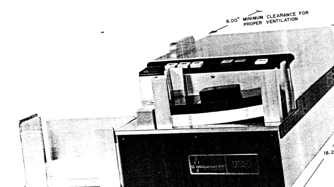
associated data processing equipment. Six inches minimum space should be
provided at the rear of the unit for proper ventilation.
INTERFACE AND POWER CONNECTORS
A 38-pin output connector provides access for all control, data and alarm signal lines. The output connector is ELCO part No. 00-8016-038-000-707 and
solder-1 REMOVE TAPE
AND BANDS
3 REMOVE ACCESSORIES
,
5 UNPACK STACKER AND PLASTIC CARD DEPRESSOR. ATTACH TO READER
(SEE FIGURES 1-1 " 1-3)
2 REMOVE UPPER STYROFOAM COVER
~
[image:22.872.58.742.88.472.2]MlNlMUM CLEARANCE FOR PROPER VENTlt.ATlON
type pins. A multiconductor cable must be prepared for the interface of the Card Reader and the Control Equipment. Figure 2-3 illustrates the interface
cable and table 2-1 lists the pin function assignments. Twisted pairs A \VG #22
color coded wires should be used for the cable fabrication. P2 for the interface cable should be a matching connector for the eXisting equipment. Refer to the table of technical characteristics for logic interface requirem"ents.
2.4. 2 The power connector is CORCOM part No. 6EFl. The mating connector is part
of the (supplied) standard accessory power cord BELDEN part No. 17250-C.
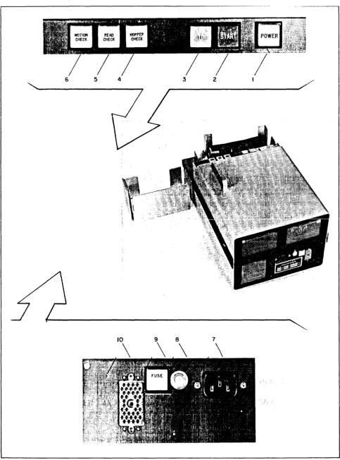
2.5 CONTROLS AND INDicATORS
Figure 2-4 "and Table 2-2 illustrate and list all the controls and indicators of the D-150. The operator should become familiar with their location " and function prior to placing the uni t in operation.
2.6 PRE-OPERATIONAL PROCEDURES . "
Table 2-3 lists' the necessary steps that should be performed prior to
operating the r~ader to insure that all controls. and monitors are functioning
properly: The steps constitute R complete pre-operaUorHll chpck of thp
"unit. If your unit is equipped with the C-150 'option, see Appendix A for
proper setting of Data Format selection switches and Data Rate switches.
2.7 NORMAL OPERATING PROCEDURES
The normal operating procedures listed in Table 2-4 are to be used as a guide for daily operation of the" equipment •.
2. 8 rvIINOR MALFUNCTIONS
,
During operation of the Card Reader, minor troubles may develop which can be remedied by the operator. The unit will automatically stop if a card
fails to feed, or be read, correctly, or the input hopper is empty. Procedures for correcting a minor malfunction are presented in Table 2-5.
CAUTION
~~---..:;;=---2.0FT---( NOMINAL)
3 4
QUAN. NO. DESCRIPTION MANUFACTURER
-1 1 Connector Assembly ELCO 00-8016-038-217-704
38 2 Contact Connector ELCD 60-8017··0513
1 3 Cable 19 PR #22 7/30 PVC 200V 10' ALPHA 1327/19
1 4 Connector Assembly (As required for existing equipment)
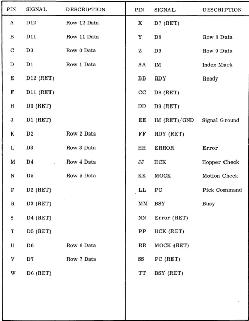
Table 2-1 Interface Connector Pin Assignment
PIN SIGNAL DESCRIPTION PIN SIGNAL DESCRIPTION
A D12 Row 12 Data X D7 (RET)
B D11 Row 11 Data Y D8 Row 8 Data
C DO Row 0 Data Z D9 Row 9 Data
D D1 Row 1 Data AA 1M Index Mark
E D12 (RET) BB RDY Ready
I
F
D11 (RET) CC D8 (RET)H DO (RET) DD D9 (RET)
J D1 (RET) EE 1M (RET)/GND Signal Ground
K D2 Row 2 Data
FF
RDY (RET)L D3 Row 3 Data HH ERROR Error
M D4 Row 4 Data JJ HCK Hopper Check
N D5 Row 5 Data KK MOCK Motion Check
P D2 (RET) LL PC Pick Command
R D3 (RET) MM BSY Busy
S D4 (RET) NN Error (RET)
T D5 (RET) PP HCK (RET)
U D6 Row 6 Data RR MOCK (RET)
V D7 Row 7 Data SS PC (RET)
[image:25.613.75.563.99.729.2]6 5 4 3 2
[image:26.617.55.539.73.725.2]~~---REF. 1 2 3 4 5 6 7 8 9 10
Table 2-2 Controls and Indica.tors (See Figure 2-4)
NAME
POWER
START
I
STOPHOPPER CHECK
READ CHECK
MOTION CHECK
AC RECEPTABLE
CmCUIT BREAKER
FUSE
RECEPTABLE
DESCRIPTION
White - Alternate action
Swi tch/indicator
FUNCTION
When lighted energizes drive motor and power supply
Green - Momentary action When lighted indicates reader
switch/indicator ready to receive pick command.
Red - Momentary action sWitch/indicator
Amber - Alarm indicator
When lighted, will override the pick command. Card reader will stop operation after card currently in track is read com-pletely.
When illuminated, indicates that the input hopper is empty. Pick motor will stop.
i .. A .. mber = Alarm indicator \Vhen illuminated, indicates that
Amber - Alarm indicator
Polarized AC
3A Main Power Breaker
1A Buss Fuse
Interface Connector
the card just read may be torn on the leading edge or have punches in the 0 column. Will cause the reader to stop.
When lighted, indicates the last card has not cleared the card track or a card has not passed the throat knife.
AC power input
Circuit protection when tripped a red band is expos ed. ,"Tait on minute, push to reset.
DC Power Fuse
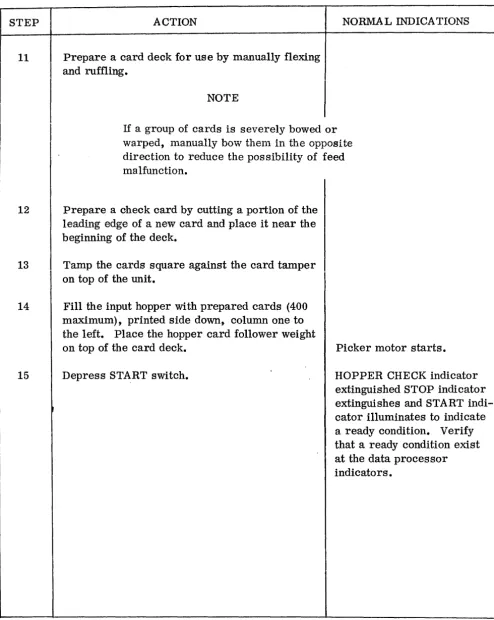
Tabie 2-3 Pre-Operational Procedures
STEP ACTION
1 Verify that the input hopper and output stacker
I
are free of foreign matter.2 Remove hopper card follower weight.
~
3 Wlpe InterIor of Input hopper and output stacker
with soft~ lint-free cloth.
CAUTION
NORMAL INDICA TIONS
I
DO NOT USE ANY CLEANING FLUIDS WHICH MAY DAMAGE PLASTIC OR RUBBER LIKE MATERIALS. ONLY A MILD SOAP SOLUTION SHALL BE USED
AS A CLEANING AGENT.
I
4 Clean the exterior of equipment and all plastic
surfaces covering the indicators.
5 Use a small soft bristle brush to clean dust
from the surfaces of the read station and card track area.
6 Plug in power cord at rear of uni t and· verify
that the power mains are of the proper voltage
and frequency. (115:t 11.5 VAC 60 Hz)
7 Verify that the circuit breaker is set by
push-ing bu tton in.
8 Connect AC power cord to the power outlet
9 Connect the interface connector between the
card reader and the data processor.
10 Activate POWER switch Indicator illuminates, main
drive motor on.
HOPPER CHECK indicator illuminates
i
I
Table 2-3 Pre-Operational Procedures (Cont.)
STEP ACTION NORMAL INDICATIONS
11 Prepare a card deck for use by manually flexing
I
and ruffling.NOTE
If a group of cards IS severely bowed or
warped, manually bow them in the opposite
direction to reduce the pos sibility of feed rna lfunction.
12 Prepare a check card by cutting a portion of the
leading edge of a new card and place it near the beginning of the deck.
13 Tamp the cards square against the card tamper
on top of the unit.
14
15
Fill the input hopper with prepared cards (400 maximum), printed side down, column one to the left. Place the hopper card follower weight on top of the card deck.
Depress START switch.
Picker motor starts.
HOPPER CHECK indicator extinguished STOP indicator extinguishes and START indi-cator illuminates to indicate a ready condition. Verify that a ready condition exist at the data processor indicators.
[image:29.617.69.563.113.732.2]Table 2-3 Prpo-()npor~Hnn~l - - - -J:'--- ... - ... _- - - --- -- \ - ---... PrnraponnrpoQ /(:nnt \
I
STEP ACTION NORMA L INDICA TIONS
16 Request the data processor operator to initiate Upon receipt of the pi ck
COln-a pick commCOln-and. mand the card reader wi 11 start
processing the card deek as
I
programmed until the check card (damaged card) is reached.START indicator extinguished. READ CHECK indicator
illumi-I
nates, STOP indicatorillumin-ates and the unit wili stop. Verify that the fault indications are present at the data proces-sor equipment.
17 Remove the check card from the stacker and START switch illuminates,
press the ST~-qT switch. READ CHECK indicator
-uishes, STOP indicator exting-uishes, and the card reader will
j rp~l1mp nro("p~~inp' thp - - - r - - ---0 ---- - - - ----("~rrk_
I
18 Apply downward finger pressure to the card ST ART indicator extinguishes,
follower weight to stall the feed action. MOTION CHECK indicator will
illuminate, STOP indicator illuminates and the unit comes to a stop condition.
The proper fault indicator lights at the data processing equipment.
19
,
.
Release pressure from the card deck and START indicator illuminates,
press ·the start switch. MOTION CHECK indicator
extinguishes, STOP indicator extinguishes and the reader will resume processing the card deck.
20 Allow the unit to complete processing the After the last card, the HOPPER
card deck. CHECK and STOP indicators
illuminate and the START indi-cator extinguishes.
21 Request that the data processor operator
[image:30.612.63.602.91.734.2]I
Table 2~4 Normal Operation
STEP ACTION
1 Verify that the input hopper and output stacker
are clean of foreign matter.
I
Remove input hopper card follower weight.2
3 Prepare the card deck to be processed by
'" !
.
~ :manua.lly flexlng and ru~fllng •
4 Tamp the cards square against the card tamper
on top of uni t.
5 Fill input hopper with the prepared cards (400
maximum), printed side down, column 1 to the left. Place the hopper card follower weight on top of the card deck.
6 Make sure the power cord is plugged in and
the interface cable is connected between the card reader and the control equipment.
7
8
At the Control Panel, press POWER switch/ indicator.
Press START switch/indicator
NOTE
NORMAL INDICATIONS
POWER indicator illuminates, STOP indicator illuminates, drive motor starts, pick motor starts.
STAR T indicator illuminates to signal that the unit is ready to begin operation.
,""_1-1_ n A "T _ _ _ _ _ 1 " _ _ _ _ L! _ _ , " ___ L '\ ,
~ ctUlt:: 4-':t J.~UJ.IHi:ll VjJt::J.-ctUVll \ vUllL. , .1
STEP ACTION NORMAL INDICA TIONS
9 Wait for the pick command from the Control Upon receipt of the Pick
Com-Equipment. mand the card reader will sta rt
I
I
processing the deck. On(~ cardI
at a time or continuous run as determined by the external program.
10
I
Monitor the check indicators for possiblemalfuncti ons.
11 To stop the unit before all cards are read, The unit will stop when last card
depress the STOP button. picked has been read. START
indicator extinguishes, STOP
indicator illuminates ~
12 To start the unit again press START button. The unit will continue
process-ing the cards. STO P indicator extinguishes, START indicator illuminates.
The card reader will stop when all cards have been read. HOPPER CHECK indicator will illuminate, STOP indicator will illuminate and the picker motor will stop.
13
,
Repeat steps 1 thru 5 and 8 thru 12 asrequired to process additional cards.
14 Upon completion of last run, depress
the POWER switch to remove power
from the unit. POWER indicator extinguishes.
NOTE
The reader may be operated without the hopper card follower provided there is at least one inch of cards
Table 2-5 IvIinor Ivlaiiunction Correction
INDICATION
1. Power indicator does not light upon
activation
a. Drive Motors Off
1)
CORRECTIVE ACTION
Verify power available at wall outlet and power cord connections seated properly.
, 2) Reset circuit breaker (CB1)
b. Drive Motors On
2. The unit starts processing the decks
upon activation of START switch.
1)
Check fuse (F1)2) Replace indicator bulb (DS1)
a. Data processor generating a pick
command or intern8.1 LOCAL/ •
b.
,
. REMOTE switch in LOCAL.
Data processor not generating a pick command and LOCAL/
Response normal
REMOTE switch in REMOTE. 1) Check that interface cable is fully seated
at the card reader and at the Data Proces-sor.
2) Check for damaged interface cable.
3. START indicator not lighted
a.
b.
POWER & STOP indicator
lighted
POWER indicator "ON" STOP indicator "OFF"
Depress START swi tch
Table 2-5 Mjnor Malfunction Correction (Cont.)
INDICATION CORRECTIVE ACTION
4. Unit halted:
a.
b.
c.
,
u.
STOP indicator "OFF"
HOPPER CHECK indicator "lighted' ,
Replace STOP indicator lamp. (DS3)
Refill input hopper.
Verify card follower weight is in place
READ CHECK indicator lighted 1) Check the last card in output stacker for
damage.
lighted
2) Duplicate as required and replace at
bot-tom of the input hopper.
3) Restart the unit.
_ "1 \
I J..} Check bottom card in input hopper for
damage or two cards stapled or clipped
together. If the card damage is mild,
SECTION III
OPERATOR MAINTENANCE
3.1 INTRODUCTION
This section contains maintenance information for the Series D-150 card readers. These units are of rugged construction and are designed to provide many hours of reliable operation, as such, preventive maintenance is the primary consideration.
3.2 PREVENTIVE MAINTENANCE
Preventive maintenance is work performed on equipment (usually when the
equipment is not in use) to keep it in good working order so that breakdowns
and needless interruptions in service are kept ot a minimum. The main obj ect is to prevent certain troubles from occurring.
3.3 GENERAL PREVENTIVE MAINTENANCE TECHNIQUES
3.4
3.4.1
a. Use a clean. dry. lint-free cloth or a dry brush for cleaning~ Tf necessarv.
except for electrical contacts, moisten the cloth or brush with a mild soap solution; after cleaning, wipe the parts dry with a cloth.
b. Tighten screws, bolts and nuts carefully. Fittings tightened beyond the
pressure for which they are designed will become damaged or broken.
c. Table 3-1 is a preventive maintenance checklist to be used by the
operator as directed. References i.n the ITEM column refer to paragraphs
in test which contain required detailed or additional information. It is
recommended that the table be reproduced and used as a weekly maintenance log.
INTERIOR CLEANING AND LUBRICATION
Every six month or 1500 hours of operation the top and bottom covers of the uni t should be removed and a detailed inspection and cleaning should
be performed. To remove the covers proceed as follows:
a. Remove the power cord and interface cable from unit.
b. Remove the four retaining screws from the top covers (figure 3-1 item 1)
with a 3/32" Allen wrench and remove top cover.
c. With the 3/32" Allen wrench, remove the six retaining screws (figure 3-1
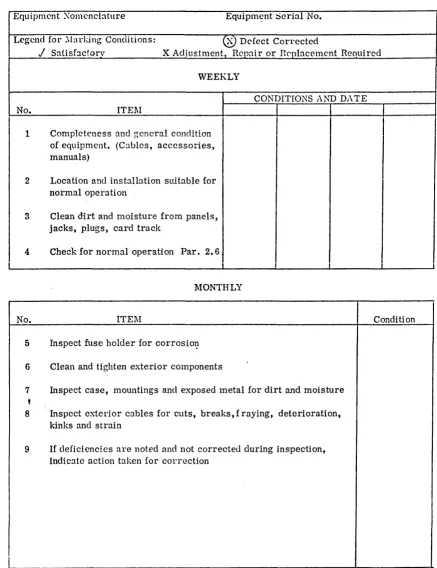
TABLE 3-1 OPERATOR IviAINTENANCE CHECKLIST
Equipment ~omenclature Equipm~nt ::ierial No.
Legend for ~Iark.ing Conditions:
Q9
Defect CorrectedJ
Satisf::lC!orv X Adjllstment, Repair or RC'pJacement RcouiredNo.
1
I
2WEEKLY
ITEl\!
Completeness und ~cncral condition of equipment. (Cables, accessories, manuals)
Location and installation suitable for normal operation
CONDITIONS A!'.1) DATE
3 Clean dirt and moisture from panels, jacks, plugs, card track
4 Check for normal operation Par. 2.6
MONTHLY
No. ITEM
5 Inspect fuse holder for corrosi0I}
6 Clean and tighten exterior components
7
,
Inspect case, mountings and exposed metal for dirt and moisture8 Inspect exi.erior cables for cuts, breaks, fraying, deterioration, kinks and strain
9 If deficiencies are noted and not corrected during inspection, indicate action taken for correction
[image:36.613.91.528.119.687.2]c.u
I
c.u
Figure 3-1 Card Reader 3/4 Front View
I (4 EACH)
3.4.2
3.4.3
3.4.4
With the machine exposed, check all visible moving parts for wear, noticeable defects, and excessive accumulation of foreign matter. Also check for loose pulleys and shafts paying particular attention to the drive pulleys and timing belts. Turn the driver power train by hand while making this inspection. Make a visual check of all polyurethane or rubber rollers for excessive wear or grooves. Report any parts that show excessive wear to your maintenance section.
Completely clean the unit as follows:
a. Using a small, soft bristle brush, remove all dust, card stock lint and all
foreign matter from the exposed surfaces of the unit. If a low pressure
(less than 30 psi) air hose is available, blowout the accumulated card chaff. A vaccuum cleaner may also be used to clean the unit if there is a large amount of accumulated dust.
b. Turn the unit upside down and clean the two polyurethane rollers in the card
transport area. To remove accumulated ink or other foreign matter,
dampen a cloth in soapy water and wrap it around the index finger. Hold
the finger against the roller surface and turn the driv.e belts slowly by
hand to rotate the rollers:
CAUTION
DO NOT USE ANY CLEANING FLUID ON SYNTHETIC OR PLASTIC SURFACES AS DAMAGE WILL OCCUR.
c. Use the same procedure as in (b) above to clean the picker wheel.
q.
Remove all foreign matter from the fan blades and the rear air screen.To clean the Picker and Pinch Roller Solenoid plunger and housing proceed as follows:
a. (Refer to figure 3-2) Using your thumb and forefinger, exert downward
pressure on the picker solenoid return spring (1) and remove it from the notched pin at the picker rocker arm.
b. Using the same procedure as (a) above, remove the lower end of the pinch
roller return spring from its retaining pin (2).
c. Disconnect the picker solenoid electrical plug (item 3, figure 3- 2) from its
3.4.5
d. Remove the two retaining screws from the picker solenoid housing (4) ancI
pull the housing away from its plunger.
NOTE
In the following steps$ it'is not necessary to lubricate the solenoids or their plungers. Cleaning to remove accumulation of dirt is all the ma.intenance required.
e. With a clean, dry, lint-free cloth, wipe the interior of the solenoid housing
and the solenoid plungers until they are free from all foreign nlatter. Re-install all components except the pinch roller return spring.
f. Disconnect the pinch roller solenoid electrical connector from its jack.
g. Remove the two retaining screws that hold the pinch roller solenoid in
place (5), and pull the housing away from its plunger.
h. Clean the plunger and the solenoid interior and reinstall.
i. Reinstall the pinch roller return spring, insuring that it snaps into the
groove of the retaining pin.
Lubricate the drive and picker motors (figure 3-2) as follows:
CAUTION
DO NOT OVER OIL THE MOTORS. THIS COULD CAUSE DETERIORATION OF THE INSULATION IN THE FIELD WINDINGS AND MOTOR FAILURE.
a. Every 4, 000 hours or yearly, whichever comes first, add 3 to 4 drops of
SA E 20W non detergent oil to each of the two oil points of the main drive motor (6) and the picker motor (7).
b. Wipe any oil spill from the unit to avoid accumulation of dust.
3.4.6 Clean the interior of the unit top and bottom covers and reinstall on the unit.
3.4.7 Reinstall the reader in its operating configuration and perform a pre-operational
7 5 3 4 4
6 OIL HOLE UNDER DEFLECTOR PLATE
6
CARD DEPRESSOR ATTACH ING SCREWS
LOCAL / REMOTE SWITCH
SECTION IV
PRINCIPLES OF OPERATION
4. 1 INTRODUCTION
This section contains a block diagram discussion of the card reader, a detail functional description and functional diagrams to enable the service personnel to familiarize themselves with the unit operation.
4.2 BLOCK DIAGRAM DESCRIPTION
4.2.1
4.2.2
The block diagram for the D-150 and the DC-150 card readers is shown in figure 4-1. The description that follows applies to both readers since the reliable recovery of data from cards passing down the card track is accomp-lished in the same manner.
Timing and Synchronization
The heart of the card reader electronics is the control and sync logic, where
the internallogic timing and the movement of the card past the read station are
synchronized to enable accurate sequential interpretation of the data on· the card •. Primary logic timing is established by a 1.2 MHz oscillator and the associated three phase clock logic, whose outputs are used to shift, store and control other timing operations. Card movement speed is established by the hysteresis synchronous drive motor. Synchronization is accomplished by a notched ferrous timing disc attached to one of the drive roller shafts. As the timing disc rotates, a reluctance pickup senses the movement of the disc's notches past the pickup producing timing signals. These signals are used by the Control and Sync Logic to generate Data Strobes (CSDS) for each of the 80 . columns of the punched card.
Pick Action
CONTROL PANEL a
STATUS INDICATORS CONTROLS AND INDICATORS
PICK COMMAND FROM EXTERNAL SOURCE
'f
..
PICK FRICTION~
RIVER -~ DRIVE1 - - - - PICK PICK
-0
- SOLENOID - - - ..
..t::\
PICKER~MOTOR
LED
Ie ,
~CC DRIVER -.--~ PINCH ROLLER PINCH PINCH - - - ••
0
OPTICAL SWITCH PICK SENSOR
HOPPER EMPTY SWITCH
MAGNETIC PICKUP
,,0
€),;
DRIVE MOTOR LIGHT STATION .---1~
? INTERNAL CLOCK TIMING STROBE GENI!RATOR DATA SE"SORSPINCH COMMAND _
r/JB ...
q,C
..
ct>o
CI ... HOPPER EMPTY
TIMING SIGNAL
-ONE DARK ROW 12
ROW II
ROW 0 ...
ROW 9
CONTROL AND SYNC LOGIC
,~
DATA BUFFERS
- SOLENOID ... TO DRIVE MOTOit
MOT ION CH ECK READ CHECK
HOP PER READY
..
READYr-__ 8_U_S_Y ________________________________ • ___ ~
INOEX MARKS DATA RE SET
DATA ENABLE
,
ON E LIGHT
... _ ...
,r
DATA REGISTER-..
DATA OUTPUT DRIVERS0-9 ...
TO EXTERNAL EQUIPMENT OR C-I'O BOARD
4.2.3
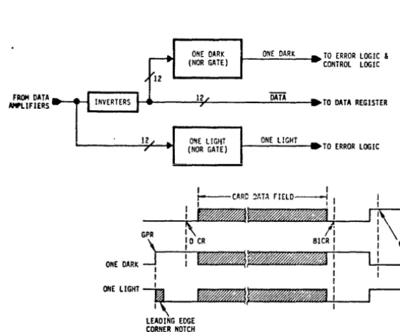
The Read Station and pick sensors utilize phototransistor to read the card's hole pattern and to monitor the card's movement. When a card is pinched and moved into the card tra.ck, the leading edge interrupts the light to the Read Station. This produces a ONE DARK signal that is used by the Control Logic to generate a Good Pick Reset (GPR) which initializes the synchronization of the card's movement through the Read Station. A Column Counter then counts columns via the Control and Sync Logic as the card moves past the Read Station, thus synchronizing the mechanical card movement with the electronic circuits. The Column Counter generates a DARK CHECK at Column 0 and a Light Check at Column 84. Figure 4-2, Timing Relationship for Standard Card, shows these check positions. These checks provide a quality check on both the Read Station and the mechanical card movement.
Data Detection
As the card passes between the Light Emitter Diodes (LEDs) of the Light Station and the Phototransistors of the Read Station the light and dark conditions are
sensed and amplified by the Read Station's phototransistors $ The light (punched
hole) and dark conditions are converted to electronic signals at the Phototran-sistor's emitters and used to drive the Data Amplifiers and Inverters. Output of the Data Amplifiers and I.nverterspass through the all Light/all Da.rk in-verters and provide detected data to the .Data Register.
I I GPI! i i NOTES:
(I) DASHED LINES INDICATE PSEUDO HOLES IN CARD. (2) DC = DARK CHECK
LC = LIGHT CHECK GPR = GOOD PICK RESET
(3) HOLE SIZE EXAGGERATED FOR EXPLANATION.
a) HOLE SIZE = .055 IN. b) WEB SIZE = .032 IN.
r' r'
0--"
..
_---I I I II I I I
LJ LJ _ _ "" _ _ '. _ _ ..
"-0
r, r, I I I I 1 I I I r-,I I I I I I 1
. . _ LJL.J JLJ
o 01 I
I I I I I I I I I I I I I I DC
80 81 112 B! 1114
LC
CARD MOTION
4. 2. 4 Data Storage
To accomplish Data Storage, the Control and Sync Logic sends Synchronized Data Strobes (CSDS) to the Data Register at predetermined punched column positions. Data Storage includes Data Drivers that provide buffering between the Data Register and the interface lines or the communications electronics in the DC-150 model.
4.3 DETAIL FUNCTIONAL DESCRIPTION
The foiiowing gives a detailed, functional description of the D-150 Card Reader. The description is designed to give the reader an in-depth understanding of how the Card Reader works. The reader should familiarize himself with the signal mnemonics used in the text description since it will aid in interpreting both
the description that follows and the logic &3chematics in Section VI~
4.3. 1 A C Power Distribution
Figure 6-1 illustrates the AC power distribution in all the D-150 series card readers.
AC power is brought in, to the reader, via the connector filter assembly (J1/FL1), which functions to suppress conducted RF interference. The power is then routed thru the main circuit breaker (CB1), the POWER switch (Sl), to a terminal board (TB1).
From TB1, AC power is run to the drive motor (B1), to the" pick motor (B2)
and to the +5V power supply via fuse (F1)~ In models equipped with the C-150
option, jumpers are provided in connector P8 to bring AC power for the .:J:.12V 'power supply required in thes e units.
,
4.3. 2 DC Power and Signal Distribution
4.3.3 Reader Control and Error Logic
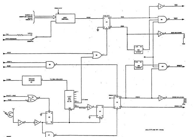
4.3.3.1 Reader control starts with the application of power to the reader. When the logic power comes up, the +5 VDC (VCC) applies to the Power On Reset Logic to generate PORe (Refer to FigUre 4-3).
POR is used to initialize the Pick and Pinch Logic and the timing and
synchron-izing logic. POR ORled with RESET to form POR + RESET to initialize the
Control Logic. The ~eader is now brought to the ready state by the operator
depressing the START switch, which activates the Reset Control Logic. RESET is routed to initialize the Pick Logic. and Column Counter and activates the
POR + RESET signal to the Error Logic. The Reset Control is designed to
ignore all RESET sw~tch signals while a read cycle is in progress.
Reader READY is signalled to the controlling device by the CONTROL Logic
when the START Switch is depres~ed provided HOPPER CHECK is not being
presented by the Error L-ogic. (All other Error Logic Check signals will be
reset by POR or RESET.) Reader RE~DY is indicated to the operator by the
START Switch illumin~ting. The controlling device can now begin a read cycle
by transmitting a PICK COMMAND to the reader. READY will be reset upon
receipt of any CHECK signal from the Error Logic or if the STOP Switch is
depressed by the operator and RESET INHIBIT is not present. The Stop Control Logic gates the STOP SWITCH CLOSURE signal with RESET iNHIBIT, preventing REA:py from ,being reset due to STOP during a card read cycle.
RESET INHIBIT, generated by the Res.et Contro~, is set by PCEN and reset by
CR, these Signals identify the beginning and end of a read cycle. The Stop Condition is indicated by the STOP switch illumina tinge
4.3.3.2 The Error Logic of Figure 4~3 contains the error/alarm detection circuits.
f Once a PICK CMD is accepted by the reader, the Error Logic is sampled at
intervals of card processing for error and reader conditions. These error/ reader conditions are referred to as CHECK CONDITION. Should a CHECK CONDITION occur, the reader READY will go low. The first test is Pick
Check. If a PSET is signa.lled, a Motion Check (MOCK) will be sent to the
controlling device. PSET will occur approximately 250 m sec after PICK CMD was received. Pick Check will be signalled to the operator by the MOTION
CHECK control panel indicator. If PICK CHECK does not occur, a read cycle
CII
KEADY
Cl
BE SW
oc.
POll
RESET
iiru
lI.ESET 1!o"llIBIT
1111 LIGHT
CHECIC
& ~
~:
V
!ll'SV . .
8 IlEADY
.
s i"iOPiiR 10K
I· I iEADTi5R
10K
9K
. . - - - 0 11K
) . : . - - - 1 IN
12 IIEAD CHECIt
Figure 4-3 Control & Error Logic (Simplified)
'I
LOGIC
~ro=,_,
)
TOCOSTROL PASEL INDICATORS
4.3.4
The Hopper Empty circuit senses closure of the Hopper Empty microswitch. This switch is located under the CARD STACK and senses when the last card has left the Hopper. Hopper Empty is signalled to the controlling device and READY is reset. Hopper Empty is signalled to the operator by the HOPPER CHECK indicator.
CR occurs next in the read cycie and samples the Light Check circuitry. A ONE DARK present at CR indicates a failed LED or phototransistor or excessive card slip in the read track. This error is signalled to the controlling device as
a. READ CHECK a.nd the READY line is reset. The reader control panel will
indicate READ CHECK.
All error conditions are cleared by depressing the START switch to generate the Reset signals.
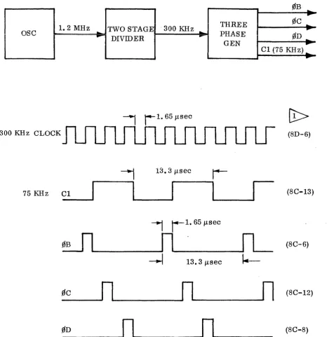
1. 2 MHz Oscillator and Three Phase Generator
The block diagram and timing diagram for the 1.2 MHz Oscillator and Three Phase Generator is shown in Figure 4-4. The oscillator provides a TTL com-patible 1. 2 MHz squar.ewave as an output. The 1.2 output is divided by a two stage counter and the counter's 300 KHz output used to drive the Three Phase Generator. The generator then divides the 300 KH z by four, generating signals that are gated as 0B, 0C, 0D and Cl as shown by the timing diagram of
figure 4-4.' 0B, 0C, 0D and Cl are used throughout the reader as a timing source.
4.3.5 Pick and Pinch Functions
Pick and Pinch functions are the same on all models of D-150 series card readers operational description as follows:
The unit will create a Power On Reset (POR) upon activation of the POWER switch which will normalize all the logic circuitry. The START switch will reset all error indications and the unit will be ready for operation.
When operating in the remote mode, an external program must generate the PICK COMMAND. Refer to figure 4-5.
When the external program pick command is received the pick control logic initiates the pick sequence by gating a clock signal (Cl) to produce the Pick Command Enable pulse (PCEN). The positive transition of the PCEN signal
will cause the logic
"0"
present at input "D" of the pick flip-flop, to betrans-ferred to output
"Q".
This output at "Q" energizes the pick solenoid via thesolenoid driver. The action of the pick wheel will move the bottom punched
card into the card track. Note that the output of the Pick F
IF
is also routed to-
..
1. 2 MHz
-
TWO STAGE ·300 KHz ... THREE 0C ......
ase
-
PHASE
0r-.
r
I
DIVIDER
GEN
I
Cl (75 KH:) :
-, r-1.
651lsec300 KHz CLOCK (8D-6)
~
13.3 Ilsecr-75 KHz C1
I
I
I
(8C-13)~
i 1 . 65 Ilsec~
n
IL
(8C-6)~
13.3 Ilsect.-0C
n
n
n
(8C-12)0D
n
n
(8C-8)~
NUMBERS INDICATE IC LOCATION AND PIN WHERE WAVEFORM CAN [image:49.615.74.541.143.624.2]BE MONITORED.
~
I
CO
PICK ooaUCAIID
IlroP
~roPI
.IIIT
15 lQIa
RF.lir.T. POIt
POWEROH
.aft' (NO ERIIORI
RMDY
T1111HO Cl
.EMOTE
DECADE DIVIDER
IIC
13
PINCH rlF
PICK
a.n'IIOL
• BIT
BIH
CTR nlTt
4C,3C 81T. JIlT.
pcp
4 . 1 _
DR ~3.2 m""
13
riCK FIF
PICK
~---
__
+-~-QI~~'--~~=-~~LF.~·~~~r
YOC
0/1 20
PlNeli
I III: II PINCH 50U:HflIII
I
vee
I'fI(CII rlr ..
!ALL rlr ARK "D"··TTPElJ
[image:50.794.54.718.54.526.2]If the card fails to reach the pick sensor in 250 milliseconds, the time delay
multivibrator will genera.te a logic "I" to enable the PSET gate. The other
in-puts to the gate come from the "Q" output of the Pick F
IF
and the clock (0D) sothat at the next positive clock transition, the PSET signal will be sent to the error control logi c to generate a Motion Check (MOCK) signal to stop the reader and light the alarm indicator. The error control logic will also generate the STOP signal to preset the Pick F IF and release the pick solenoid.
In normal operation, Power On Reset or activating the start switch, caused
flip-flop 4D-6 to preset. The Q output is used to inhibit an eight bit binary
counter and preset flip-flop 4D-8. When the card reaches the pick sensor, the optical switch goes dark and its output is conditioned and used to set flip-flop
4D-6, the Q output enables the 8 bit Binary Counter to start to count. To
establish the counting rate, the clock signal (Cl) is divided by a decade counter and the 7. 5 KHz signal is used to increment the eight bit binary counter. When
the count reaches 32 (4.26 M sec. after pick sensor), 'bit six is used to preset
the pick flip-flop and deenergize the pick solenoid. The
Q
output of the pickflip-flop is inverted and used as a pick command reset signal (PCR). At count 256 (all zeros, 34 M sec. after pick sensor), flip-flop 4D-8 is clocked and the
Q output conditions the data input of the Pinch F
IF.
The next positivetransi-4-;,.,....",...4! 4-),."" ,.,,1,...,.,.1~ INn\ 9~.:11 ~~ •• ..,,~ 1-1...~ A _ .. I- ___ L _-c Ll _ _ __ ! ___ L L"1! __ -C1 __ L _ __ J L-LVJ..l VL L-J..lv vLVv!).. \Y1LJ} VV.l.L.l va,UOI;; LUI;; '<t UULllUL Ul. Lllt:: 1111ll;U 11111-11U11 LU gu LU
logic "0" energizing the pinch solenoid, via the solenoid driver, causing the
picked card to move along the card track. The Q output of the pinch flip-flop
is used to inhibit the pick command when the pinch solenoid is active. If the
card fails to reach the read station in 250 milliseconds, the pinch set (PINSET) signal will be sent, causing the error logic to generate the STOP 2 signal. The STOP 2 signal gated with BUSY, will cause the Pinch FIF to clear, releasing the pinch solenoid. Under normal conditions, when the column counter gener-ates 8lCR the pinch circuits will be cleared for the next cycle.
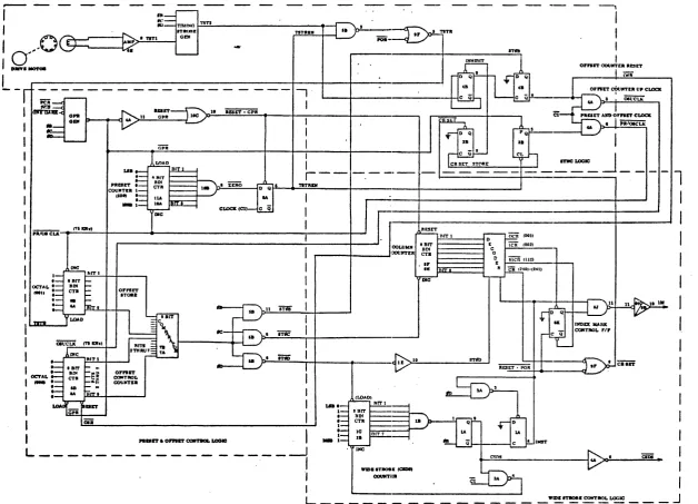
4.3. 6 'riming and Synchronization
-
----I
,
1
0
...
0
I .... __
L_
ua TaT"IN-.
I I Ir
-~-1~n_.a~~~-i ________ ~~ ________________________________ ~ ________ ~~
I
I
I I II
I
I
L __
OFFSET 170111I
- - - '
I
" I t i l l .I
• • I
• I
_ I
L ___ (LOADI
RTT I
DIT 7
INC
"DET
COWMN IXJ{1NTE"
• IF '" DCa
-- -- -- --
-~I
I I I OF"" COUNTER RESET~
I
_____
~L
___
~~IC_J,_
(11011
l
I
I
I
I
I
I
I,I
I
I
I
I
I
__ ____ ~~~)O~.---aroe~-..
I
[image:52.789.55.684.76.529.2]The GPR signal will last for the time interval between clock
0D
and next 0C(10 f..l sec) and will perform the following functions:
a) Load the Preset Counter (220 octal)
b) Enable the timing strobe (TSTR) gating structure to load the Preset store
at next TST2 signal (001 octal)
c) Loa.d the Offset Counter (000 octal)
d) Reset the Column Counter (000 octal)
e) Enable the Preset/Offset clock (PR/OSCLK)
4.3.6. 1 Sync Control Logic
The Sync Control logic (figure 4-6) provides data readout synchronization from the timing disc. The timing disc is mounted on the same shaft as the first capstan roller. This capstan roller engages the card as it is pinched and thereafter determines the speed at which the ca.rd will be moved through the card track. The asynchronous card pick and pinch sequence causes the card to arrive at the read station at an arbitrary time in relation to the timing disk. The edge of the ferrous alloy timing disc is provided with gear-type serrations such that two flux reversals occur for each column of data on the card track. These are sensed by the magnetic pickup and its associated amplifier to produce two TST1 signals for each column of data.
The TST1 signals produced by the timing disc pickup amplifier are gated with the internal logic clock to produce the TST2 signals as positive-going, 13.3 microsecond output pulses that are phased to 0C of the three phase clock.
From figure 4-2 it can be seen that the first one-quarter inch of a punched card, (which contains no data per EIA standard) could have two data columns punched
into it. The reader logic assumes the presence of these columns as if they do
exist and they are called column 0' (first pseudo-column occurring after the leading edge) and column 0 (second pseudo-column).
When GPR occurs, the sync logic will be conditioned to gate clock signal (Cl) as a Preset and Offset clock (PR/OSCLK).
Since the leading edge of the card may arrive at the read station at an arbitrary time in relation to the TST signals, it is necessary to determine this "offset" so that later data column strobes generated from the occurrence of the TSTl
signals will continue to be offset by the same amount for all 80 columns of that
particular card. It should be noted that this offset interval between TST and the data column strobes will be different for each successive card, but is consta.nt within each card.
These circuits count and store the time interval between the TST2 signal and
the end of preset interval (i. e., beginning of pseudo-column 0'). If two TST2
signals occur before the preset timing is complete (as indicated by generation of ZERO), the second TST2 resets the Offset Counter and its counting begins
again (i. e., the shortest time interval between TST2 signals and end of preset
timing is always selected). This "offset" interval is the synchronizing point
that established the beginning of each of the remaining 80 data columns on that
particular card.
The initialization reset for the Offset Counter is produced by TSTR, which is generated by the first and/or second TSTR signal after GPR but before ZERO occurs. After the preset timing ZERO is produced, the PR/OSCLK, and TSTR circuits are inhibited until the next GPR is generated; however, the second, fourth, sixth, etc., TST2 signal after ZERO is used to produce the OSR and OSUCLK signals. These two signals enable the Offset Comparator circuits to
reproduce a time interval equal to the original offset count for each o(the 80
columns of data in a punched card.
The OSR signal, which is raised by the second, fourth, etc., TST2 signal after the ZERO detect point occurs, allow the Offset Counter to be up-counted by the OSUCLK signal from sync control. A seven-stage, parallel comparator circuit recognizes when this count has equalled the binary value stored in the
seven-,stage offset counter. This up-count interval is regenerated 80 times as the card
moves past the read station. Hence, by using this technique of reestablishing
the value of the offset interval at the beginning of each card, the 80 data strobes
are able to readjust for the arbitrary leading edge arrival.
The output of the comparator logic is used to generate a sequence of three pulses which actually initiate the various strobe actions. These are derived from the three phase clock as follows: STe>C occurs first, followed by ST(>D, and ST£)B (STe>B is used to reset the compare cycle).
4. 3. 6. 2 Wide-Strobe Control Logic
The Wide-Strobe Control logic is used to produce the index marker strobes (IMST) and the column storage data strobe (CSDS). The ST0D Signal, generated by the comparator logiC, presets an eight stage counter to a binary value