Kinetic Features of Reactive Diffusion between Sn–5Au Alloy
and Ni at Solid-State Temperatures
Yu-ichi Yato
*1and Masanori Kajihara
*2Department of Materials Science and Engineering, Tokyo Institute of Technology, Yokohama 226-8502, Japan
In order to examine microstructure evolution at the interconnection between the Sn-base solder and Au/Ni/Cu multilayer conductor alloys during energization heating, the kinetics of the reactive diffusion between a binary Sn–5 at% Au alloy and pure Ni was experimentally observed at solid-state temperatures. Sandwich (Sn–Au)/Ni/(Sn–Au) diffusion couples were prepared by a diffusion bonding technique, and then isothermally annealed at temperatures ofT¼433, 453 and 473 K for various periods up to 1057 h. During annealing, AuNiSn8and Ni3Sn4
compound layers are formed along the (Sn–Au)/Ni interface in the diffusion couple. The total thickness of the compound layers is expressed as a power function of the annealing time. The exponent of the power function is close to 0.5 atT¼453{473K, and equal to 0.7 atT¼433K. Therefore, volume diffusion is the rate-controlling process for the growth of the compound layers atT¼453{473K, but interface reaction contributes to the rate-controlling process atT¼433K. The growth of the compound layers occurs slower for the reactive diffusion between the Sn–5Au alloy and Ni than for that between Sn and Au, but faster for that between the Sn–5Au alloy and Ni than for that between Sn and Ni. [doi:10.2320/matertrans.47.2277]
(Received April 10, 2006; Accepted July 4, 2006; Published September 15, 2006)
Keywords: diffusion bonding, reactive diffusion, intermetallic compounds, bulk diffusion, solder, conductor
1. Introduction
Owing to high electrical conductivity, Cu-base alloys are widely used as conductor materials in electronic industry. When the Cu-base conductor alloy is interconnected with a Sn-base solder alloy, Cu–Sn compounds are formed at the interconnection during soldering and then grow during heating under energization conditions.1–9) Since the Cu–Sn compounds are brittle and possess high electrical resistiv-ities, the growth of the compounds deteriorates the electrical and mechanical properties of the interconnection. The Cu-base alloy is usually plated with a Ni layer in order to inhibit the formation of the Cu–Sn compounds, and the Ni layer is plated with a Au layer for improvement of the corrosion resistance. If the Au layer of the Au/Ni/Cu multilayer conductor alloy is very thin, however, the Au layer completely dissolves into the molten solder during solder-ing.10–15) As a consequence, the reactive diffusion between
the Ni layer and the molten solder occurs immediately after the complete dissolution of the Au layer, and then a binary Ni–Sn compound is formed at the interface. Such a compound will grow under the energization heating con-ditions and may also deteriorate the electrical and mechan-ical properties at the interconnection.
Chen and Chen16) experimentally observed the reactive
diffusion in the binary Sn/Ni system. In their experiment, sandwich Sn/Ni/Sn diffusion couples were prepared by a soldering technique and then annealed at temperatures between T ¼433 and 473 K. Their observation indicates that a layer of Ni3Sn4is produced along the Sn/Ni interface
in the diffusion couple during soldering and grows during annealing. The thickness of the Ni3Sn4 layer is nearly
proportional to the square root of the annealing time. Such a relationship is called the parabolic relationship. The para-bolic relationship implies that the growth of the Ni3Sn4layer
is controlled by volume diffusion. However, in the soldering technique, the Ni3Sn4 layer with a certain thickness is
formed during soldering before annealing. Therefore, it is not so easy to distinguish the growth rate during annealing from the formation rate during soldering. Consequently, the soldering technique is not appropriate to observe the growth behavior of the Ni3Sn4 layer during annealing at solid-state
temperatures.
The reactive diffusion in various binary and ternary systems was experimentally observed at solid-state temper-atures using sandwich diffusion couples prepared by a diffusion bonding technique in previous studies.17–30) As to
the binary Sn/Ni system,17)Sn/Ni/Sn diffusion couples were
isothermally annealed atT¼433, 453 and 473 K for various periods. Along the Sn/Ni interface in the diffusion couple, Ni3Sn4 is produced as a layer at T¼453and 473 K but as
fine particles atT ¼433K. On the other hand, AuSn4, AuSn2
and AuSn layers are formed in Sn/Au/Sn diffusion couples at T ¼393{473K,18–20) and Cu6Sn5 and Cu3Sn layers are
produced in Sn/Cu/Sn diffusion couples at T ¼433{ 473K.21)In the binary Sn/Au, Sn/Cu and Sn/Ni systems, the total thickness of the compound layers is described as a power function of the annealing time. The exponent of the power function is mostly smaller than 0.5 at the experimental annealing temperatures. This indicates that grain boundary diffusion contributes to the rate-controlling process for the growth of the compound layers and grain growth takes place at certain rates in the compound layers. At each annealing temperature and time, the total thickness is about one order of magnitude smaller for the Cu–Sn compound layers than for the Au–Sn compound layers, but the thickness of the Ni3Sn4
layer is less than half of the total thickness of the Cu–Sn compound layers. As a result, the Ni layer acts as an effective inhibitor against the reactive diffusion between the Au/Ni/ Cu multilayer conductor and Sn-base solder alloys during energization heating after the complete dissolution of the Au layer into the molten solder.
When the Au layer of the Au/Ni/Cu multilayer conductor
*1Graduate Student, Tokyo Institute of Technology
alloy is sufficiently thick, however, the Au–Sn compounds are formed during soldering and then grow during energiza-tion heating.10–15)If the Au layer is uniformly depleted during
growth of the Au–Sn compounds, the Ni layer will be reacted with the Au–Sn compounds after complete depletion of the Au layer. In order to examine characteristic features of such a reaction, the reactive diffusion in the ternary (Sn–Ni)/Au system was experimentally observed at solid-state temper-atures using (Sn–Ni)/Au/(Sn–Ni) diffusion couples in a previous study.22)Here, the notation (A–B)/C indicates that
reactive diffusion takes place between a binary A–B alloy and a pure C metal at appropriate annealing temperatures. In that experiment, binary Sn–Ni alloys with concentrations of 1, 3 and 5 mass% Ni were used to prepare the diffusion couples by the diffusion bonding technique. The diffusion couples were isothermally annealed atT¼433{473K. Due to annealing, AuNiSn8, AuSn4, AuSn2 and AuSn layers are
produced along the (Sn–Ni)/Au interface in the diffusion couple. Also in this case, the total thickness of the compound layers is expressed as a power function of the annealing time, and the exponent of the power function takes values between 0.3 and 0.4. This deduces that the same rate-controlling process as the binary Sn/Au, Sn/Cu and Sn/Ni systems works for the ternary (Sn–Ni)/Au system. However, the overall growth rate of the compound layers is greater in the ternary (Sn–Ni)/Au system than in the binary Sn/Au system. This means that the reactive diffusion in the binary Sn/Au system is accelerated by the formation of AuNiSn8due to the
reaction of Ni with AuSn4atT¼433{473K.22)
If the Au layer of the Au/Ni/Cu multilayer conductor alloy is completely depleted during soldering and the Au–Sn compounds are non-uniformly produced in the molten solder, the Au–Sn compounds and the Sn-base solder will be simultaneously reacted with the Ni layer during energization heating. In order to examine kinetic features of such a complex reaction, the reactive diffusion in the ternary (Sn– Au)/Ni system was experimentally observed at solid-state temperatures in the present study. Sandwich (Sn–Au)/Ni/ (Sn–Au) diffusion couples were prepared from pure Ni and a binary Sn–5 at% Au alloy by the diffusion bonding technique and then isothermally annealed atT ¼433{473K for various periods. The growth behavior of compound layers was observed in a metallographical manner. On the basis of the observation, the rate-controlling process was discussed for the growth of compound layers.
2. Experimental
A polycrystalline binary Sn–Au alloy containing 5 at% of Au was prepared as a 30 g button ingot by argon arc melting from pure Sn and Au with purity of 99.99%. The ingot was homogenized in an evacuated silica capsule at a temperature ofT¼473K for 284 h, followed by water quenching without breaking the capsule. Plate specimens with a dimension of
12mm5mm1mm were cut from the ingot, and then the two surfaces with an area of 12mm5mm of each plate specimen were mechanically polished on 1000 emery paper. One of the two polished surfaces was again mechanically polished on 1500–4000 emery papers until a depth of 100mm
and then finished using diamond with a diameter of 1mm. The
mechanically polished plate specimen was chemically polished in an etchant consisting of 13 vol% of nitric acid, 37 vol% of hydrochloric acid and 50 vol% of ethanol.
A polycrystalline pure Ni specimen was prepared as a 25 g button ingot by argon arc melting from pure Ni with purity of 99.97%. Plate specimens with a size of 10mm4mm 2mm were cut from the button ingot and then cold rolled to a thickness of 0.1 mm. Sheet specimens with a dimension of
20mm7mm0:1mm were cut from the cold rolled specimens and then separately annealed in evacuated silica capsules at 1223 K for 2 h, followed by air cooling without breaking the capsules. The annealed sheet specimens were chemically polished in an etchant composed of 9 vol% of nitric acid, 18 vol% of hydrochloric acid and 73 vol% of ethanol.
After chemical polishing, a Ni sheet specimen was immediately sandwiched between the finished surfaces of two freshly prepared Sn–Au plate specimens in ethanol by a technique used in previous studies.17–23) The (Sn–Au)/Ni/
(Sn–Au) couples were completely dried and then heat treated for diffusion bonding in an oil bath with silicone oil at
T ¼433, 453 and 473 K for 192, 72 and 24 h, respectively. After the heat treatment, the diffusion couples were iso-thermally annealed at T¼433, 453 and 473 K for various times up to 985 h. The summation of the heat-treating and annealing times is hereafter merely denominated the anneal-ing timet. Cross-sections of the annealed diffusion couples were mechanically polished using diamond with diameters of 15, 3 and 1mm and then finished with an OP-S liquid by Struers Ltd. The microstructure of the cross-section was observed with a back-scattered electron image (BEI) by scanning electron microscopy (SEM) and with an optical microscope (OM). The composition of each phase was measured on the cross-section by electron probe micro-analysis (EPMA).
3. Results and Discussion
3.1 Microstructure
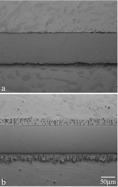
Typical micrographs of OM for the cross-sections of the annealed diffusion couples are shown in Fig. 1. The (Sn– 5Au)/Ni/(Sn–5Au) diffusion couple is hereafter merely called the Sn–5Au diffusion couple. Figure 1(a) indicates the micrograph for the Sn–5Au diffusion couple with T ¼ 433K andt¼12h (4:32105s). In this figure, the regions on the upper and lower sides are the Sn–5Au alloy, and the horizontal band with a thickness of about 100mmis the Ni specimen. As can be seen, sound interconnection is realized at the interface between the Sn–5Au alloy and the Ni specimen. However, no compound layer is clearly observed at the interface. As a result, annealing was carried out for much longer periods at T¼433K. On the other hand, Fig. 1(b) shows the micrograph for the Sn–5Au diffusion couple withT ¼473K and t¼48h (1:73105s). In this
case, a layer composed of various compounds with different contrasts is formed along each interface. Such a layer grows mainly towards the Sn–5Au alloy but slightly towards the Ni specimen. The microstructure in Fig. 1(b) is magnified in Fig. 2(a). This figure indicates a micrograph of BEI. In Fig. 2(a), the regions on the upper and lower sides are the Sn–
5Au alloy and the Ni specimen, respectively. As to the Sn– 5Au alloy, coarse bright grains are distributed in a dark matrix. The chemical composition of each phase was measured by EPMA. According to the EPMA measurement, the bright grain and the dark matrix are AuSn4 and the
primary solid-solution phase of Sn, respectively. A phase diagram in the binary Au–Sn system31)indicates that the Sn phase is in equilibrium with AuSn4 atT <490K.
Further-more, the solubility of Au in the Sn phase is less than 0.2 at%.31)Thus, the SnþAuSn4two-phase microstructure is
stable for the Sn–5Au alloy atT¼433{473K. In contrast, a layer consisting of bright and dark compounds is produced along the (Sn–Au)/Ni interface as mentioned earlier. The EPMA measurement shows that the bright and dark com-pounds are AuNiSn8 and Ni3Sn4, respectively. As can be
seen in Fig. 2(a), Ni3Sn4 is formed as a slightly wavy thin
layer along the interface between the AuNiSn8layer and the
Ni specimen, and dispersed as fine particles in the AuNiSn8
layer. The thickness is much smaller for the Ni3Sn4layer than
for the AuNiSn8 layer. This means that interdiffusion takes
place much faster across the AuNiSn8 layer than across the
Ni3Sn4layer.32)The same type of microstructure as Fig. 2(a)
was observed for most of the annealed diffusion couples. On the other hand, Fig. 2(b) indicates the BEI micrograph for the Sn–5Au diffusion couple withT ¼473K andt¼722h
(2:60106s). As can be seen, the AuNiSn
8 and Ni3Sn4
layers are produced also in this diffusion couple. In Fig. 2(b), however, voids with a dark contrast are recognized along the interface between the AuNiSn8 layer and the Sn–5Au alloy.
Such voids are considered to form due to the Kirkendall effect. The occurrence of the Kirkendall effect indicates that the interdiffusion occurs according to a vacancy mechanism. The formation of voids was clearly observed only for the diffusion couples with T ¼473K and t¼722 and 840 h (2:60106and3:02106s).
Recently, a phase diagram in the ternary Au–Ni–Sn system was experimentally determined by Liuet al.33)According to their result, a three-phase equilibrium of SnþAuSn4þ
Ni3Sn4as well as two-phase equilibria of SnþAuSn4, Snþ
Ni3Sn4and AuSn4þNi3Sn4appears at the Sn-rich corner of
the isothermal section with T¼473K. The solubility of Ni in AuSn4 is 11.5 at% at T ¼473K.33) This yields the
composition Au0:85Ni1:15Sn8. The composition AuNiSn8 is
close to Au0:85Ni1:15Sn8. Consequently, the microstructure
for the compound layers in the Sn–5Au diffusion couple is well explained by the phase equilibria in the ternary Au–Ni– Sn system.
3.2 Growth behavior of intermetallic layer
From the cross-sectional BEI micrographs like Fig. 2, the total thicknesslof the compound layers was evaluated by the equation
Fig. 1 Optical micrographs of cross-sections for the Sn–5Au diffusion couples annealed (a) atT¼433K fort¼12h (4:32104s) and (b) at
T¼473K fort¼48h (1:73105s).
Fig. 2 Back-scattered electron images of cross-sections for the Sn–5Au diffusion couples annealed atT¼473K for (a)t¼48h (1:73105s)
[image:3.595.315.542.70.407.2] [image:3.595.57.283.73.431.2]l¼A=w; ð1Þ
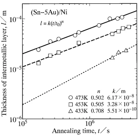
whereAandware the total area and the total length of the compound layers, respectively, on the cross-section. Here-after, the layer composed of various compounds is called the intermetallic layer. At each annealing time,lwas calculated from eq. (1) using the total values of A and wfor various cross-sections. The results of T ¼433, 453 and 473 K are shown as open triangles, squares and circles, respectively, in Fig. 3. In this figure, the ordinate indicates the logarithm of the thicknessl, and the abscissa shows the logarithm of the annealing time t. As can be seen, the thickness l mono-tonically increases with increasing annealing time t. The plotted points at each annealing temperature lie well on a straight line. This deduces that l is expressed as a power function oftby the following equation:
l¼kðt=t0Þn: ð2Þ
Here,t0is unit time, 1 s. It is adopted to make the argument
t=t0of the power function dimensionless. The proportionality
coefficientkhas the same dimension as the thickness l, but the exponent nis dimensionless. From the plotted points in Fig. 3, the values of k and n were evaluated by the least-squares method. The evaluated values are indicated in Fig. 3. Using these values ofkandn, the thicknesslwas calculated as a function of the annealing timetfrom eq. (2). The results ofT ¼433, 453 and 473 K are shown as dotted, dashed and solid lines, respectively, in Fig. 3. At each annealing time, the thicknessl increases with increasing annealing temper-ature T. Thus, the higher the annealing temperature is, the larger the overall growth rate of the intermetallic layer becomes. As mentioned in Section 3.1, the Kirkendall voids are formed along the interface between the AuNiSn8 layer
and the Sn–5Au alloy at T ¼473K fort¼722 and 840 h (2:60106and3:02106s). However, the two open circles for these annealing times are located well on the solid line of
T ¼473K in Fig. 3. Thus, it is concluded that formation of the Kirkendall voids hardly affects the growth rate of the intermetallic layer.
The results of T¼453 and 473 K in Fig. 3 are plotted again as open circles with solid lines in Figs. 4(a) and (b), respectively. As mentioned in Section 1, the reactive diffusion was experimentally observed at solid-state temper-atures for the binary Sn/Ni17)and Sn/Au18–20)systems using
the Sn/Ni/Sn and Sn/Au/Sn diffusion couples, respectively, in previous studies. The Sn/Au/Sn and Sn/Ni/Sn diffusion couples are denoted by the Au and Ni diffusion couples, respectively. The intermetallic layer consisting of AuSn4,
AuSn2 and AuSn is formed at T¼393{473K in the Au
diffusion couple, but that composed of only Ni3Sn4 is
[image:4.595.55.285.68.293.2]produced atT ¼453{473K in the Ni diffusion couple. The experimental values oflfor the Au and Ni diffusion couples are represented as open squares and triangles, respectively, in Fig. 4. From these open symbols, k andn in eq. (2) were evaluated by the least-squares method. The evaluated values are shown in Fig. 4. Using these values of k andn,l was calculated as a function oftfrom eq. (2). The results for the Au and Ni diffusion couples are indicated as dashed and dotted lines, respectively, in Fig. 4. At each annealing temperature and time, the thickness lis about one order of magnitude greater for the Sn–5Au diffusion couple than for the Ni diffusion couple, but smaller for the Sn–5Au diffusion couple than for the Au diffusion couple. In the Sn–5Au diffusion couple, the intermetallic layer consisting of AuNiSn8 and Ni3Sn4 is produced by the reactive diffusion
between Ni and SnþAuSn4. The overall growth rate of the
intermetallic layer is greater for the reactive diffusion between Ni and SnþAuSn4 than for that between Ni and
Sn but smaller for that between Ni and SnþAuSn4than for
that between Au and Sn. Thus, the Ni layer still works as an inhibitor against the reactive diffusion between the Au/Ni/ Cu multilayer conductor and Sn-base solder alloys during energization heating, even if AuSn4is non-uniformly formed
in the molten solder and the Au layer of the Au/Ni/Cu multilayer conductor alloy is completely depleted during soldering.
3.3 Rate-controlling process
The values of the exponentn for the Sn–5Au, Au and Ni diffusion couples are plotted against the annealing temper-atureTas open circles, squares and triangles, respectively, in Fig. 5. Here, the ordinate and the abscissa indicatenandT, respectively. The reactive diffusion in the ternary Sn/(Au– Ni) system was experimentally observed using Sn/(Au– 27Ni)/Sn and Sn/(Au–46Ni)/Sn diffusion couples in a previous study.29) The Sn/(Au–27Ni)/Sn and Sn/(Au–
46Ni)/Sn diffusion couples are merely called the Au–27Ni and Au–46Ni diffusion couples, respectively. During iso-thermal annealing atT ¼433{473K, the intermetallic layer composed of Au1:5Ni0:5Sn8 and AuNi2Sn4 is formed along
the Sn/(Au–Ni) interface in the Au–46Ni diffusion couple, but that consisting of Au1:7Ni0:3Sn8, AuSn2 and Au6Ni4Sn15
dispersed with fine particles of AuNi2Sn4 is produced along
the interface in the Au–27Ni diffusion couple. Also for these diffusion couples, the total thickness l of the intermetallic layer is expressed as a power function of the annealing timet Fig. 3 The total thicknesslof the intermetallic layer versus the annealing
timetfor the Sn–5Au diffusion couple atT¼433, 453 and 473 K shown as open triangles, squares and circles, respectively. Straight lines indicate the calculations from eq. (2).
by eq. (2). The values of the exponentnfor the Au–27Ni and Au–46Ni diffusion couples29) are represented as open
rhombuses and inverse-triangles, respectively, in Fig. 5. As to the Au diffusion couple, n is equal to 0.36 at
T ¼473K, and monotonically increases with decreasing annealing temperature.18–20)AtT ¼393K,nis close to 0.5.
When the volume diffusion of the constituent elements in each phase is the rate-controlling process for the growth of the intermetallic layer,nis equal to 0.5. On the other hand, the growth will be governed by the grain boundary diffusion along grain boundaries with a finite thickness in the intermetallic layer at low annealing temperatures where the volume diffusion is practically frozen out. If grain growth takes place in the intermetallic layer, the volume fraction of the grain boundaries monotonically decreases with increas-ing annealincreas-ing time. Such decrease in the volume fraction
results in the decrement of the effective cross-section, and decelerates the grain boundary diffusion. Thus, n becomes smaller than 0.5. When the grain size is proportional to the square root of the annealing time,nis equal to 0.25.34)If the grain growth occurs very sluggishly, the volume fraction of the grain boundaries remains almost constant during anneal-ing. In such a case, the effective cross-section for the grain boundary diffusion hardly varies, and hencenis almost equal to 0.5. From the temperature dependence of n for the Au diffusion couple in Fig. 5, it is concluded that the grain boundary diffusion as well as the volume diffusion contrib-utes to the rate-controlling process and the grain growth takes place at certain rates at higher annealing temperatures.19,20)
As the annealing temperature decreases, the contribution of the grain boundary diffusion becomes remarkable, but the grain growth slows down. Similar temperature dependence of the rate-controlling process was recognized also for the Ni17) and Au–27Ni29)diffusion couples.
On the other hand, for the Sn–5Au diffusion couple,n is close to 0.5 atT ¼453{473K, but equal to 0.7 atT ¼433K. Like the Au, Ni and Au–27Ni diffusion couples, the grain growth in the intermetallic layer may occur at certain rates also for the Sn–5Au diffusion couple. Nevertheless,nis close to 0.5 at T ¼453{473K for the Sn–5Au diffusion couple. This means that the volume diffusion is the rate-controlling process.25)AtT ¼433K, however,nis equal to 0.7 for the
Sn–5Au diffusion couple. Thus, interface reaction contrib-utes to the rate-controlling process.27,30)According to the OM
micrographs in Fig. 1, the intermetallic layer grows mainly towards the Sn–Au alloy but slightly towards the Ni specimen. Furthermore, the most predominant compound determining the overall growth rate of the intermetallic layer is AuNiSn8. Therefore, the growth rate of the intermetallic
layer is dominantly determined by the migration rate of the AuNiSn8/(Sn–Au) interface. As a consequence, for the Sn– Fig. 4 The results ofT¼453and 473 K in Fig. 3 are represented as open
circles with solid lines in (a) and (b), respectively. The results for the Ni17) and Au19,20) diffusion couples are also shown as open triangles and squares, respectively.
[image:5.595.54.285.68.520.2] [image:5.595.311.542.72.297.2]5Au diffusion couple, the interface reaction at the migrating AuNiSn8/(Sn–Au) interface becomes the bottleneck for the
growth of the intermetallic layer at T¼433K. The same temperature dependence of the rate-controlling process as the Sn–5Au diffusion couple was observed for the Au–46Ni diffusion couple.29)
This type of rate-controlling process was experimentally examined for the reactive diffusion in the ternary (Cu–Sn)/ Nb system in a previous study.27)In that experiment, (Cu–
Sn)/Nb/(Cu–Sn) diffusion couples with a concentration of 8.3 at% Sn were isothermally annealed at temperatures of
T ¼923{1053K. During annealing, a layer of Nb3Sn is
formed along the (Cu–Sn)/Nb interface in the diffusion couple, and the thickness lof the Nb3Sn layer increases in
proportion to a power function of the annealing timet. Thus, the growth of the Nb3Sn layer is also described by eq. (2).
Since the Nb3Sn layer grows mainly towards the Nb
specimen, the migration of the Nb3Sn/Nb interface
princi-pally governs the growth of the Nb3Sn layer. The exponentn
in eq. (2) is nearly equal to unity at T ¼923{973K and monotonically decreases from 1 to 0.8 with increasing annealing temperature fromT¼973K toT ¼1053K. This indicates that the interface reaction at the Nb3Sn/Nb
inter-face is the rate-controlling process for the growth of the Nb3Sn layer at T ¼923{973K and the volume diffusion
across the Nb3Sn layer contributes to the rate-controlling
process at T¼973{1053K. In the temperature range of
T ¼923{973K, the temperature dependence of the propor-tionality coefficientkin eq. (2) was expressed as
k¼k0expðQk=RTÞ; ð3Þ
and then the activation enthalpy Qk was evaluated to be
150 kJ/mol.27)Here,k
0 andRare the pre-exponential factor
and the gas constant, respectively. The value Qk¼150
kJ/mol represents the activation enthalpy of the interface reaction at the Nb3Sn/Nb interface. On the other hand, the
corresponding value ofQkfor the rate-controlling process of
the volume diffusion was estimated as 100 kJ/mol.27) The
smaller the value ofQkis, the less sensitive the temperature
dependence of k becomes. As the annealing temperature increases, the rate of the interface reaction increases more remarkably than that of the volume diffusion. Therefore, the interface reaction is no longer the bottleneck for the migration of the Nb3Sn/Nb interface at higher annealing
temperatures. This is the reason why the interface reaction is the rate-controlling process at T ¼923{973K but the volume diffusion contributes to the rate-controlling process at T¼973{1053K. Such an explanation may be possible also for the temperature dependence of the rate-controlling process for the Sn–5Au and Au–46Ni diffusion couples. Unfortunately, however, the value ofQkis not known for the
interface reaction in these diffusion couples. Consequently, the explanation is not available for the Sn–5Au and Au–46Ni diffusion couples, though the activation enthalpy of the volume diffusion has been estimated below.
When the reactive diffusion is controlled by the volume diffusion, the growth of the intermetallic layer is expressed by the following equation:32)
l2¼Kt: ð4Þ
Equation (4) is a formula of the parabolic relationship, where
K is the parabolic coefficient with a dimension of m2/s. As mentioned above, the volume diffusion is the rate-controlling process for the Sn–5Au diffusion couple atT ¼453{473K. Thus, the values ofKatT ¼453and 473 K for the Sn–5Au diffusion couple were evaluated from eq. (4) using the open squares and circles, respectively, in Fig. 3 by the least-squares method. The evaluation givesK¼1:231014and 4:031014m2/s at T ¼453 and 473 K, respectively.
These values are plotted against the annealing temperature
T as open circles in Fig. 6. In this figure, the ordinate shows the logarithm ofK, and the abscissa indicates the reciprocal of T. The temperature dependence ofK is described by the following equation with certain accuracy:35–38)
K¼K0expðQK=RTÞ: ð5Þ
Here, K0 and QK are the pre-exponential factor and the
activation enthalpy, respectively. Interconnecting the two open circles with a solid line in Fig. 6, we obtain K0¼ 1:92103m2/s and QK ¼106kJ/mol for the Sn–5Au
diffusion couple. As mentioned earlier, the growth of the intermetallic layer is controlled by the volume diffusion also for the Au–46Ni diffusion couple at T ¼453{473K. The values of K for the Au–46Ni diffusion couple29) are
represented as open squares in Fig. 6. Interconnection of the two open squares with a dashed line yieldsK0¼2:26 105m2/s andQ
K¼79:3kJ/mol.29)
The reactive diffusion in the binary Sn/Pd system was experimentally observed atT ¼433{473K using Sn/Pd/Sn diffusion couples in a previous study.25) The Sn/Pd/Sn diffusion couple is denominated the Pd diffusion couple. For the Pd diffusion couple, the intermetallic layer is composed of PdSn4, PdSn3and PdSn2atT ¼433K but only PdSn4and
PdSn3 at T¼453 and 473 K. Although the grain growth
surely occurs in the intermetallic layer, the thickness l is
Fig. 6 The parabolic coefficientKversus the reciprocal of the annealing temperatureTfor the Sn–5Au diffusion couple shown as open circles. The results for the Pd,25) Cu39) and Au–46Ni29) diffusion couples are also indicated as open triangles, rhombuses and squares, respectively. Straight lines show the calculations from eq. (5).
[image:6.595.312.543.71.287.2]almost proportional to the square root of the annealing timet
atT¼433{473K.25)This guarantees that the growth of the
intermetallic layer is governed by the volume diffusion. The values of K for the Pd diffusion couple are represented as open triangles in Fig. 6. From the open triangles, K0¼ 8:20102m2/s andQ
K ¼106kJ/mol are obtained by the
least-squares method. In contrast, Onishi and Fujibuchi experimentally observed the reactive diffusion in the binary Sn/Cu system at T¼463{493K using Sn/Cu diffusion couples.39)The Sn/Cu diffusion couple is denoted by the Cu
diffusion couple. The values ofKfor the Cu diffusion couple are also represented as open rhombuses in Fig. 6. For the open rhombuses, K0¼6:231010m2/s and QK ¼57:7
kJ/mol were reported by Onishi and Fujibuchi.39)Using these values of K0 andQK, K was calculated as a function of T
from eq. (5). The results for the Pd and Cu diffusion couples are indicated as dotted and dashed-and-dotted lines, respec-tively, in Fig. 6. As can be seen,Kis smaller for the Sn–5Au diffusion couple than for the Au–46Ni and Pd diffusion couples, but greater for the Sn–5Au diffusion couple than for the Cu diffusion couple. The overall growth rate of the intermetallic layer is close to each other for the Pd and Au diffusion couples.19,20,25)Thus, the reactive diffusion between
Ni and SnþAuSn4occurs more slowly than that between Au
and Sn but more rapidly than that between Cu and Sn. Consequently, Ni layer still acts as an inhibitor against the reactive diffusion between the Au/Ni/Cu multilayer con-ductor and Sn-base solder alloys during energization heating, even if AuSn4is formed in the molten solder and the Au layer
is completely depleted during soldering. However, the kinetics of this reactive diffusion is faster than that of the reactive diffusion between the Cu-base conductor and Sn-base solder alloys. The valueQK ¼106kJ/mol for the Sn–
5Au and Pd diffusion couples is rather close to that QK¼ 79:3kJ/mol for the Au–46Ni diffusion couple, but greater than that QK ¼57:7kJ/mol for the Cu diffusion couple.
When the intermetallic layer consists of compound layers with parallel interfaces and temperature dependencies of interdiffusion coefficients in relevant phases are known for reactive diffusion in a binary system, QK is quantitatively
related with the activation enthalpiesQof the interdiffusion coefficients in an analytical manner.35–37)Even in such a case, however, complex information ofQfor the relevant phases is included inQK. Hence, it may not be valid to discuss the
rate-controlling process of the reactive diffusion only from the value ofQK.
4. Conclusions
The reactive diffusion in the ternary (Sn–Au)/Ni system was experimentally observed at solid-state temperatures using the sandwich (Sn–5Au)/Ni/(Sn–5Au) diffusion couple prepared by the diffusion bonding technique. The diffusion couple was isothermally annealed in the temperature range betweenT¼433and 473 K for various times up to 1057 h in the oil bath with silicone oil. In this temperature range, the coarse grains of AuSn4 are distributed in the primary
solid-solution phase of Sn for the binary Sn–5Au alloy. During annealing, the AuNiSn8and Ni3Sn4layers are formed along
the (Sn–Au)/Ni interface in the diffusion couple. The total
thicknesslof the compound layers is expressed as a power function of the annealing timetby the equationl¼kðt=t0Þn,
where t0 is unit time, 1 s. Here, n is close to 0.5 at T ¼ 453{473K, but equal to 0.7 at T¼433K. This means that the growth of the compound layers is controlled by the volume diffusion of the constituent elements in each phase at
T ¼453{473K but the interface reaction at the migrating AuNiSn8/(Sn–Au) interface contributes to the
rate-control-ling process at T ¼433K. The overall growth rate of the compound layers is smaller for the ternary (Sn–Au)/Ni system than for the binary Sn/Au system, but greater for the ternary (Sn–Au)/Ni system than for the binary Sn/Ni and Sn/Cu systems.
Acknowledgements
The authors are grateful to Messrs. K. Sakamoto and N. Kurokawa at Tyco Electronics AMP Co. Ltd., Japan for stimulating discussions. They also wish to thank Professor K. Ishida and Professor R. Kainuma at Tokohu University, Japan for their helpful information of the phase equilibria in the ternary Au–Ni–Sn system. The present study was supported by Tyco Electronics AMP Co. Ltd., Japan. The study was also partially supported by a Grant-in-Aid for Scientific Research from the Ministry of Education, Culture, Sports, Science and Technology of Japan.
REFERENCES
1) L. Zakraysek: Welding Res. Suppl. Nov. (1972) 536–541. 2) K. N. Tu: Acta Metall.21(1973) 347–354.
3) H. N. Keller: IEEE Trans. Components Hybrids Manuf. Tech. CHMT-2 (1979) 180–195.
4) H. N. Keller and J. M. Morabito: Surf. Interface Anal.3(1981) 16–22. 5) J. O. G. Parent, D. D. L. Chung and I. M. Bernstein: J. Mater. Sci.23
(1988) 2564–2572.
6) A. J. Sunwoo, J. W. Morris, Jr. and G. K. Lucey, Jr.: Metall. Trans. A 23(1992) 1323–1332.
7) P. T. Vianco, P. F. Hlava and A. L. Kilgo: J. Electron. Mater.23(1994) 583–594.
8) D. R. Frear and P. T. Vianco: Metall. Trans.25A(1994) 1509–1523. 9) S. Choi, T. R. Bieler, J. P. Lucas and K. N. Subramanian: J. Electron.
Mater.28(1999) 1209–1215.
10) P. G. Kim and K. N. Tu: J. Appl. Phys.80(1996) 3822–3827. 11) A. M. Minor and J. W. Morris, Jr.: Metall. Mater. Trans.31A(2000)
798–800.
12) J. H. Lee, J. H. Park, Y. H. Lee and Y. S. Kim: J. Mater. Res.16(2001) 1249–1251.
13) H. G. Song, J. P. Ahn, A. M. Minor and J. W. Morris, Jr.: J. Electron. Mater.30(2001) 409–414.
14) M. O. Alam and Y. C. Chan: Chem. Mater.15(2003) 4340–4342. 15) M. O. Alam and Y. C. Chan: J. Mater. Res.19(2004) 1303–1306. 16) C. M. Chen and S. W. Chen: Acta Mater.50(2002) 2461–2469. 17) M. Mita, M. Kajihara, N. Kurokawa and K. Sakamoto: Mater. Sci. Eng.
A403(2005) 269–275.
18) M. Kajihara, T. Yamada, K. Miura, N. Kurokawa and K. Sakamoto: Netsushori43(2003) 297–298.
19) T. Yamada, K. Miura, M. Kajihara, N. Kurokawa and K. Sakamoto: J. Mater. Sci.39(2004) 2327–2334.
20) T. Yamada, K. Miura, M. Kajihara, N. Kurokawa and K. Sakamoto: Mater. Sci. Eng. A390(2005) 118–126.
21) T. Takenaka, S. Kano, M. Kajihara, N. Kurokawa and K. Sakamoto: Mater. Sci. Eng. A396(2005) 115–123.
22) M. Mita, K. Miura, T. Takenaka, M. Kajihara, N. Kurokawa and K. Sakamoto: Mater. Sci. Eng. B126(2006) 37–43.
Mater. Trans.46(2005) 1825–1832.
24) K. Suzuki, S. Kano, M. Kajihara, N. Kurokawa and K. Sakamoto: Mater. Trans.46(2005) 969–973.
25) T. Takenaka, M. Kajihara, N. Kurokawa and K. Sakamoto: Mater. Sci. Eng. A406(2005) 134–141.
26) T. Takenaka and M. Kajihara: Mater. Trans.47(2006) 822–828. 27) Y. Muranishi and M. Kajihara: Mater. Sci. Eng. A404(2005) 33–41. 28) T. Takenaka, M. Kajihara, N. Kurokawa and K. Sakamoto: Mater. Sci.
Eng. A427(2006) 210–222.
29) Y. Yato and M. Kajihara: Mater. Sci. Eng. A428(2006) 276–283. 30) T. Hayase and M. Kajihara: Mater. Sci. Eng. A, in press.
31) T. B. Massalski, H. Okamoto, P. R. Subramanian and L. Kacprzak:
Binary Alloy Phase Diagrams(ASM International, Materials Park, OH, 1990) vol. 1, p. 434.
32) M. Kajihara: Acta Mater.52(2004) 1193–1200.
33) X. J. Liu, M. Kinaka, Y. Takaku, I. Ohnuma, R. Kainuma and K. Ishida: J. Electron. Mater.34(2005) 670–679.
34) Y. L. Corcoran, A. H. King, N. de Lanerolle and B. Kim: J. Electron. Mater.19(1990) 1177–1183.
35) M. Kajihara: Mater. Sci. Eng. A403(2005) 234–240. 36) M. Kajihara: Mater. Trans.46(2005) 2142–2149. 37) M. Kajihara: Def. Diff. Forum249(2006) 91–96. 38) M. Kajihara: Mater. Trans.47(2006) 1480–1484.
39) M. Onishi and H. Fujibuchi: Trans. JIM16(1975) 539–547.