Al-doped ZnO thin films were prepared on the (0001) sapphire (c-Al2O3) substrates by atomic layer deposition (ALD) using alternating pulses of Zn(C2H5)2, Al(CH3)3and H2O precursors and post-deposition high-temperature annealing. Photoluminescence (PL) spectroscopy showed that the threshold of stimulated emission decreases with increasing Al concentration, from 49.2 kW/cm2of the ZnO film to 12.2 kW/ cm2of the ZnO film nominally containing 4% Al. This reduction is attributable to the increase in the optical scattering resulting from segregation of excess Al in heavily Al-doped ZnO films. The structure of these films was investigated by analytical scanning-transmission electron microscopy (STEM) as well as X-ray diffraction (XRD). It was revealed that a single crystal ZnO layer containing a small amount of Al is formed with the orientation relation with respect to thec-Al2O3: [0001]ZnO==[0001]Al2O3 and [01110]ZnO==[211110]Al2O3, and that a polycrystalline ZnAl2O4layer is formed between the ZnO layer and thec-Al2O3substrate. The electron microscopy observation accounts for the results of the electro-optical experiments. The growth mechanism of the observed two layers is discussed.
[doi:10.2320/matertrans.MC200902]
(Received July 29, 2009; Accepted October 15, 2009; Published December 2, 2009)
Keywords: atomic layer deposition, ultra-violet light emission diode, zinc-oxide, X-ray diffraction, photoluminescence spectroscopy, analytical scanning-transmission electron microscopy
1. Introduction
Zinc oxide is one of promising materials for ultraviolet (UV) photonic devices because of the high direct band-gap energy of 3.37 eV at room temperature and the large exciton binding energy up to 60 meV, exhibiting various chemical,
environmental and economical advantages.1–13) Many
tech-niques have been utilized for growing high-quality ZnO
films, such as molecular beam epitaxy,1–3) metal-organic
chemical vapor deposition,4,5) hybrid beam deposition,6)
chemical vapor deposition7,8) and pulsed laser deposition
(PLD).9,10) Another prospective method for preparing ZnO
films is atomic layer deposition (ALD).11–13) ALD is a
surface-controlled process for depositing materials with atomic-layer accuracy. One of the presenting authors and his colleagues prepared high-quality ZnO thin films on the
(0001)-sapphire (c-Al2O3) substrates by ALD, and observed
stimulated emission from the ZnO films.14) They have also
fabricated light-emitting diodes (LEDs) composed ofn-ZnO/
p-GaN heterojunction,15) n-ZnO:Al/SiO
2-ZnO
nanocompo-site/p-GaN:Mg16,17)andn-ZnO/ZnO nanodots-SiO
2
compo-site/p-AlGaN by ALD,18)all of which emitted significant UV
electroluminescence from the n-ZnO layers. In addition to
the application in UV photonic devices, ZnO is also known as a transparent conductive oxide. The doping of ZnO with group-III impurities such as Al improves electrical
conduc-tivity. Recently, Wang et al.,19) who investigated undoped
ZnO thin films grown on thec-Al2O3substrate at 600C by
PLD, have reported an increase in electron concentration and lowering of the threshold of optical-pumped stimulated
emission from ZnO by thermal annealing (900C, 2 h). They
attributed this phenomenon to diffusion of Al from Al2O3
into ZnO, assuming the formation of a ZnAl2O4 crystalline
layer at the ZnO/Al2O3 interface.
In our work, we employed an ALD technique followed by high-temperature annealing to prepare heavily Al-doped ZnO (ZnO:Al) films. The electrical and optical properties, as well as the structure of the prepared films were investigated to elucidate the effect and behavior of Al doping.
2. Experiment
Heavily Al-doped ZnO thin films were deposited on the
c-Al2O3substrate at a temperature as low as 180C by ALD
using alternating pulses of Zn(C2H5)2 (Diethylzinc, DEZn),
Al(CH3)3(Trimethylaluminum, TMA) and H2O vapor in an
N2carrier gas flow. The ALD process consisted of two kinds
of cycles; cycle I contained the following sequence: DEZn,
0:01s!N2 purge, 5s!H2O, 0:1s!N2 purge, 5 s for
the growth of ZnO, and cycle II contained TMA,
0:03s!N2 purge, 5s!H2O, 0:1s!N2 purge, 5 s for
the doping of Al. The total number of the ALD cycles was 1500, where one cycle of II was performed every 49 cycles of I to prepare nominal ZnO:Al (2%) film, as shown in Fig. 1. To prepare nominal ZnO:Al (4%) film, one cycle of II was performed every 24 cycles of I. After deposition, the films
were annealed at 1000C for 2 h in N
2 atmosphere to
homogenize the composites and improve the crystallinity. The post-annealed ZnO:Al films were analyzed by means of photoluminescence (PL), Hall effect measurement with the van der Pauw configuration, X-ray diffraction (XRD) and analytical scanning-transmission electron microscopy (STEM). The room temperature PL spectra of the ZnO:Al *1Graduate Student, National Taiwan University
films were measured using a fourth harmonic Q-switched Nd:YAG laser (266 nm, 10 ns, 15 Hz) as the excitation source, in the standard backscattering configuration. For analytical STEM observation, the specimens with a low-index zone axis were embedded into Ti rings, ground, dimpled, and ion-milled in two steps: until perforation they were ion-milled at 4 keV, beam current of 1.0 mA, incident
angle of 10 (Bal-Tec RES010) and additionally ion-milled
at low-energy on both sides under oscillation at 300 eV
(Technoorg Linda, model IV5).20)The additional low-energy
ion-milling significantly reduced the amorphous layer and artifacts caused by the sputtering. STEM, high-resolution transmission electron microscopy (HRTEM) and energy dispersive X-ray spectroscopy (EDXS) were performed in a JEM-2010F TEM/STEM, operated at 200 keV, equipped
with a pole piece ofCS¼0:48mm.
3. Results and Discussion
Before structural investigation, we examined the electro-optical properties of the prepared specimens. PL spectra from the ZnO film and ZnO:Al (4%) film are shown in Figs. 2(a) and 2(b), respectively. The spontaneous emission, which is
associated with the free excitons or bond excitons,21,22)was
observed at 383 nm with a low excitation intensity. Increase in excitation intensity causes the exciton concentration to reach the Mott density, where the excitons overlap with each other, lose their individual character and become electron-hole plasma (EHP). Hence, spectral peaks attributed to EHP appear around 394 nm at high excitation intensities. With further increase in the excitation intensity, the EHP peaks gradually dominate the emission spectrum and shift toward lower energy due to the band-gap renormalization, which are
similar to the behavior previously reported.23–25) The insets
show the plots of the integrated PL intensity versus the
excitation intensity. The integrated PL intensity increases rapidly as the excitation intensity is greater than a threshold value. The appearance of the spectral peaks, as well as significant increase in the emission intensity after the threshold indicate that the stimulated emission takes place in the ZnO:Al film. The thresholds for stimulated emission
of the ZnO film and the ZnO:Al (4%) film are 49.2 kW/cm2
and 12.2 kW/cm2, respectively. Since the diameter of the
incident laser beam used in this study was about 1 mm, which is much larger than the film thickness, it is likely that the stimulated emission was caused by the closed-loop paths in
the direction parallel to the film surface via multiple
scattering between optical scattering centers and crystalline grains. The scattering of the stimulated emission propagating in the in-plane direction might lead to the observed stimulated emission in the direction perpendicular to the film surface.
Table 1 summarizes electrical properties of the ZnO:Al films characterized by the Hall effect measurement, together with the threshold for stimulated emission. All samples
exhibited n-type conductivity. The electron concentrations
are of the same order of magnitude (1018cm3) and only
slightly decrease with increasing Al content, suggesting that Al concentration is almost the same among the samples and that a large amount of Al atoms may segregate in heavily doped ZnO:Al films due to the solid solubility limit of Al in ZnO. The solid solubility limit was estimated to be 2 mol%
from XRD and Raman spectroscopy by Yoo et al.26) The
segregation of Al might cause optical scattering centers in the ZnO:Al films. The increase in optical scattering centers due to Al doping may facilitate the formation of closed-loop paths for light through multiple optical scattering, leading to
the decrease in the threshold of stimulated emission.27,28)
Additionally, it is clearly seen from Fig. 2(b) that there are
Fig. 1 Atomic layer deposition (ALD) of heavily Al-doped ZnO thin films. The ALD for the ZnO:Al (2%) film is indicated.
[image:2.595.76.266.67.220.2] [image:2.595.311.542.71.404.2]many narrow spectral peaks appearing upon the emission spectra of the ZnO:Al (4%) film. On the other hand, the undoped ZnO exhibits relatively smooth emission spectra (Fig. 2(a)). The appearance of the narrow spectral peaks upon the spectra of the ZnO:Al (4%) may be attributed to the constructive closed-loop paths due to optical scattering provided by the Al segregation in the heavily doped ZnO:Al films.29)In the Table 1 the data reported by Wanget al.19)are also included. It is not obvious why ZnO layer prepared by Wang et al. had a higher carrier concentration of 1:6
1019cm3as compared to our samples, while it had the same
order of the threshold with the present samples.
In order to explain the above-mentioned electro-optical and electrical results, XRD and HRTEM/STEM investiga-tions were performed. Figure 3(a) shows XRD patterns of the post-annealed ZnO:Al films. The appearance of strong ZnO (0002) peaks reveals the preferential (0002)-orientation of
the ZnO:Al films in respect with c-Al2O3 crystal of the
substrate. The full-width at half-maximum (FWHM) of the
ZnO (0002) K1 peaks is shown in Fig. 3(b). The
crystal-linity becomes worse with increasing Al concentration that is
from 0.08 to 0.12. Incidentally, the FWHM for the (0002)
reflection of the ZnO sample of Wanget al., grown on thec
-Al2O3substrate at 600C by PLD and post annealed at 900C
for 2 h, was 0.15.19)The FWHM of our X-ray measurements
was obtained from the line profile of -2 scanning which
was recorded along the reciprocal vectorgin the reciprocal
space, while their FWHM was of the !-scanning rocking
curve which was recorded along the direction perpendicular to both, the reciprocal vector and the incident X-ray wave vector. Although the scanning manner is different between the two measurements, Fig. 3(b) seems to confirm the good quality of these ZnO crystals. The broadening of the ZnO (0002) peak might result from the distortion of ZnO crystal lattice due to heavy doping of Al. Since the solid solubility
limit of Al in ZnO is only 2 mole%,26)a large amount of Al
atoms might segregate from the surrounding ZnO, leading to the dramatic broadening of ZnO (0002) peak in the ZnO:Al (4%).
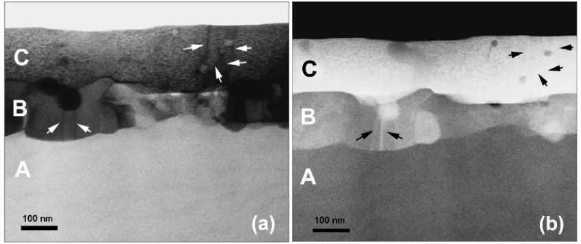
Figures 4(a) and 4(b) show bright-field (BF) and high-angle dark-field (HAADF) STEM images of the ZnO:Al (2%), respectively. We can clearly distinguish three different
layers, namely,A,BandC. Figure 5 shows BF-STEM image
from an area in the ZnO:Al (2%) with overall EDXS spectrum and the corresponding X-ray mappings using characteristic X-rays emitted from Al, Zn, and O and C. The carbon signal originates from adhesive that was used for STEM specimen preparation and which was deposited on the
Fig. 3 (a) X-ray diffraction patterns and (b) FWHM of the (0002) peaks of the ZnO, ZnO:Al (2%), and ZnO:Al (4%) films.
[image:3.595.303.547.73.230.2] [image:3.595.46.290.95.191.2] [image:3.595.86.509.283.461.2]specimen surface during the ion-milling, in spite of careful
specimen preparation.20)The mappings reveal that the layer
A, characterized only with Al and O emission, is the Al2O3
layer, the layer B is composed of Zn, Al and O, while the
layerCis a ZnO layer. This was additionally confirmed by
semi-quantitative EDXS analysis shown in Fig. 6. The probe
size that was used for the EDX spectroscopy was 0:5nm.
However, all the EDX spectra were acquired from frames and not from points (spot mode) in order to obtain an average
composition from a relatively larger area.29) The
beam-broadening effect in this case did not affect the peak intensities and/or the ratios in the EDXS spectra. The EDXS
analysis was performed from an area of 1010nm2,
indicated by regions p1p4. The spectra sp1, sp2, sp3 and
sp4 were acquired from the area p1 in layerA, p2 in layerB,
and p3 and p4 in layerC, respectively. The spectra sp3 and
sp4 reveal that the ZnO in layer Ccontains a small amount
of Al atoms.
Figure 7 shows an HRTEM image of an area including
layerBand layerC. Fourier transformation (FT) images from
the inset squares are also presented. The FT image from the
layer C (lower part) reveals that the corresponding image
comprises the (0002) and (11220) lattice fringes of the ZnO
crystal with the wurtzite structure. Thus, layerCturns out to
be ZnO crystal with a little Al content. The images in Fig. 4,
especially the HAADF image, reveal that the whole layerC
is more or less perfect single crystal containing some inclusions. Dislocations (indicated by arrowheads) trapped by these inclusions exhibit dark contrast in the BF image and bright contrast in the HAADF image. As shown in our
previous paper,14)the as-deposited ZnO films grown on the
c-Al2O3 at 180C by ALD are composed of grains with an
average size as small as34nm, which was estimated from
X-ray diffraction peak using Scherrer’s equation. The
contours in layer C in Figs. 7 and 8 indicate strain field,
which can be regarded as traces of boundaries between the initial small grains coalesced during the heat treatment
at 1000C for 2 h. The strain is accumulated around the
boundaries. The observed dislocations may form in the ZnO during the coalescence process between the initial small grains. The dislocations occurring in the coalescence process are indicated in Fig. 8.
[image:4.595.135.462.70.483.2]The layerBis composed of grains of several hundred nm
in size, as seen in Figs. 4–6. The FT image fromBin Fig. 7
can be indexed as ZnAl2O4crystal with the spinel structure
with the [0111] axis along the incident electron beam and the
(1111) plane parallel to the (0001) plane of the ZnO. Apart
from electron diffraction results, the chemical composition of
the layerBwas additionally determined by EDXS.
Quanti-fication of the EDXS spectra acquired from the layer B
confirmed that the chemical composition of the layer B
corresponds to the ZnAl2O4 spinel-type compound. And
finally, the XRD spectrum of the ZnO:Al (2%) presented in a log scale (Fig. 9) also reveals the presence of small intensity
peaks that are characteristic for the ZnAlO4 compound.
Based on these results it was concluded that the layer Bis
composed of ZnAl2O4grains.
It is undoubted that the layerBis the film formed by the
reaction of excess Al with ZnO which was assumed from the Hall effect measurements and the strong PL scattering
from the ZnO:Al films. The thickness of the layer B is
100150nm in the ZnO:Al (2%) and is even larger in the
ZnO:Al (4%). Wang et al.19) reported the formation of
ZnAl2O4 layer (6070nm thick) at the ZnO/Al2O3
inter-face heated for 2 h at 900C. However, our HRTEM
observation has not detected any ZnAl2O4 layer in a test
sample of ZnO/Al2O3, prepared by ALD and treated by a
rapid thermal annealing (5 min, 950C). Therefore, the
formation of the ZnAlO4 phase was caused by the long time
heat treatment (1000C for 2 h). In the ALD, ZnO (and also
Al2O3) molecules are chemisorbed under an orientative
influence of the lattices of the c-Al2O3 substrate or the
[image:5.595.133.463.69.556.2]underlying ZnO. This is supposed from our previous X-ray measurement of the as-deposited ZnO film on the
c-Al2O3,14) which exhibited a broad ZnO 0002 peak with a
FWHM of 0.245 that decreased to 0.084 (as seen in Fig. 3(b)) by the post annealing. Therefore, it is assumed that in the early stage of the heat treatment ZnO crystalline embryos nucleate, coalesce with each other, and grow to large grains, keeping the following orientation relation with
respect to the c-Al2O3: [0001]ZnO==[0001]Al2O3 and
[01110]ZnO ==[211110]Al2O3. The ZnO gradually becomes
almost a perfect single crystal (layer C) by successive
coalescence. It is disordered only near the interface with the
Al2O3 substrate because of a lattice misfit as large as 18%
with Al2O3. Al atoms diffuse into the ZnO layer not only
from the interleaved Al layers but also from the substrate
Al2O3. Since the solid solubility of Al in ZnO is limited,
excess Al atoms react with the ZnO to form ZnAl2O4
crystals, especially near the ZnO/Al2O3 interface. The
nucleation of the ZnAl2O4 crystals with the spinel-type
structure can occur with several orientations (as seen in Fig. 9) on the natal ZnO crystals. The Al atoms are
successively supplied and consequently the ZnAl2O4
crys-tals grow to form layerB. During the coalescence process,
dislocations can occur in layerC, as seen in Fig. 8. ZnAl2O4
crystals may nucleate on these dislocations or remained
boundaries in the C, by supplying Al atoms from
sand-wiched Al layer. They become inclusions appearing inCin
Fig. 4. The inclusions can be identified as ZnAl2O4because
they have almost the same contrast as that of the layerBin
the Z-contrast HAADF-STEM image in Fig. 4(b).30)
[image:6.595.151.448.69.543.2]The thickness of layerBand the number (and perhaps size)
of the inclusions in the layer C increase with increasing
nominal Al concentration in the ALD. The substantial broadening of the ZnO (0002) peak for the ZnO:Al (4%) (as seen in Fig. 3(b)) is ascribed to strain of ZnO lattices in
the layer C, which is accumulated around the grain
boundaries, as a result of coalescence inhibited by Al excess,
and also around the ZnAl2O4 inclusions. The effect of
Al-doping in ZnO in layer C on PL (as seen in Fig. 2) and
electrical properties (as seen in Table 1) are significant. The Hall mobility, which increased once with Al-doping, how-ever, reduced in the ZnO:Al (4%) film (as seen in Fig. 3).
This is ascribed to the thickened ZnAl2O4 layer (B) and the
increase of inclusions in layer C. The concentration of Al
solved in the ZnO crystals in layer C might be the same
between ZnO:Al (2%) and ZnO:Al (4%) films due to the solid solubility limit of Al in ZnO, resulting in almost the same carrier concentration. Thus, analytical electron mi-croscopy has elucidated the electrical and optical properties of the ZnO:Al films acquired by PL and Hall effect measurements. This indicates that the ZnO:Al film useful
(1) ZnO, ZnO:Al (2%) (nominally) and ZnO:Al (4%)
(nominally) films were prepared on c-Al2O3 substrate
by alternate atomic layer deposition (ALD) of ZnO
and Al2O3 together with the high temperature
post-deposition annealing (1000C for 2 h).
(2) PL measurements revealed that an increase in Al concentration reduces the threshold of stimulated
emission, from 49.2 kW/cm2 for the ZnO film to
12.2 kW/cm2for ZnO:Al (4%) film, which is attributed
to the segregation of excess Al in the heavily doped ZnO:Al films. The carrier (electron) concentration is almost the same between the prepared films, while the Hall mobility increases due to Al-doping in the ZnO:Al (2%) film but then decreases in the ZnO:Al (4%) films.
(3) XRD revealed the (0002)-oriented growth of ZnO:Al
films on the c-Al2O3 substrate. The FWHM of the
ZnO (0002) K1 peaks indicated high-crystallinity of
formed ZnO films, however the crystallinity becomes worse with increasing Al concentration.
(4) Analytical STEM observations, including EDXS analy-sis, as well as BF- and HAADF-STEM, showed that ZnO:Al films comprise two layers. One is a single crystal ZnO layer with the following orientation
relation with respect to the c-Al2O3: [0001]ZnO==
[0001]Al2O3 and [01110]ZnO==[211110]Al2O3. This
ZnO layer also contains dislocations and small
inclu-sions of ZnAl2O4 phase. The other layer is a
poly-crystalline ZnAl2O4 layer that is formed between the
ZnO layer and c-Al2O3 substrate. The ZnO layer is
doped with a limited amount of Al, and excess Al atoms are expelled from the ZnO initial grains to form the
ZnAl2O4 layer or inclusions in the ZnO layer. The
STEM observations consistently accounted for the electro-optical results shown in (2). The growth of the observed layers was also elucidated.
The results of our study identified the most important parameters that determine the properties of ZnO:Al films used for photonic devices. Furthermore, by tailoring proc-essing parameters, it is evident that ALD is one of the most powerful techniques for preparation of thin films with desirable physical properties.
Acknowledgement
We thank Ms Medeja Gec, Jozˇef Stefan Institute, for the preparation of samples for STEM observations.
Fig. 8 Dislocations occurring during the coalescence process to form layer
C. The dislocations are enclosed by circles.
[image:7.595.55.284.72.263.2] [image:7.595.54.284.318.485.2]REFERENCES
1) A. Tsukazaki, A. Ohtomo, T. Onuma, M. Ohtani, T. Makino, M. Sumiya, K. Ohtani, S. F. Chichibu, S. Fuke, Y. Segawa, H. Ohno, H. Koinuma and M. Kawasaki: Nat. Mater.4(2005) 42–46.
2) S. J. Jiao, Z. Z. Zhang, Y. M. Lu, D. Z. Shen, B. Yao, J. Y. Zhang, B. H. Li, D. X. Zhao, X. W. Fan and Z. K. Tang: Appl. Phys. Lett.88(2006) 031911 (3 pages).
3) Y. Chen, D. Bagnall and T. Yao: Mater. Sci. Eng. B75(2000) 190– 198.
4) W. Z. Xu, Z. Z. Ye, Y. J. Zeng, L. P. Zhu, B. H. Zhao, L. Jiang, J. G. Lu and H. P. He: Appl. Phys. Lett.88(2006) 173506 (3 pages). 5) W. Liu, S. L. Gu, J. D. Ye, S. M. Zhu, S. M. Liu, X. Zhou, R. Zhang,
Y. Shi and Y. D. Zheng: Appl. Phys. Lett.88(2006) 092101 (3 pages). 6) Y. Ryu, T. S. Lee, J. A. Lubguban, H. W. White, B. J. Kim, Y. S. Park
and C. J. Youn: Appl. Phys. Lett.88(2006) 241108 (3 pages). 7) Ya. I. Alivov, E. V. Kalinina, A. E. Cherenkov, D. C. Look, B. M.
Ataev, A. K. Omaev, M. V. Chukichev and D. M. Bagnall: Appl. Phys. Lett.83(2003) 4719–4721.
8) Ya. I. Alivov, J. E. Van Nostrand, D. C. Look, M. V. Chukichev and B. M. Ataev: Appl. Phys. Lett.83(2003) 2943–2945.
9) D. J. Rogers, F. Hosseini Teherani, A. Yasan, K. Minder, P. Kung and M. Razeghi: Appl. Phys. Lett.88(2006) 141918 (3 pages).
10) X. Li. Guo, J. H. Choi, H. Tabata and T. Kawai: Jpn. J. Appl. Phys.40
(2001) L177–L180.
11) M. Ritala and M. Leskela: Nanotechnology10(1999) 19–24. 12) L. Niinisto¨, J. Pa¨iva¨saari, J. Niinisto¨, M. Putkonen and M. Nieminen:
Phys. Stat. Sol. (a)201(2004) 1443–1452.
13) J. Lim, K. Shin, H. W. Kim and C. Lee: J. Lumin.109(2004) 181– 185.
14) H. C. Chen, M. J. Chen, M. K. Wu, Y. C. Cheng and F. Y. Tsai: IEEE J. Selected Topics Quantum Electronics14(2008) 1053–1057.
15) H. C. Chen, M. J. Chen, M. K. Wu, W. C. Li, H. L. Tsai, J. R. Yang, H. Kuan and M. Shiojiri: IEEE J. Quantum Electron. (in print). 16) M. K. Wu, Y. T. Shih, M. J. Chen, H. Kuan, J. R. Yang and M. Shiojiri:
IEEE Photonics Technology Lett.20(2008) 1772–1774.
17) M. K. Wu, Y. T. Shih, M. J. Chen, J. R. Yang and M. Shiojiri: Phys. Stat. Sol. Rapid Res. Lett.3(2009) 88–90.
18) Y. T. Shih, M. K. Wu, W. C. Li, H. Kuan, J. R. Yang, M. Shiojiri and M. J. Chen: Nanotechnology20(2009) 165201 (8 pages).
19) Y. G. Wang, N. Ohashi, Y. Wada, I. Sakaguchi, T. Ohgaki and H. Haneda: J. Appl. Phys.100(2006) 023524 (6 pages).
20) M. Gec, M. Cˇ eh and M. Shiojiri: Proc. Seventh Multinational Congress on Mocroscopy, (Portoroz, Slovenia, 2005) pp. 385–386.
21) X. Q. Zhang, Ikuo Suemune, H. Kumano, J. Wang and S. H. Huang: J. Appl. Phys.96(2004) 3733–3736.
22) B. K. Meyer, H. Alves, D. M. Hofmann, W. Kriegseis, D. Forster, F. Bertram, J. Christen, A. Hoffmann, M. Straßburg, M. Dworzak, U. Haboeck and A. V. Rodina: Phys. Stat. Sol. (b)241(2004) 231–260. 23) Y. Segawa, A. Ohtomo, M. Kawasaki, H. Koinuma, Z. K. Tang, P. Yu
and G. K. L. Wong: Phys. Stat. Sol. (b)202(1997) 669–672. 24) Z. K. Tang, G. K. L. Wong, P. Yu, M. Kawasaki, A. Ohtomo, H.
Koinuma and Y. Segawa: Appl. Phys. Lett.72(1998) 3270–3272. 25) D. M. Bagnall, Y. F. Chen, Z. Zhu, T. Yao, M. Y. Shen and T. Goto:
Appl. Phys. Lett.73(1998) 1038–1040.
26) M. H. Yoon, S. H. Lee, H. L. Park, H. K. Kim and M. S. Jang: J. Mat. Sci. Lett.21(2002) 1073–1074.
27) F. A. Pinheiro and L. C. Sampaio: Phys. Rev. A73(2006) 013826 (4 pages).
28) H. Cao, J. Y. Xu, S. H. Chang and S. T. Ho: Phys. Rev. E61(2000) 1985–1989.
29) H. Cao, Y. G. Zhao, H. C. Ong, S. T. Ho, J. Y. Wu and T. P. H. Chang: Appl. Phys. Lett.73(1998) 3656–3658.


![Fig. 7HRTEM image of layers B and C in the ZnO:Al (2%) and FT images from the areas indicated by squares in the HRTEM image.The diffraction spots from B and C can be indexed as a ZnAl2O4 crystal (gahnite) with the [011�] axis and a ZnO crystal (zincite) with the[1100�] axis, respectively, along the incident electron beam.](https://thumb-us.123doks.com/thumbv2/123dok_us/331375.531548/6.595.151.448.69.543/indicated-diraction-gahnite-crystal-zincite-respectively-incident-electron.webp)

