Anomalously High Conductivity of Deformed Metals at the
Positive Temperatures
Gennady A. Markov1, Vladimir N. Malyshev2
1Technologies of Markov, Ltd., Novosibirsk, Russia; 2Mechanical Engineering Department, Gubkin Russian State University of Oil
and Gas, Moscow, Russia.
Email: markova-nsk@mail.ru, vmal@inbox.ru
Received January 19th, 2012; revised February 14th, 2012; accepted February 26th, 2012
ABSTRACT
The description of experimentally observed phenomenon of abnormally high electrical conductivity—“superconductiv- ity” (SC) at the room and higher temperatures is represented. The effect was observed in metallic monospirals of small radius curvature with high density and regular distribution of dislocations. Transition into state of SC has been observed experimentally in the range from –50˚C up to 3000˚C at the density of transmitting current up to 2 × 10⁹ A/cm2. The
experi-mental data confirming the watched phenomenon are represented. The explanations of this phenomenon are being pro- posed in the framework of the dislocation model.
Keywords: Metallic Monospirals; Dislocation Density; The Anomalously High Conductivity in Metals—Superconductivity;
Room and Other Positive Temperatures; The Velocity of Current Density Growth
1. Introduction
When you create a production technology of tungsten spirals with very small radius of curvature, the study of mechanical and physical properties of these helixes, yet in the 80s of the 20th century was experimentally dis- covered the effect of abnormally high increase their elec- trical conductivity at the room temperatures [1,2]. This effect resembled the phenomenon of superconductivity, discovered in 1911 by Dutch physicist H. Kamerlingh Onnes in metals at temperatures close to absolute zero [3].
Under the superconductivity (SC) in metals since that time are understood the sharp decline of resistivity of the conductor to almost zero and the “unimpeded” flow of electric current through it. This gives the possibility in future to transmit the electric power over long distances without loss.
Until now scientists are hoping to get the matter in su- perconducting state at the room temperature (300 - 400 K). When, where, and in what of materials can be im- plemented such kind of superconductivity?
According to Nobel Prize Laureate Vitaly Ginzburg [4], “...we have a natural boundary—2011 year i.e. the centenary of the discovery of superconductivity”.
2. Method of Producing the
Superconducting State in Metallic
Monospiral at the Positive Temperature
To obtain the desired effect obviously has to be activated
mechanism that is different from the BCS mechanism [3]. To do this in the metallic conductor has to be created special channels-waveguides for unimpeded movement of charges through the conductor. We argue that such channels can be formed in the metal in which are created, for example, planes of dislocations evenly spaced along the length of the conductor, due to its plastic deformation [5-7].
For transition of metallic conductor into state of ab- normally high conductivity should be performed four basic conditions:
1) The necessary dislocation density (from 108 cm–2
and above) in the conductor should be created;
2) Their regular distribution along the length of the conductor should be executed;
3) High velocity of current density growth (from 102
А/сm2·s and above) should be ensured;
4) The necessary temperature for transition into super- conducting state should be reached.
of each monospiral tends to zero, and the outer diameter of helix tends to two diameter of the wire, which results to maximum packing density, i.e. the larger the angle of the wire torsion direction to the longitudinal axis, the higher is the density of dislocations.
3. Experiment: Research Methods and
Equipment, Materials, Technology for
Creating of Samples
The conductor was made from tungsten wire with di- ameter 0.05 mm by means of its torsion into monospiral. Conductor was placed into a chamber with an inert gas and connected to current feeds. Current-voltage charac- teristics were fixed and examined on a computer. The current increasing in time was given on the conductor in the mode of stabilization. Any given magnitude of the current was remained constant regardless of changes in the resistance of the conductor at any time. Change the current in time was given by the regulator of current sta- bilization. Necessary heating of monospiral up to tem- perature of transition it into superconducting state was carried out by way of passing current.
The increase of current density was being conducted up to a stop of growth of voltage in monospiral. Stopping of voltage increase is the beginning of transition of the conductor into state with anomalously highconductivity —state of SC. The further insignificant increase of cur-rent density led to voltage reduction up to zero that testi-fied about sharp decrease of resistance of monospiral and its transition into state with abnormally high conductiv-ity.
To confirm this effect the samples not only from tung- sten, but also from copper, tantalum, aluminum and other metals were taken and subjected to plastic deformation by torsion up to the dislocation density not lower than 108 - 1012 cm–2.
The preparation of samples conductors was carried out by winding of wire with diameter d into monohelix with step h on cord thread with diameter d0. The degree of
plastic deformation was determined as:
cos ,
d D
(1) where D = d + d0: the diameter of the helix, α: the an- gle of winding spiral turns. The + sign denotes the outer side of the helix.
Pitch of helix was given based on:
π tg
h D (2) From this it follows that ε→ 1, when 0, as h→
d. To obtain the desired degree of plastic deformation h
and d0 can be changed.
d d
Spiral wires were fixed in a vacuum chamber on isolated brackets. The ends were connected to current
supply. The air was evacuated from the chamber and filled with an inert gas (helium, argon or nitrogen) under pressure changing from low to atmospheric pressure.
Conductivity measurement was carried out on labora- tory installation (Figure 1) which includes the capacitors 1 (100 - 800 microfarads, charged up to 300 - 800 V), the air gap (discharger) or the high-speed thyristor 2, the block of high voltage 3, the investigated conductor 4, the measuring shunt 5, the oscilloscope 6, the computer 7 for fixation the high-speed current-voltage characteristics. For comparison of the conductivity two conductors were taken. One of them was executed in the form of cylindrical monospiral winded from tungsten wire with diameter of 0.05 mm and length of 100 mm, while the other was an ordinary from copper wire with diameter 4 mm and 50 mm in length.These conductors were placed alternately in the installation and connected to current- supplying feeds.
The capacitor 1 was charged by current source 3 up to fixed voltage, for example, up to 600 V. Then, the cur- rent source was turned off and the air discharger 2 switched on. The current was transmitted onto monospiral 4, which was heated up in a pulsed mode in time –1.5 × 10⁻³ s and passed into the superconducting state.
It is necessary to pay attention that the current in the circuit “capacitor-air discharger-monospiral” was in- creased not at once from the moment of discharger switching on, but only after warming up of monospiral up to temperature of its transition into superconducting state that was occurred through 1.5 ms from the moment of discharger switching on (see Figure 2).
[image:2.595.312.535.569.677.2]Further, instead monospiral, the circuit was closed by the short thick copper conductor with diameter of 4 mm. At the capacitor discharge of the same capacitance as in the first case and with the same charging voltage, the current in the circuit “capacitor-air discharger-copper conductor,” grew immediately after 0.1 milliseconds up to the same value in 600 A, as when was in circuit the monospiral. The ultimate magnitude of the current was limited by total inductance of the power supply.
Besides, the experiments also were carried out in ac- cording to the following technique. On the conductor was transmitted the direct current increasing in time, but in the mode of stabilization. The magnitude of the cur-rent remained constant regardless of the load at any given time, and the difference of potential across the load depended only from the resistance of the conductor. Regulator of currents stabilization allows changing the value of current in the linear dependence. Velocity of current density growth was set in a range from 100 up to 2 × 10⁵А/cm2·s. This increase of the current density in
the conductor were conducted up to the total voltage drop in it, on schedule-controlled volt-ampere character- istics (VAC) which testified about the transition of con- ductor into superconducting state. In reverse mode, at the reducing the current density in the stabilization mode the loop of hysteresis was appeared. This experiment was carried out in automatic mode of input and output into the state of SC duration to 100 hours of continuous op- eration.
4. The Results of Research
For the pulsed mode the characteristics of current varia- tions with time for monospiral from tungsten wire with diameter of 0.05 mm and conductor from copper wire with diameter of 4 mm on Figure 2 are shown.
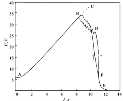
The typical dependence of voltage changes of de- formed tungsten wire conductor from current in mode of stabilization on Figure 3 is shown.
[image:3.595.331.511.155.480.2]The plastic deformation of tungsten wire was carried out at the room temperature. The curve ABCDEF (see
Figure 3) is composed from three parts with different
electrical resistivity. The deviation of U from its constant value on the segment AB is connected with the heating of wire and increasing its resistance. The dashed curve BC
corresponds to the dependence of electrical resistance from temperature for not deformed conductor or for an- nealed after its deformation at T > 0.5Tm within the time more than 103 s. Here Tm is melting temperature.
At the increasing of current density for deformed con- ductor on the segment AB at the average velocity greater than 2 × 10⁵ A·cm–2·s–1 the voltage U deviates from curve
AC in the point B. The characteristic value of the exter- nal electric field Ec is the magnitude about 102 V/m. On
the part of the curve BD on Figure 3 is shown that the voltage on the conductor decreases. The characteristic oscillations of dependence U (I) are observed also.
Length of the BD depends on the type of the metal and its degree of deformation. The curve BF is constructed for the velocity of current density growth equal to 5 × 10⁵ A·cm–2·s–1. On the segment DE the reduction of resis-
tance is even more pronounced than on the previous one. At the point F the resistivity ρ of deformed wire is ap-
proximately in 22 times less than at the point A. With further increase of current density, the resistivity ρ tends to zero. This corresponds to decrease of electrical resis- tance in 30 - 100 times. With increasing of current den-sity the good electrical hysteresis is manifested.
(a)
[image:3.595.322.520.530.693.2](b)
Figure 2. Characteristic dependences of current changes in time in pulse mode for: (a) Tungsten monospiral 0.05 mm; (b) Copper wire 4 mm.
The dislocation density in the cylindrical monospirals obtained by plastic deformation, calculated using the formula:
cosk n
b r h
(3)
where n: the dislocation density; b: Burger’s vector; r: mean radius of monospiral; h: the diameter of the con- ductor; β: angle between the line of the middle circle of monospiral and the plane slip of dislocation; k: the rela- tion of the conductor diameter to the inside diameter of monospiral.
Verification of the dislocation density was performed with an electron microscope, and then was determined the transition temperature of the conductor into super- conducting state. The critical transition temperature into SC state and the conditions for this transition was calcu- lated using the formula:
lg
m cr
c
cr cr
t t
j n
n j
(4)
where: tcr: critical transition temperature into SC; tm: melting temperature of the conductor; ncr: the critical density of dislocations for transition into SC; n: the dis- locations density in the conductor; jcr: the critical current density for transition into SC; jc: the velocity of current density growth in the conductor.
Formulas (3) and (4) allow to calculate all the pa- rameters necessary for the converting the metal wire into superconducting state. For example, we need a transition temperature into state of SC at the 1250˚C. According to formula (3) we calculate the necessary dislocation den- sity for the tungsten wire and define that it should be 5.7 × 1010 cm–2. Calculated diameters of cylindrical mono-
spirals for tungsten wires of two diameters 0.025 and 0.050 mm should be accordingly 0.081 and 0.130 mm.
Note, that by plastic deformation can be achieved the dislocation density not greater than 1 × 1014 cm–2. At this
density of dislocations the transition temperature for the conductor into superconducting state is quite high. The dependences of transition temperature into supercon- ducting state from the dislocation density and the veloc- ity of current density growth in three-dimensional space
on Figure 4 are shown.
When the dislocation density 1 × 108 cm–2 and the ve-
locity of current density growth 2 × 10⁵ A·cm–2·s–1 the
transition temperature into superconducting state for tungsten is 3410˚C. The magnitude of the dislocation density 5 × 1015 cm–2 is the experimental result achieved
by heat treatment of metallic conductors. With this dis- location density the transition of the conductor into super- conducting state occurs at the room temperature (20˚C).
The magnitude of the dislocation density 1 × 1015 cm–2
mechanically (by plastic deformation) can’t be reached because of saturation, however, thanks to the heat treat- ment in experiments at the velocity of current density growth 1 × 10⁴ A·cm–2·s–1 we are able to get repeatedly
the transition into superconducting state at 10˚C - 20˚C. Stable results correspond to the three-dimensional diagram
(Figure 4) and are the magnitudes specified on Table 1.
Thus, by means the heat treatment of conductor can be increased the dislocation density to values of about 1 × 10¹⁵ - 2 × 1015 cm–2, which reduces the temperature of
transition into superconducting state.
[image:4.595.312.538.313.495.2]Similar investigations were conducted with wires from other metals such as copper, nickel, aluminum, tantalum, molybdenum. They are showed that by heat treatment is possible to achieve such density of dislocations which decreases the threshold for the transition of metal into superconducting state (see Table 2).
Figure 4. Three-dimensional diagram of dependence of dis- locations density, velocity of current density growth and transition temperature of monospiral conductor into super- conducting state.
Table 1. Dependence of dislocations density, velocity of cur- rent density growth and transition temperature into super- conducting state for tungsten.
Dislocations density
cm–2
Velocity of current density growth
А·cm–2·s–1
Transition temperature into superconducting state
˚C
1 × 10¹⁴ 1 × 10⁴ 500
1 × 10¹⁴ 2 × 10⁵ 20
1 × 10¹⁵ 1 × 10⁴ 100
[image:4.595.308.539.597.724.2]Table 2. Dependence of dislocations density, velocity of cur- rent density growth and transition temperature into super- conducting state for some metals.
Materials Cu Ni Al Тa Mo
Dislocations
density, cm–2 1 × 10¹¹ 9 × 10¹⁰ 1 × 10¹³ 3 × 10¹¹ 9 × 10¹⁰
Velocity of current density growth,
А·cm–2·s–1 1 × 10
5 2 × 10⁵ 1 × 10⁵ 6 × 10⁴ 1 × 10⁵
Transition temperature
into SC state, ˚C 900 1300 600 2000 2000
5. Discussion
An explanation of described phenomenon in the frame- work of classical electronic theory, as well as within the well-known BCS-theory of superconductivity is not pos-sible, therefore we can suppose about some another type of superconductivity in metals. The authors propose that this phenomenon can be explained from the standpoint of dislocation theory.
Firstly about it says that the conductor prepared by this method has the form of infinite monospiral and it means that it has the form of infinite linear inductance in which at the certain parameters the own magnetic field is equal the zero, and, hence, absent of limit on infinite growth of current density in the conductor. It is known that both for usual low-temperature superconductors and for HTSC- superconductors the magnetic field is one of the impor- tant parameters limiting their applying by density of cur- rent. The second positive moment of such type of super- conductivity for the conductor having the form of mono- spiral is its high flexibility without destruction of super- conducting structure of metal, in difference from HTSC-2 cable having a heightened fragility of current-carrying ceramics. In this case are absent the limits practically for diameter of wire, let alone that is eliminated the neces- sity for cryogenic technology.
It was been established experimentally that at the ap- proach of dislocations density up to 1 × 1015 cm–2 and at
the maximum velocity of current density growth (2 × 10⁵
А/cm2·s) it is possible to provide the transition into su-
perconducting state at –50˚C (223 K). Increasing of dis- location density from 1 × 10⁸ to 1 × 1015 cm–2 was ob-
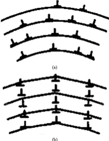
tained by heat treatment of wire, deformed preliminarily mechanically. The samples were specially deformed by their twisting into monospiral with an inner radius of curvature, tending up to zero. Thus, the geometrical re- distribution of atoms is occurred on the inner (small cur- vature) and outer (large curvature) surfaces, which form a kind of dislocations walls or so-called dislocations planes. These walls are formed by infinite parallel edge
dislocations with equal Burger’s vectors that are de- scribed, for example, by M. A. Shtremel [8] and Zh. Friedel [9].
Heat treatment (the polygonization) as a result of slip and climb of dislocations is the process of dividing the grains into fragments. Polygons and groups of dislocations of identical characters are grouped into the walls (Figure 5).
The formed planar dislocation walls are inactive and very stable. With further heating, they are retained al- most to the melting point of metals. After the formation of subgrain structure the recrystallization process is not occurred. At the passing an electric current through a metal conductor twisted into monospiral with a large radius of curvature and at the velocity of current density growth more than 100 A·cm–2·s–1, the passage of
elec-trons occurs between the formed walls of dislocations- waveguides.
When heated, the deformed twisting conductor over 3000˚C, in it formed the single-crystal blocks along the conductor length of 0.5 to 2 diameters of the wires with high dislocation density, which can be observed in the microscope. The wire thus becomes not round and repre- sents packing of blocks located along a wire. These blocks have the various forms depending on degree of curvature and owing to high density of dislocations. A lot of dislo- cation planes forming the waveguides for current flow are generated by twisting the wire in the form of cylin- drical monospiral with certain parameters.
(a)
(b)
[image:5.595.330.516.444.683.2]The principle of current flow in the channels formed with such dislocation planes in the metals deformed in this manner is similar to a passage of light in the fiber- optical cable used for transmission over long distances without loss of luminous flux.
The flow of current during the transition it from “su- perconductor” to the copper wire is accompanied by the melting area of the copper wire of length 10 - 30 cm. And this despite the fact that the density of transmitted current is in ten times lower than the current density, which can warm up this conductor to the temperature of 50˚C - 150˚C. Attention is drawn to the fact that itself this me- tallic superconductor has the ambient temperature, i.e.
about 25˚C - 30˚C. The facts of transition an electronic current from metallic monospiral superconductor to usual copper conductor having flexures are interesting also. The melting of copper wire is occurred on the larger radius of curvature, but the smaller radius remains un-changed, which also confirms the non-classical version of the electrons motion.
If for metallic superconductor is applied the direct current, it is heated the copper wire feeding with a posi- tive potential, while the lead wire with negative potential is not warmed up.
Note, that if the helix is heated by way of electric cur- rent in an inert atmosphere up to temperature 2500˚C, then the monospiral pass into the state of superconduc- tivity, and the temperature of the helix is reduced up to room temperature and it will be in the SC state so long as in it the current is flowing.
To reduce the time required to reach the transition of the conductor into SC state at the room temperature is necessary to use an external heat source up to 3000˚C. Several thousand samples was verified experimentally on the stability of conductors transition into SC state as a functions of heating temperature, velocity of current den- sity growth and dislocation density.
The measuring of transition temperature into super- conducting state on voltage-current characteristics was conducted for improvement of thermal tempering meth- ods with the purpose of magnification of dislocations density due to polygonization process and for control of dislocations density. Moreover, for each specific sample the transition temperature persists for the multiple (up to 10,000 cycles) transition of the conductor into the state of SC and back with an accuracy of 0.01%.
Methods of heat treatment may be different: the heat- ing by electric current, ion current, plasma discharges, laser, etc. It must ensure that the main objective is the achievement of the dislocation density required for the
transition of the conductor into superconducting state. In metallic superconductors of this type were obtained ex- perimentally the current densities up to 1 - 2 billion A·cm–2, which exceeds in 20,000 times the current
den-sity attainable for low-temperature metallic supercon-ductors.
6. Conclusions
The model for achieve the SC state in metals at positive temperatures considered in the paper based on the crea- tion in the metallic conductor channels for unobstructed passage of current, whose formation in the form of evenly spaced along the length of dislocation planes is provided by plastic deformation of the torsion and sub- sequent heat treatment.
The proposed method of converting the metallic con- ductor into superconducting state at the positive tem- peratures and particularly at temperatures close to the room temperature opens up principally new opportunities and perspectives of using these materials in various fields of industrial production and energy.
REFERENCES
[1] G. А. Markov, N. V. Melnikova and Y. A. Khon, “The Anomalously High Conductivity of Deformed Metals,” Letters to JTPh, Vol. 22, No. 16, 2002, 1996. pp. 65-72. [2] Y. A. Khon, G. A. Markov and N. V. Melnikova,
“Anomaly High Electrical Conductivity of Deformed Metals for High Electric Current Density,” Proceedings of International Conference of Role of Mechanics for Development of Science and Technology, Beijing, 13-16 June 2000, pp. 639-640.
[3] V. Buckel, “Superconductivity,” Mir, Moscow, 1975, p. 364.
[4] V. L. Ginzburg and D. A. Kirzhnic, “Problem of High- Temperature Superconductivity,” Nauka, Moscow, 1977, p. 400.
[5] G. A. Markov, “Method of Converting Metal Conductor into Superconducting State,” Patent No. 2233349 RU, 2002.
[6] G. А. Markov, “Method of Creation Abnormally Con- ductivity,” Patent No. 1826744 RU, 2009.
[7] G. А. Markov, “Method of Creation Abnormally Con- ductivity,” Patent No. 2061084 RU, 2010.
[8] М. А. Shtremel, “Toughness of Alloys. Part 1. Defects of the Grating. The Manual for High Schools,” Metallurgy, Moscow, 1982, p. 280.