A State Variable Method for the Realization of Universal
Current-Mode Biquads
Raj Senani1, Kasim Karam Abdalla2, Data Ram Bhaskar2
1Division of Electronics and Communication Engineering, Netaji Subhas Institute of Technology, Delhi, India 2Department of Electronics and Communication Engineering,
Faculty of Engineering and Technology, Jamia Millia Islamia, New Delhi, India E-mail: [email protected], [email protected], [email protected]
Received May 26, 2011; revised July 14, 2011; accepted July 21, 2011
Abstract
A state variable method of converting single-resistance-controlled-oscillators (SRCO), into universal cur-rent-mode biquad (offering realizations of all the five standard filter functions namely, low pass, band pass, high pass, notch and all pass) has been highlighted. The workability of the exemplary implementation of the derived current-mode universal biquad has been demonstrated by PSPICE simulation results based upon 0.35
μm technology. It is expected that the proposed method can be applied to other SRCOs to generate other
multifunction filter structures.
Keywords:Analog Electronics, Circuit Theory and Design, Current Mode Circuits, Universal Biquads, Current Conveyors
1. Introduction
Current-mode universal filters employing current con-veyors (CC) and their many variants have been exten-sively investigated during the past two decades for in-stance, see [1-19] and those cited therein. Current-mode universal filters can be broadly classified in two catego-ries namely the single input multi-output (SIMO)-type ([11-18]) and the multiple-input-single-output (MISO)- type ([5,10,14,19]). It may be mentioned that while most of the proposers of current-mode (CM) universal filters have come up with a specific topology rather than dis-closing any general method of systematic derivation of such filters. It may also be noted that while a general method for realizing SIMO-type CM universal filters has been known earlier [20], to the best knowledge of the authors, any systematic method of synthesizing MISO- type CM universal biquads has not been reported explic-itly in the open literature yet. The purpose of this paper is to fill this void.
The main object of this paper is to present a state vari-able method by which a given single resistance con-trolled oscillator (SRCO) can be re-configured as a mul-tiple-input-single-output (MISO)-type current-mode (CM) universal biquad. Although the method to convert a SRCO into universal current-mode biquad proposed here
might appear simple but it has not been explicitly pub-lished in the open literature earlier.
2. The Proposed Method
Although the proposed method is quite general and can be applied to any given SRCO using any kind of active element, we illustrate the method by choosing an earlier proposed SRCO as an example using fully differential second generation current conveyor (FDCCII) as an ac-tive element.
It may be recalled that a FDCCII and its applications for analog VLSI were introduced by El-Adawy, Soliman and Elwan in [1]. FDCCII has since then been used in realizing various signal processing and signal generation circuits for instance, see [1-6]. Simultaneously, improved implementations of FDCCII have also been advanced; see [7] and [8].
Some time back, Chang, Al-Hashimi, Chen, Tu and Wan [2] presented two novel single-resistance-controlled- oscillators (SRCO) using a single FDCCII and all ground- ed passive elements, which is advantageous for inte-grated circuit implementation.
R. SENANI ET AL. 287
(FO) is given by 0 2 3 1 2
With all its y-input terminals unconnected, the circuit can be redrawn as shown in Figure 1(a).
1
R R C C .
Note that with Y1 connected to Z and 3
con-nected to
Y Z with Y2 and Y4 connected to ground,
one obtains the SRCO of Figure 1 of [2].
To synthesize a filter providing independent control of
0
(say, by the resistor 2) and independent control of
bandwidth (
R 0/Q0
) (say, by the resistor R1), one must have a transfer function ( )
( )
out in
I N s
I D s with its
character-istic polynomial D s( ) given by
2 0 2 2
0
0 1 2 1
1
( ) s
D s s s s
Q R C C
C R R2 2 3
(1)
From the above, the characteristic equation of the circuit (assuming zero input) is given by
2
1 2 1 2 2 3
1 0
s s
R C C C R R
(2)
It can be easily worked out that assuming that the cir-cuit to be synthesized has to have two capacitors and three resistors only, if the voltages across the assumed capacitors C1 and C2 are taken as x1 and x2 respectively
FDCCII C1
1
R3
2
R C2
Y1 X+ 3 Z+ Z-4 2 Y Y Y
X-R Y
V1VY2VY3 YV4
x-i
x+
i i
z-z+ i x1 x2 + -+ -x+ V x-V (a)
FDCCII C1
1 R3
2
R C2
Y1
X+ 3
-Z+
Z- i1
i3
4 2
Y Y Y
X-R
i i2
4 -Z- io
(b)
Figure 1. (a) Circuit arrangement with un-committed
y-inputs of FDCCII, derived from SRCO of [2]; (b) An
ex-emplary MISO-type universal CM biquad.
such a circuit should be characterized by the following matrix state equation
1
1 2 1
2 2
2
2 3 2 1
1
d 0
d [ ]
1 1 d d x
C R x x1
t A
x x
x
C R C R
t
(3)
so that the consequent characteristic equation
0det s I A (4) would, indeed, result in the characteristic Equation (2).
Equation (3) can now be re-arranged as follows:
1 2 1 2 d d x x C
t R (5)
2 1 2 3 1 d d 2
x x x
C
t R R (6) The above equations can be considered to be the node equations (NE) of the circuit to be synthesized. In view of the FDCCII characterization, which is given by the equations: iYk 0,k = 1 - 4; ,
1 2 4
X Y Y Y
1 2 3
( )
X Y Y Y
v v v v
( )
v v v v , i Z iX, Z X , the cir-
cuit shown in Figure 1(a) ( where terminal Z+ is re-placed by –Z+) is characterized by the following equa-tion
i i
1 1 2 2 2 1 1
1 2 1 2 1 2 2
3
2 3 2 3 2 3 4
d 0 0
d 1
0 d
d
1 1 0 1
1 1 1
0 Y Y Y Y x x t x x C R t v
C R C R C R v
v
C R C R C R v
(7)
where voltages across capacitors 1 and C2 are cho-sen as state variables 1
C
x and x2 respectively. If the various Y-terminal voltages of FDCCII are chosen as:
1 0
Y
v , vY20, vY3x1, vY4x2 (8)
then it can be verified that resulting state equations will be same as in Equations (5) and (6).
After having made the above state variable assign-ment and by appropriately connecting the required ex-ternal terminals of the FDCCII in accordance with the requirements in Equation (8), a non-autonomous circuit with multiple-inputs and single-output (MISO) is subse-quently created by augmenting the circuit with four ex-ternal current input signals 1 2 3 and 4 and
extend-ing the FDCCII to have one additional Z+ output termi-nal (henceforth to be referred as multiple output FDCCII (MO-FDCCII)). The output current of the resulting
cir-, cir-,
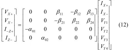
[image:2.595.80.265.398.681.2]cuit (shown in Figure 1(b)) is found to be:
11 12 13
21 22 24 1
01 2
02 3
4
0 0
0 0
0 0 0 0
0 0 0 0
X X X X Y Z Y Z Y Y I V I V V I V I V V
23 2 4 1
2 1 2 2 1 2 2 3
0
2
2 1 1 2 2 3
1
1
s s
i s i i i
C R C R C C R R
i
s s
C R C C R R
(9)
(12)
Note that the D(s) of (9) is exactly same as (1). The five filter responses can be realized from the cir-cuit of Figure 1(b) as follows: Low pass (LP): making
2 3 4 and taking i1 in. Band pass (BP):
making 1 3 and taking one of 2 or 4as in.
High pass (HP): making and taking or
1 along with
2 . Notch: making 2 or 4 1 along with 2 1. All pass (AP):
making along with .
0 i i i
i i
4 3 in
i i i
3 in
i i i i i i
i 1 0 i 1 R R 0 i
i i i
2 i i R i R
Taking Equation (12) into consideration, the non-ideal expression for the output current is given by (13)
Considering above, the non-ideal expressions for o,
and
o
Q H0 are found to be:
01 02 13 24 1 2 2 3
o C C R R
; 2 01 02 13 24
1
1 2 3
o
C
Q R
C R R
(14)
1 2 3 4 in 2 1
The various parameters of the realized filters are given by
i
R R
The non-ideal gains and realization conditions (wher-ever applicable) are modified as follows:
0LP
H = –1 (remains unaffected by non-ideal volt-age/current gains)
0
1 2 2 3
1 C C R R
;
2 1
1 BW
C R ;
2 1
1 2 3
o
C
Q R
C R R
0BP
H = 1
01 02 24 2 R R . (10) 1 2 0 for BP
1, for LP / HP / AP / Notch
R R
H (11) modifies to H0HP = 01 24 102 ; where the condition of realization R R2.
H0Notch= –1, if 02 = 1; realization condition being
same as in HP. where ω0 = cut-off frequency in radian/sec, BW =
band-width, Qo= quality factor and H0= gain. In the last
three cases, having fixed the bandwidth (BW) by 1, 0
R
can be independently controlled by 3 while in the
first two cases 0
R
(with 2 and/or ) and BW (by
) are independently adjustable.
R R3
1 R
0AP
H = –1, if 0102 24 1 and R2R1. From the above, the active and passive sensitivities of the non-ideal 0 and Qoare given by
1 2 2 3
1 2
o o o o
C C R R
S S S S ,
01 02 13 24
1 2
o o o o
S S S S , 1o 0,
R
S
3. Analysis Incorporating Nonideal
Parameters
2 01 02 13 24
1 2
o o o o o
Q Q Q Q Q C
S S S S S , Considering the non-ideal MO-FDCCIIs sources, two
parameters, and (where (1 i)and (1 v)
, with i( i 1
1 2 3
1 2
o o o
Q Q Q C R R
S S S , Q1o 1 (15)
R
S
)
and v( v1) denote the
current and voltage tracking errors respectively) need to From Equation (15) the active and passive sensitivities of oandQo are found to be in the range
1 1 2 F x S ,
and the circuit, thus, enjoys low sensitivities. be considered. Incorporating these sources of error, we
have the following non-ideal characterization of the MO-FDCCII:
2 01 02 13 24
02 3 02 24 01 2 4 1
2 1 2 2 1 2 2 3
0
2 01 02 13 24
2 1 1 2 2 3
s s
i s i i i
C R C R C C R R
i
s s
C R C C R R
(13)
1Although additional circuitry e.g. a multiple-output current follower will be needed at the front end of the proposed universal CM filter circuits to
[image:3.595.316.540.87.174.2] [image:3.595.61.286.91.160.2]R. SENANI ET AL. 289
4. Simulation Results
To verify the validity of the proposed configuration, cur-rent mode filters have been simulated in SPICE by mak- ing a CMOS MO-FDCCII based upon the FDCCII from [3] (Figure 3 therein) which is shown here in Figure 2.
PSPICE simulation implementation was based upon a CMOS MO-FDCCII in 0.35 μm technology where the aspect ratios of the MOSFETs are shown in Table 1.
The CMOS MO-FDCCII was biased with DC power supply voltages VDD = +1.5 V, VSS = −1.5V, IB =
35 μA, ISB = 100 μA, bp = 0.2 V, and bn = −0.66
V. To achieve the filters with o
V V
f = 1 MHz, the compo-nent values chosen were = = 0.71 k, 3 =
1.39 k , and C1 C2 . The frequency
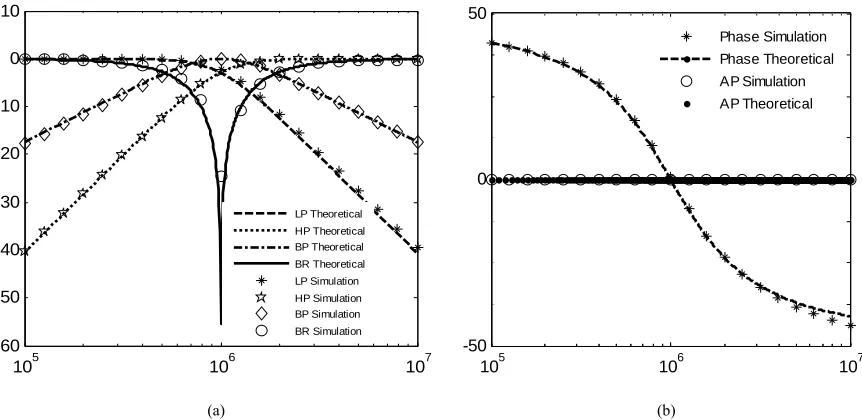
re-sponses of LPF, BPF, HPF, Notch and APF are shown in Figure 3. Thus, a very good correspondence between
1
R 0.
F2
R 16
R
n
theoretical values and PSPICE simulations is observed. To test the input dynamic range of the proposed filters, the simulation of the band-pass filter as an example has
been done for a sinusoidal input signal of fo = 1 MHz.
Figure 4 shows that the input dynamic range of the filter extends up to amplitude of 300 μA without significant distortion. The dependence of the output harmonic dis-tortion on the input signal amplitude is illustrated in Figure 5.
Although FDCCII-based filters have been proposed by many authors as [1,3-6], with the exception of [1] (Fig-ure 11therein), [6] (Figure 2 therein), all others deal with voltage-mode filters.
In view of this, a comparison with MISO-type CM universal biquads using FDCCIIs presented recently in [1] (Figure 11 there in) and [6] (Figure 2 therein) is now in order. When compared with the circuit of [1], the circuit of Figure 2 has the advantage of using only one active building block (one FDCCII) as against three FDCCII’s in biquads proposed in [1] and use of all grounded pas-sive elements (AGPE) which is an attractive feature for IC implementation. On the other hand, when compared with the circuit of [6] (Figure 2 there in) our circuit has
1
2
4
3
M
M M M M
M M
M
M M
M
M M
M
M M
M
M M
M M
M M
M
M
1 2
3 4 5 6
8 9
10 1
1
1 1
1
1 1 1
1
2
2 2
2
2
2 3
4
5
6
7 8
9
1
7
8 7
Z-4
0
M
M
M2 2
2
2
5
M2
4
M2 M4
4
M
4
M
4
M
1
3
3
1 0
M3 M 3
M3
M3
M3
M3
M3
M3
M3
4 3 7
6 9
5 8
4
M0
2 9
-Z+ X+ Y3Y1 Y2 Y4
X-Vbp
Vbp
Vbn Vbn
V
DD
V
SS SB
[image:4.595.66.535.341.560.2]I B I
[image:4.595.126.471.610.723.2]Figure 2. CMOS realization of the FDCCII.
Table 1. Aspect ratios of MOSFETs.
MOS transistors W/L
M1 - M6 0.7/0.35
M7, M8, M9, M13 15/1.2
M10, M11, M12, M24 0.7/0.35
M14, M15, M18, M19, M25, M29, M30, M33, M34, M37, M38, M39, M40 20/0.35
M16, M17, M20, M21, M26, M31, M32, M35, M36, M41, M42, M43, M44 25/0.35
105 106 107 -60
-50 -40 -30 -20 -10 0 10
LP Theoretical HP Theoretical BP Theoretical BR Theoretical LP Simulation HP Simulation BP Simulation BR Simulation
105 106 107
-50 0 50
Phase Simulation
Phase Theoretical AP Simulation
AP Theoretical
[image:5.595.81.512.85.295.2](a) (b)
Figure 3. PSPICE simulation results. (a) Gain response of LPF, BPF, HPF and Notch. (b) Gain and phase response of APF.
3.7 3.75 3.8 3.85 3.9 3.95 4
x 10-5 -4
-2 0 2 4x 10
-4
Time (s)
Am
pi
tu
de
(
A
)
[image:5.595.123.475.329.486.2]Iin Iout
Figure 4.Input and output waveforms of the band-pass filter of the proposed circuit for 1 MHz sinusoidal input current of 300 μA.
0 1 2 3 4 5 6 7 8 9 10
10 30 50 70 90 110 130 150170 190210 230250 270 290 310 330350 370 390
Iout (uA)
T
HD %
[image:5.595.148.449.525.692.2]R. SENANI ET AL. 291
the advantages of independent tunability of BW or Qo
which is not feasible in the quoted circuit of [6] which also needs two outputs to implement APF. Our FDCCII has nine terminals in contrast to the FDCCII in [6] which has eleven terminals to implement the biquad filter.
The comparison with [9] and [10] is now in order, The circuit of [9] (Figure 8 there in) is also current-mode MISO type and uses five grounded passive elements but used two FDCCIIs (the first has ten terminals and the other has nine terminals to implement the biquad filter) and not independent tunability of BW or Qo.
The circuit of [10] although uses one FDCCII (eleven terminals to implement the biquad filter in current –mode and voltage mode) but has one floating resistance and needs two outputs to implement LPF and APF.
5. Concluding Remarks
A method has been presented by which the FDCCII- based CM SRCOs of [2] can be reconfigured as MISO-type universal biquads offering realizations of all the five standard filter functions also, thereby enhancing their capabilities. One exemplary biquad resultingfrom the application of the proposed method was presented and its workability was demonstrated by SPICE simula-tion using an FDCCII implementasimula-tion in 0.35 μm CMOS technology.
The methodology presented here could also be applied to all other SRCOs published earlier using other kinds of active building blocks thereby giving rise to a large number of new MISO-type CM universal biquads, some of which may possess some interesting features. This, however, is left for further investigations.
6. Acknowledgements
The authors wish to thank an anonymous reviewer for his constructive feedback, which has been helpful in im-proving the presentation. The material presented here has its origin in an earlier unpublished report2 of Analog Sig-
nal Processing Research Lab of NSIT, where part of this work was performed.
7. References
[1] A. A. El-Adawy, A. M. Soliman and H. O. Elwan, “A Novel Fully Differential Current Conveyor and Its Ap-plications for Analog VLSI,” IEEE Transactions on Cir-cuits and Systems II: Analog and Digital Signal Process-ing, Vol. 47, No. 4, April 2000, pp. 306-313.
doi:10.1109/82.839666
[2] C. M. Chang, B. M. Al-Hashimi, H. P. Chen, S. H. Tu and J. A. Wan, “Current Mode Single Resistance Con-trolled Oscillators Using Only Grounded Passive Ele-ments,” Electronics Letters, Vol. 38, No. 39, 2002, pp. 1071-1072. doi:10.1049/el:20020714
[3] H. P. Chen, “Single FDCCII-Based Universal Voltage- Mode Filter,” International Journal of Electronics and Commun (AEU), Vol. 63, No. 9, 2009, pp. 713-719. doi:10.1016/j.aeue.2008.05.012
[4] F. Gür and F. Anday, “First-Order Allpass Sections- Based High-Input Low-Output Impedance Voltage-Mode Universal Filter Using FDCCIIs,” Proceeding of 18th European Conference on Circuit Theory and Design, Seville, 27-30 August 2007, pp. 428-431.
[5] C. M. Chang and H. P. Chen, “Single FDCCII-Based Tunable Universal Voltage-Mode Filter,” Circuits Sys-tems Signal Processing, Vol. 24, No. 2, 2005, pp. 221- 227. doi:10.1007/s00034-004-0422-7
[6] C. M. Chang, B. M. Al-Hashimi, C. L. Wang and C. W. Hung, “Single Fully Differential Current Conveyor Bi-quad Filters,” IEE Proceeding of Circuits Devices System, Vol. 150, No. 5, 2003, pp. 394-398.
doi:10.1049/ip-cds:20030468
[7] S. A. Mahmoud, M. A. Hashiesh and A. M. Soliman, “Low-Voltage Digitally Controlled Fully Differential Current Conveyor,” IEEE Transactions on Circuits and Systems I, Vol. 52, No. 10, 2005, pp. 2055-2064. doi:10.1109/TCSI.2005.852922
[8] H. A. Alzaher, “CMOS Highly Linear Fully Differential Current Conveyor,” Electronics Letters, Vol. 40, No. 4, 2004, pp. 214-216. doi:10.1049/el:20040183
[9] F. Gür and F. Anday, “Simulation a Novel Current-Mode Universal Filter Using FDCCIIs,” Analog Integrated Circuits and Signal Processing, Vol. 60, 2009, pp. 231- 236. doi:10.1007/s10470-009-9293-y
[10] C. N. Lee and C. M. Chang, “Single FDCCII-Based Mixed-Mode Biquad Filter with Eight Outputs,” Interna- tional Journal of Electronics and Communication (AEU), Vol. 63, No. 9, 2009, pp. 736-742.
doi:10.1016/j.aeue.2008.06.015
[11] R. Senani and A. K. Singh, “A New Universal Current- Mode Biquad Filter,” Frequenz, Vol. 56, 2002, pp. 55-59. [12] R. Senani, A. K. Singh and V. K. Singh, “New Tunable
SIMO-Type Current-Mode Universal Biquad Using Only Three MOCCs and All Grounded Passive Elements,” Frequenz, Vol. 57, 2003, pp. 160-161.
[13] J. W. Horng, “Current Conveyor Based Current-Mode Universal Biquadratic Filter,” Journal of the Chinese In-stitute of Electrical Engineering, Vol. 9, 2002, pp. 147- 150.
[14] H. Y. Wang and C. T. Lee, “Versatile Insensitive Current Mode Universal Biquad Implementation Using Current Conveyors,” IEEE Transactions CAS-II. Analog and Digital Signal Processing, Vol. 48, 2001, pp. 409-413.
2R. Senani, “Re-Configuring FDCCII-Based SRCOs into Universal
Current mode Biquads”, TCASII ID-2267, November 14, 2003 (Unpub-lished).
DO-CCCIIs and OTA,” Circuits Systems and Signal Pro- cessing, Vol. 28, No. 1, 2009, pp. 99-110.
doi:10.1007/s00034-008-9072-5
[16] E. Yuce and S. Minaei, “Universal Current-Mode Filters and Parasitic Impedance Effects on the Filter Perform-ances,” International Journal of Circuit Theory and Ap-plications, Vol. 36, No. 2, 2008, pp. 161-171.
doi:10.1002/cta.418
[17] S. Minaei, “Electronically Tunable Current-Mode Uni-versal Biquad Filter Using Dual-X Current Conveyors,” Journal of Circuits, Systems, and Computers, Vol. 18, No. 4, 2009, pp. 665-680. doi:10.1142/S0218126609005186
[18] C.-M. Chang, B. M. Al-Hashimi and J. N. Ross, “Unified Active Filter. Biquad Structures,” IEE Proceeding of Circuits Devices System, Vol. 151, No. 4, 2004, pp. 273- 277. doi:10.1049/ip-cds:20040132
[19] R. Senani, “New Universal Current Mode Biquad Em-ploying All Grounded Passive Components But Only Two DOCCs,” Journal of Active and Passive Electronic Devices, Vol. 1, 2006, pp. 281-288.
![Figure 1. (a) Circuit arrangement with un-committed y-inputs of FDCCII, derived from SRCO of [2]; (b) An ex-emplary MISO-type universal CM biquad](https://thumb-us.123doks.com/thumbv2/123dok_us/9219350.409007/2.595.80.265.398.681/figure-circuit-arrangement-committed-fdccii-derived-emplary-universal.webp)