Scattered surface charge density: A tool for surface characterization
Borislav Naydenov,1,3Mauro Mantega,2,3Ivan Rungger,2,3Stefano Sanvito,2,3and John J. Boland1,3,*
1School of Chemistry, Trinity College, Dublin 2, Ireland 2School of Physics, Trinity College, Dublin 2, Ireland
3Center for Research on Adaptive Nanostructures and Nanodevices (CRANN), Trinity College, Dublin 2, Ireland
(Received 27 April 2011; revised manuscript received 1 September 2011; published 28 November 2011) We demonstrate the use of nonlocal scanning tunneling spectroscopic measurements to characterize the local structure of adspecies in their states where they are significantly less perturbed by the probe, which is accomplished by mapping the amplitude and phase of the scattered surface charge density. As an example, we study single-H-atom adsorption on then-type Si(100)-(4×2) surface, and demonstrate the existence of two different configurations that are distinguishable using the nonlocal approach and successfully corroborated by density functional theory.
DOI:10.1103/PhysRevB.84.195321 PACS number(s): 68.37.Ef, 73.20.At
I. INTRODUCTION
Many materials exhibit surface states that are effectively electronically decoupled from the bulk, and the presence of surface adspecies induces scattering and the formation of standing-wave patterns in the local density of states (LDOS). This phenomenon was first demonstrated on the Cu(111) surface through the pioneering work of Eigler et al.1 and Avouriset al.2 Here, we show that a spatial mapping of the amplitude and phase of these standing waves is extremely sensitive to the precise nature of the adsorption configuration. We demonstrate this sensitivity for the case of a single H atom on the Si(100) surface, for which in principle there exist two different adsorption configurations [see Fig1(a)]. It was previously reported that on a low-dopedn-type Si(001) at room temperature (RT), only a single metastable H-atom species is observed, which switches between the two configurations under the influence of the scanning tunneling microscopy (STM) bias polarity.3,4 Here we report on the case of heavily doped n-type Si(100) and demonstrate the presence of two distinguishable H-atom species, one of which is metastable and identical to that reported earlier,3,4 and the other being stable and unperturbed by the STM probe. Moreover, we demonstrate that both species are also distinguishable us-ing a combination of nonlocal, spatially resolved, scannus-ing tunneling spectroscopy (STS) and density functional theory (DFT) simulations, thus providing a new nonlocal approach for investigating surface structure and reactivity. Notably, a nonlocal measurement is less intrusive than a local one as the interaction between the scattering center and the STM tip is significantly reduced. As such, scattering centers, which switch at high frequency between different geometries under the influence of the STM tip, can be observed as stable in a nonlocal measurement.
The Si(100) surface is comprised of Si-Si dimers that are arranged in rows extending along the [110] directions, as shown in Fig1(a). The dimers tilt such that the charge density of the singly occupied dangling bond (DB) is transferred from the lower to the upper dimer atom. The pattern of dimer tilting is anticorrelated both along and across rows, yielding ac(4×2) reconstruction. A single hydrogen atom reacts predominantly with the Si dimer atoms leading to the final products HB or HT in which it is bonded to the lower or upper dimer atom
of the initially bare surface, respectively [see Fig.1(a)]. The subtle difference between these configurations thus provides an excellent test case for our strategy, which is summarized in Figs.1(b)and1(c), where we plot the simultaneously acquired traces of the topography (z) and differential conductance (dI /dV) along rows containing reacted dimers [dotted lines in Fig.1(a)]. While the topography traces are similar outside the reacted dimers, thedI /dV scans show the presence of standing waves5 with a significant phase difference for the two adsorbate configurations [compare the blue and red lines in Fig.1(c)]. As such, thedI /dV curve suggests that nonlocal spectroscopic data contain information about the adsorbate configuration. We demonstrate below that this information is sufficient to distinguish between different adsorption sites.
II. EXPERIMENTAL LAYOUT
All experiments were performed at 77 K using a Createc cryogenic STM system described elsewhere.6Semiconductor [Si(100),n-type:As, 0.001−0.005cm] samples were used.7 The atomic hydrogen source was a heated tungsten capillary. Electrochemically etched tungsten probes were annealed
in situand subsequently inked8using Pt or Al metal samples7 in the microscope. Variable-height scanning tunneling spec-troscopy (VH-STS)6was used for all STS measurements.
III. COMPUTATIONAL LAYOUT
(a)
Topography (
Å
)
dI/d (a.u.)
Majority Adspecies
Minority Adspecies
X Y
Z
(b)
(c)
FIG. 1. (Color) Schematics of the Si(100)-(4×2) surface with adsorbed single-hydrogen atoms are presented in (a) where the majority (HB) and minority (HT) configurations found in the experiment are marked. The minority adspecies concentration, when present (see Sec.II),
was always more than an order of magnitude smaller than the majority hemihydride concentration. STM topographic lines [dotted lines in (a)] taken along the middle of the reacted dimer rows with 20 pA and+0.5 V are plotted in (b), with blue for the majority and with red for the minority configuration and are also marked with dotted lines in (a). The differential conductance recorded simultaneously with the topographic lines in (b) are presented in (c) with corresponding colors.
of the c(4 × 2) reconstructed surface (each of which have a length of 7.566 ˚A and contain 88 atoms) along the dimer rows. In total, in the VASP simulation cell, we have 440 atoms for the clean surface, plus the one adsorbed hydrogen atom. A 12- ˚A-long vacuum region that is used to avoid interaction between periodic images and n-type doping is simulated by adding one extra charge to the supercell plus a uniform neutralizing background. Open-boundary-conditions calculations were performed with a newly implemented order-N version of SMEAGOL,10,13 which combines DFT with a recursive nonequilibrium Green’s function scheme built in the spirit of the embedding-potential method.14 We note that in this work, we use the code only at equilibrium, with the aim to avoid periodic boundary conditions along the dimer row, and therefore to simulate single impurities. The unit cell is constructed from the VASP-relaxed coordinates and it is 204.28 ˚A long along the dimer direction (2377 atoms). STM LDOS simulations are performed with the Tersoff-Hamann approach15 from the SMEAGOL electronic structure. The basis set used is doubleζ for the Si-s, Si-p, and H-sorbitals, and singleζ for the Si-dand H-porbitals.
IV. RESULTS AND DISCUSSION
During atomic hydrogen deposition, only HB adspecies were formed above 400 K surface temperature, whereas traces of the HT configuration appeared after RT deposition, with the population significantly increased below 250 K surface temperature. At low-hydrogen coverage, the HTconcentration was correlated to the presence of defects (concentration
1%) on the surface and was always more than an order of magnitude smaller than the HB concentration. Based on the above observations, we denoted the HB and HT as the majority and minority adspecies on then-type Si(100) surface,
respectively. This assignment was additionally supported by the computational result (see Sec. IVA below).
A. Local approach
[image:2.608.117.493.77.278.2](a) (b) (c) (d)
FIG. 2. (Color) Topographic images of a single-hydrogen atom chemisorbed on then-type Si(100)-c(4×2) surface. Filled-state (bottom) and empty-state (top) images are presented in (a) and (d), simulated with sample biases of−0.5 and+0.5 V, respectively. The corresponding experimental constant current (20 pA) images are shown in (b) and (c), recorded with sample biases of+0.5 V (top) and−1.0 V (bottom). Sketches of the Si dimer atoms are shown in parallel with the topographs, where big and small circles correspond to upper and lower Si dimer atoms, respectively. Bright symbols are used for the atoms dominating the images. Arrows indicate the dimer buckling adjacent to the reacted dimers. The hydrogen atom (green circles) and the dangling bond (red ellipses) are kept with the same orientation in all panels. On the bottom of the figure, large-area topographic images (20 pA) including the (c) majority and (b) minority (vertically flipped) adspecies are presented.
reported in the works of Reusch et al.3 and Radny et al.4 in the case of the single-H-atom species they observed on a low-doped Si(001) sample under RT STM imaging conditions.
In the case of the majority adspecies, good agreement between STM data and simulated images is obtained only for the case in which the H atom is placed in the HBposition [compare Figs.2(c)and2(d)]. In contrast, simulations for HT [Fig. 2(a)] predict a tilting pattern for the adjacent dimers, which is inconsistent with the experiments in Fig. 2(c) but consistent with those in Fig.2(b), i.e., with the minority sites. A careful comparison of the minority-site topographic data with the simulations for HBand HTreveals that the topography of the empty states behaves as though the H is located at the HTsite, whereas for the filled states, it is fully consistent with the HBsite. This confirms the fact that the entire dimer row is flipping. Our DFT calculations forn-doping conditions reveal that the HBconfiguration is lower in energy by 136 meV with respect to the HT one. This demonstrates that the majority configuration is indeed the lower-energy state, and that the minority one is metastable and stabilized by the pinning effect of neighboring defects. The stability of the majority species is not expected to vary for lower dopant concentrations, since calculations on the intrinsic neutral systems still show the HB lower in energy by 26 meV. These results are consistent
with the results obtained in the work of Reuschet al.3where, based on cluster calculations, the HBconfiguration was found lower in energy by 260 and 30 meV forn-type and intrinsic systems, respectively. Thus, while DFT topography and total-energy simulations provide unique interpretations of the STM data for the H/Si(100) system, in the more general case, different adsorbate configurations may not show significantly different STM topographic signatures, thus necessitating a more detailed investigation of the electronic structure.
B. Nonlocal approach
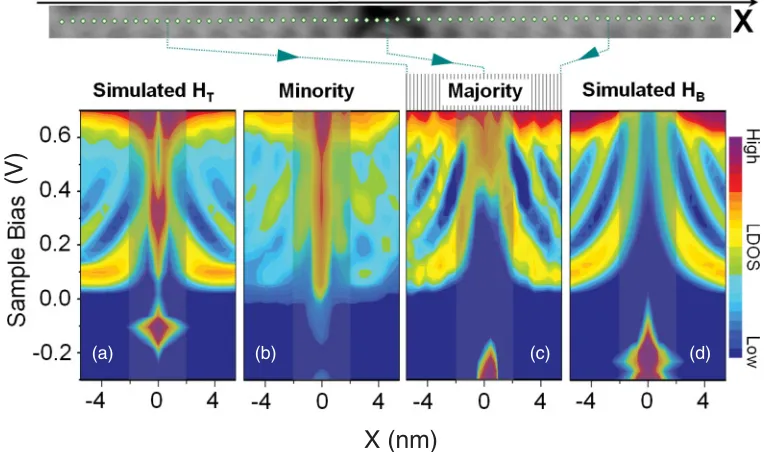
[image:3.608.116.495.69.355.2]X (nm)
(V)
(a) (b) (c) (d)
FIG. 3. (Color) Spatial LDOS maps of theπ∗standing waves along the Si dimer row with single-hydrogen occupied dimer atx=0. Shaded and nonshaded areas highlight the local and nonlocal approach discussed in the text. The map in (c) was constructed from LDOS spectra recovered6from experimentaldI /dV measurements taken on each point of the topographic image (top of the figure) along the dimer row (xordinate). The map in (b) was constructed as in (c). The same intensity (color) scale as in (b) and (c) was applied for the corresponding simulated LDOS maps in (a) and (d). All panels correspond to the configurations in the respective panels in Fig.2.
presence of reacted scattering sites. The experimental LDOS maps in Fig. 3 show that the π∗ band is strongly scattered by both types of H-atom species. We simulate the LDOS of both by plotting the SMEAGOL density of states as a function of the atomic position, and present them in Figs. 3(a) and 3(d) for the HT and HB configurations, respectively. In the calculations, the DOS of the top and bottom Si dimer atoms are combined to reflect the experimental conditions, where the measurements are made along the middle of the dimer row (top of Fig.3). Additionally, the theoretical bands in Figs.3 and4have been shifted by 0.125 meV in order to align the bottom of the conduction bands.
For the HB site, both the experiment and simulations [Figs. 3(c)and3(d)] reveal identical standing-wave patterns produced by a potential barrier and the presence of an intense doubly occupied DB signature, consistent with then+doping of the Si substrate.17In the case of the H
Tsite, however, the DB is singly occupied, as evidenced by the filled and empty DB features in Figs.3(a)and3(b). The associated standing-wave pattern is significantly altered, revealing a nonmonotonic phase variation of the scattered waves that suggests the presence of a resonance in the potential barrier at the energy close to the half-empty DB state. Again, the shape and position of the experimental HT pattern in Fig. 3(b) matches the simulated one in Fig.3(a). The excellent agreement between theory and experiments for the nonlocal (nonshaded areas in Fig.3) characteristics of the surface further strongly supports the assignment of the majority sites to the HB configuration [compare Figs. 3(c) and3(d)] and the minority sites to the HTconfiguration [compare Figs.3(b)and3(a)]. The absence of detected structural changes (dimer flipping) in the negative bias region in the spectra of the HTconfiguration [see Fig.3(b)]
is due to the fact that the threshold for dimer flipping observed in the topographs [Fig.2(b)] occurs at negative biases greater than−0.3 V sample bias.7
0 1 2 3 4
0.00 3.14 0.0 0.2 0.4 0.6 0.8 1.0
H
B
H
T
HB HT
Γ
J'
Θ
(rad)
k (nm-1)
Experiment
Theory
}
}
E (eV)
(b) (a)
[image:4.608.114.496.73.299.2] [image:4.608.353.519.421.660.2]It is possible to extract quantitative information from the LDOS scattering maps in order to definitively establish the identity of the majority and minority species. By measuring the wavelength of the oscillations in the LDOS for different energiesE,in Fig.3, we can obtain the band dispersionE(k) and phase shift(k) by fitting the LDOS as follows:
LDOS∝ |ψ(x)|2∝1+2 cos(2kx+), (1)
whereψis the surface-state wave function, andx=0 is set at the position of the H atom.E(k) is plotted in Fig.4(a)for data obtained from the maps of Figs.3(a)−3(d). The theoreticalπ∗ band dispersion along the dimer row for the bare surface is also plotted (dashed line) in Fig. 4(a). The dispersions obtained for the majority and minority sites agrees well with each other and the simulation for the HB and HT configurations, demonstrating that the scattering phenomena is an intrinsic property of theπ∗ band. However, the phase shifts(k) of the wave function scattered from the majority and minority sites are dramatically different and provide a unique signature, which is measured nonlocally and by which we can distinguish between the two H configurations. The majority-site phase shift [black spectrum in Fig.4(b)] decays monotonically with k, whereas the minority species [red curve in Fig.4(b)] show a different slope and a pronounced minimum associated with a resonance in the scattering barrier. A comparison with the simulated phase shifts associated with scattering from the HB (green) and HT (blue) sites establishes once again that these configurations can be assigned to the majority and minority species, respectively. The observed differences between the experiment and simulated phase shift for the minority site likely reflect the need for a stabilizing defect in the adjacent area, which was not accounted for in these simulations.
The experimental (black) and the simulated (green) results for the majority species show a(k) dependence that is ap-proximately linear with negative slope, suggesting a triangular-shaped barrier, in agreement with the displacement of the conduction-band edge around the scattering site [Figs. 3(c)
and3(d)]. For the minority configuration, the strong resonance in the barrier [shaded areas in Figs.3(a)and3(b)] is clearly detected in the phase-shift spectrum [red and blue curves in Fig.4(b)] and underlines the increased transmission coefficient at the resonance position, leading to significant reduction of the phase shift. Clearly, the latter reflects the fact that in the case of HT configuration, the dangling bond is half filled, causing it to interact with the scattered charge density.
V. SUMMARY
We have demonstrated the ability of the nonlocal spatial LDOS mapping to characterize surface adsorbate configu-rations. This nonlocal technique has been applied to study the majority and minority H-atom species adsorbed on the n-type Si(100)-(4×2) surface. The combined results obtained from experimental STS and DFT simulated data are supported by the local approach (adspecies electronic structure) and STM data. This nonlocal spatial LDOS mapping technique is a powerful addition to the standard STM tools, with the added advantage of being able to characterize systems in their nonperturbed states. As such, it is expected to be useful to investigate molecule and complex-surface configurations where topographic signatures of different configurations are indistinguishable or in instances where there are no STM-accessible states within the tunneling energy window. Further-more, as the nonlocal approach barely perturbs the scattering center, it can be used to characterize adsorbate geometries that are mechanically unstable under the STM tip.
ACKNOWLEDGMENTS
J.J.B. and S.S. acknowledge the Science Foundation Ireland funded Principal Investigator Awards (Grant No. 06/IN.1/I106, Grant No. 07/IN.1/I945) and CRANN. I.R. acknowledges funding from KAUST. Computational resources have been provided by the HEA IITAC project managed by the Trinity Center for High Performance Computing and by ICHEC.
1M. F. Crommie, C. P. Lutz, and D. M. Eigler,Science262, 218
(1993).
2P. Avouris,Solid State Commun.92, 11 (1994).
3T. C. G. Reusch, O. Warschkow, M. W. Radny, P. V. Smith, N. A.
Marks, N. J. Curson, D. R. McKenzie, and M. Y. Simmons,Surf. Sci.601, 4036 (2007).
4M. W. Radny, P. V. Smith, T. C. G. Reusch, O. Warschkow, N. A.
Marks, H. F. Wilson, S. R. Schofield, N. J. Curson, D. R. McKenzie, and M. Y. Simmons,Phys. Rev. B76, 155302 (2007).
5K. Sagisaka and D. Fujita,Phys. Rev. B72, 235327 (2005). 6B. Naydenov and John J. Boland,Phys. Rev. B82, 245411 (2010). 7See Supplemental Material at http://link.aps.org/supplemental/
10.1103/PhysRevB.84.195321 for extended experimental details together with photographs of the sample holders and large area images. Raw STS data are also presented and discussed in relation with the dimer flipping.
8B. Naydenov, P. Ryan, L. C. Teague, and John J. Boland,Phys. Rev.
Lett.97, 098304 (2006).
9G. Kresse and J. Hafner,Phys. Rev. B47, 558 (1993);49, 14251
(1994);G. Kresse and J. Furthmuller,Comput. Mater. Sci.6, 15 (1996); Phys. Rev. B54, 11169 (1996);G. Kresse and D. Joubert,
ibid.59, 1758 (1999).
10A. R. Rocha, V. M. Garcia Suarez, S. W. Bailey, C. J. Lambert,
J. Ferrer and S. Sanvito,Phys. Rev. B 73, 085414 (2006); Nat. Mater.4, 335 (2005);I. Rungger and S. Sanvito,Phys. Rev. B78, 035407 (2008).
11J. P. Perdew, K. Burke, and M. Ernzerhof,Phys. Rev. Lett.77, 3865
(1996);J. P. Perdew, J. A. Chevary, S. H. Vosko, K. A. Jackson, M. R. Pederson, D. J. Singh, and C. Fiolhais,Phys. Rev. B46, 6671 (1992);48, 4978 (1993).
12P. E. Bl¨ochl,Phys. Rev. B50, 17953 (1994).
13J. M. Soler, E. Artacho, J. D. Gale, A. Garcia, J. Junquera, P. Ordejon
14O. R. Davies and J. E. Inglesfield, Phys. Rev. B 69, 195110
(2004).
15J. Tersoff and D. R. Hamann, Phys. Rev. Lett. 50, 1998
(1983).
16M. Passoni, F. Donati, A. LiBassi, C. S. Casari, and C. E. Bottani,
Phys. Rev. B79, 045404 (2009).
17M. B. Haider, J. L. Pitters, G. A. DiLabio, L. Livadaru, J. Y. Mutus,