Abstract—In this paper an innovative design of an extremely low power and low current wireless communication system is proposed through hardware and software simulations. The system is operated at 200 KHz and the information is transmitted at extremely low rate of 40 KHz, its output is a 2.5 us pulse signal; it then uses this pulse signal as a carrier to transmit information. It uses this low frequency 40 KHz signal to save the power consumption. Finally it implements with Verilog hardware description language to design this low power wireless transmission system; it is then validated the design through ModelSim software simulation and finally the system is fabricated in the FPGA development platform.
Keywords—ModelSim, Verilog, Low Power Consumption, Wireless Transmission System.
I. INTRODUCTION
arious wireless transmission technologies and products have been developed and applied in our life and it is a trend of considering the design of low power wireless transmission systems in the future wireless communication system development. Wireless transmission products, especially the portable ones, have their advantages that their transmissions are not hindered by the communication environments. Meanwhile with the advancement of technologies the number of chips fabricated in the circuits is extremely large; consequently it becomes an important task in the future system development of how to design low power consumption products and to increase the usage length of products and the battery life.
II. SYSTEM ARCHITECTURE
As shown in Fig. 1 and Fig. 2 are the functional block diagrams of the transceiver, it has a LC oscillation circuit and
Hsien-Wei Tseng is with the Department of Computer and Communication Engineering, De Lin Institute of Technology, Tucheng City, Taipei County, Taiwan 23656, R.O.C. (e-mail: [email protected]).
Yang-Han Lee is with the Department of Electrical Engineering, Tamkang University, Tamsui, New Taipei City, Taiwan 25137, R. O. C. (e-mail: [email protected]).
Yih-Guang Jan is with the Department of Electrical Engineering, Tamkang University, Tamsui, New Taipei City, Taiwan 25137, R. O. C. (e-mail: [email protected])
Wei-Chien is with the Electronic Engineering Department, De Lin Institute of Technology, Tucheng City, Taipei County, Taiwan 23656, R.O.C. (e-mail: [email protected]).
Liang-Yu Yen is with the Department of Electrical Engineering, Tamkang University, Tamsui, New Taipei City, Taiwan 25137, R. O. C. (e-mail: [email protected]).
Wei-Chan Lee is with the Department of Electrical Engineering, Tamkang University, Tamsui, New Taipei City, Taiwan 25137, R. O. C. (e-mail: [email protected]).
this signal is passed through an amplifier; the 40 kHz carrier signal is continuously transmitted to save the system power consumption. The received signal after passing through an amplifier is sent to the digital circuit for further processing.
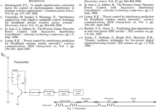
A. Transmitter
The transmitter, as shown in Fig. 1, consists of four parts and each part has its own function but they are all dependent on the front end, Session A, to generate various types of transmit signals [1].
The analog circuit of the transmitter is a LC oscillating circuit its inductance is 1.58 mH and its capacitance is 104pF and consequently its oscillating frequency is 40 kHz; the signal is radiated from the antenna after it passes through the oscillator.
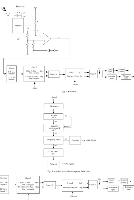
B. Receiver
As shown in Fig. 2, the received signal from the receiver antenna is passed through the front end analog LC oscillator circuit, its inductance is 4MH and the capacitance is 3.9 nF, with 40 kHz oscillating frequency. The other part is a self-generated 200 kHz clock; it is used as the network timing pulse and is transmitted together with the received signal to the later part of the digital circuit [2].
When the 40 kHz oscillating signal passes into the digital circuit it first enters into the debounce circuit to filter out the noise interference, when the high signal has duration than 7.5 us its output is high while when the low signal has duration longer than
7.5 us its output is low, in other words, the function of the debounce circuit is to delay the input signal by 7.5 us. The other part is the Check T, its main function is to detect the period length and to determine it is in the range of 20 ns and 30 ns and if it is it will output a 2.5us pulse. The third part is the counter to count how many 2.5 us pulses have been generated, it utilizes a counter and after counting 13 times to generate a 2.5 us pulse. The fourth part is to read twice of the 2.5 us pulses out the third part to generate a 2.5 us pulse and this is the output signal.
C. The Design of the Analog Circuit
The analog LC circuits in the transmitter and receiver have the oscillating frequency as calculated in Eq. (1).
Transmitter: L = 1.58mH C = 103 = 10*103PF ) ( 1 . 40 97 . 3 * 10 * 2 1 2 1 6 kHz LC
f
…….(1)
The oscillating frequency in the receiver terminal can be calculated from Eq. (2):
Receiver:L = 4mH C = 3.9nF
The Design of a Low Power Wireless
Transmission System
Hsien-Wei Tseng1, Yang-Han Lee2, Yih-Guang Jan3, Wei-Chien4, Liang-Yu Yen5and Wei-Chan Lee6
) ( 1 . 40 94 . 3 * 10 * 2 1 2 1 6 kHz LC
f
………. (2)
D. The Flow Chart of the System Operation
As shown in Fig. 3 is the wireless transmission system flow chart, it is used to demonstrate the operation of the receiver digital circuit. When the receiver receives the transmitted signal it is delayed by 7.5 us by the denounce circuit and is transmitted to the next stage circuit and it then uses the shift register to store the length of the period and to determine whether it needs to clear the shift register when the counter in the shift register is over 13. When the shift register has count of 13 it simultaneously triggers the F check to determine the length of the signal is between 265 us to 365 us when the counter has count 13. If the length is not in this range it outputs a wrong message. If it is then it next counts another 13 times signal to have a total of 26 times signal and it then generates a 2.5 us pulse signal.
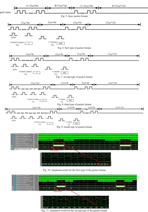
Fig. 4 is the resulting circuit after the above digital circuit has been modified to generate four different types of packet format signals as shown in Fig. 5-9. The four different types of packet format signals instead of only a fixed format signal can be generated in the original circuit but main function of the original circuit has been maintained. In Fig. 5 it depicts the first type of packet format, it is A session, B session, C session and D session respectively considered from the front end. The A session is 25 us *60 and is designed as a dynamic session that its length can be varied and is used as the control signal. Session B = 25 us * 40 and is used to carry the start the position of the information message, C session = 25 us *40 to carry the end location of the information message and D session = 25 us * 120 denotes the end location of the transmitted packet. The second format is A session = 25 us * 90, the third format is A session = 25 us * 120 and the fourth format is A session = 25 us * 140 [3]. As shown in Figs. 10 -13 are the packet length of each digital circuit under various packet formats.
III. SYSTEM DESIGN AND SIMULATION
It first uses ModelSim software to simulate our designed wireless transmission system, it has the advantages of simple in the timing pulse design and also it runs fast in the program compilation when using the ModelSim and consequently it is fast in the validation of the program in the debugging and modifying the programs to save some operating time.
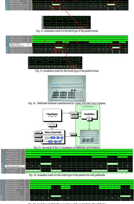
We used the Pathfinder, a small scale low cost hardware system with size of a notebook, developed by GFEC, Taiwan as shown in Fig. 14 in the hardware simulation of our designed system. The Pathfinder has a built-in Stratrix EP1S30 FPGA system, it can simulate around 470000 ASIC logic gates and it possess 7.4 Mbits embedded RAM. The Pathfinder is a low cost system comparing with the simulation system or the large scale prototype system it has been considered as the test platform for IC industry.
QuartusII and to the logic circuit of the circuit layer. The ModelSim then uses the Wrapper file, generated from MarpMarker, to generate the Testbench by adding the signals to be tested, it then combines with the synthesized circuit generated from Quartus II and this combined signal is downloaded and written into Pathfinder. The baseband circuit will be written into the actual circuit through Stratix 30 of the Pathfinder and the Testbench will be through the Pathfinder to synthesize the actual signal and to be used to test the operation of the circuit; finally the signal passes through the circuit will be transmitted back to ModelSim to validate the operation of the transmission system through the operation of the circuit.
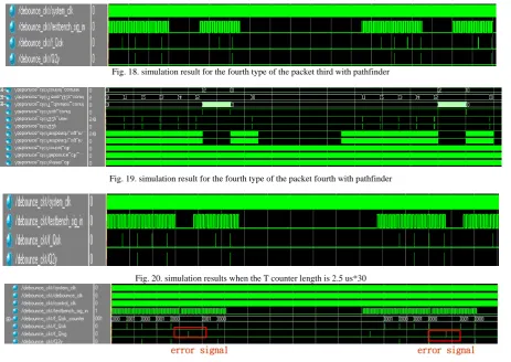
Finally the designed transceiver is written into the Pathfinder to validate its results. As shown in Fig. 16 is the simulation result for the first type of the packet signal it has exactly the same result as shown in Fig.10. For the test of type 2 packet signals it has the results as shown in Fig. 17, it is exactly the same as the result shown in Fig. 11. Similarly for the tests of type 3 and type 4 packets they have the test results as shown in Figs. 18 and 19 respectively, they are matched the results as shown before in Fig. 12 and 13 respectively.
A. Noise Simulation
When the transmitted 40 kHz is changed to 100 kHz or to 5 kHz they have the simulation results as shown in Figs. 10 and 11 respectively, they prove that if the system has an input signal with frequency not as the designed 40 kHz then the system will have no output signals. With interference signals it has the simulation results as shown in Figs. 12, 13, 16 and 17. The result in Fig. 14 is the Pathfinder hardware manufactured by Galaxy Far East Corp Company and Fig. 15 is the result of the Co-Emulation of Pathfinder and ModelSim, it appears that all interfering signals with frequency below 35 kHz and above 50 kHz have been filtered by the designed system [4][5].
B. Simulation of the Counter
As shown in Figs. 18, 19 and 20 are the simulation results when the T counter length is 2.5 us*30, 2.5us*20 and 2.5us * 15 respectively, it will not occur any mis-detection situations. But as shown in Fig.21 when the T counter length becomes 2.5 us * 10 it occurs mis-dections, this is because the separation between A session and C session is not far enough to have the detection working properly [6].
IV. CONCLUSION
In this paper we designed a transmission system with 200 kHz timing pulse and the packet information was transmitted at low power and low carrier frequency at 40 kHz. The system
description language and the ModelSim software program and was fabricated in the FPGA platform. These system characteristics can be further studied if noise effect is included in the system and some sort of non-synchronization existing between the transmitter and receiver terminals.
ACKNOWLEDGMENT
This study is partially support from the National Science Council, ROC under contracts NSC 100-2221-E-032 -031 –
REFERENCES
[1] Stenumgaard, P.F., “A simple impulsiveness correction factor for control of electromagnetic interference in dynamic wireless applications”, communications letters, Vol.10, pp. 147-149, 2006
[2] Yamanaka, M. Sampei, S. Morinaga, N., “Interference suppression with adaptive multipath control technique for broadband private wireless access systems”,
Electronics letters, Vol. 42, pp. 864-866 2006
[3] St. Jean, C.A. Jabbari, B., “On Wireless Game-Theoretic Power Control with Successive Interference Cancellation”, vehicular technology conference, pp.1-5, Sept. 2006
[4] Leung, K.K. , “Power control by interference prediction for broadband wireless packet networks”, wireless communications, IEEE transactions on, Vol. 1, pp. 256-265, April 2002
[5] Bartlett, V.A., Grass, E., “Exploiting data-dependencies in ultra low-power DSP circuits “, IEE seminar on, pp. 1-6, Jan. 2001
[6] Arslan, T., Ozdemir, E., Bright, M.S., Horrocks, D.H., “Genetic synthesis techniques for low-power digital signal processing circuits”, IEE seminar on, pp. 1-5, Feb. 1996
[7] Stenumgaard, P.F., “A simple impulsiveness correction factor for control of electromagnetic interference in dynamic wireless applications”, communications letters, Vol.10, pp. 147-149, 2006
[8] Yamanaka, M. Sampei, S. Morinaga, N., “Interference suppression with adaptive multipath control technique for broadband private wireless access systems”,
Electronics letters, Vol. 42, pp. 864-866 2006
[9] St. Jean, C.A. Jabbari, B., “On Wireless Game-Theoretic Power Control with Successive Interference Cancellation”, vehicular technology conference, pp.1-5, Sept. 2006
[10] Leung, K.K. , “Power control by interference prediction for broadband wireless packet networks”, wireless communications, IEEE transactions on, Vol. 1, pp. 256-265, April 2002
[11] Bartlett, V.A., Grass, E., “Exploiting data-dependencies in ultra low-power DSP circuits “, IEE seminar on, pp. 1-6, Jan. 2001
[image:3.595.49.559.184.549.2][12] Arslan, T., Ozdemir, E., Bright, M.S., Horrocks, D.H., “Genetic synthesis techniques for low-power digital signal processing circuits”, IEE seminar on, pp. 1-5, Feb. 1996
Fig. 2. Receiver
Fig. 5. basic packet format
Fig. 6. first type of packet format
Fig. 7. second type of packet format
Fig. 8. third type of packet format
Fig. 9. fourth type of packet format
A B C D
Fig. 10. simulation result for the first type of the packet format
[image:5.595.60.533.39.716.2]A B C D
A B C D
Fig. 12. simulation result for the third type of the packet format
[image:6.595.91.507.52.310.2]A B C D
Fig. 13. simulation result for the fourth type of the packet format
Fig. 14. Pathfinder hardware manufactured by Galaxy Far East Corp Company
MapMaker Pin Assignments
Altera QuartusII
(Proposed test system design)
TCL Script
ModelSim
P.L.I./ EDT Wrapper file
Test Bench
Download Synthesis
Place&Route
Probe&Debug
Co-Emulation
Mapper (pilot insertion) IFFT CyclicAdd
Prefix
Remove Cyclic Prefix FFT DeMapper (pilot remove)
PN sequence Generator Output
Data
Fig. 15. the result of the Co-Emulation of Pathfinder and Modelsim
[image:6.595.78.518.75.742.2]Fig. 18. simulation result for the fourth type of the packet third with pathfinder
Fig. 19. simulation result for the fourth type of the packet fourth with pathfinder
Fig. 20. simulation results when the T counter length is 2.5 us*30