CHAPTER 1
SPIN TRANSFER TORQUE: A
MULTISCALE PICTURE
Yunkun Xie1, Ivan Rungger 2, Kamaram Munira3, Maria Tsoneva Stamenova2, Stefano Sanvito 3, and Avik W. Ghosh1
1
Charles L Brown School of Electrical and Computer Engineering, University of Virginia, Charlottesville, VA
2School of Physics, AMBER and CRANN Institute, Trinity College, Dublin 2, Ireland 3Center for Materials for Information Technology, University of Alabama, Tuscaloosa AL
1.1 Introduction
1.1.1 Background
Due to challenges related to physical and electrical scaling, metal-oxide-semiconductor field-effect transistor (MOSFET)-based memory technology is now suffering from increased power leakage and endurance problems. For instance, static random access memory (SRAM) and dynamic random access memory (DRAM) are both volatile, and cannot maintain data when the supplied power is turned off. SRAM has a rel-atively high cost and the involvement of six transistors makes it unsuitable for high density integration. DRAM can sustain a very high density but suffers from energy dissipation due to the need to refresh its charge. Replacing volatile memory with non-volatile can eliminate standby power consumption and alleviate some of these problems. A universal memory that fills gaps in the contemporary hierarchy presents
title, edition.
By author Copyright c2014 John Wiley & Sons, Inc.
a powerful driving force behind the development of fast, high density, non-volatile memory technology.
Magnetic systems are promising candidates for next generation memory due to their intrinsic non-volatility and low dissipation during switching [1]. Two good examples of commercial magnetic storage systems are Hard Disk Drives (HDD) and magnetic random access memories (MRAM). In these systems, information is stored in the magnetization direction of nanometer sized magnets, while the switch-ing/writing process is driven by an external magnetic field. In HDD the separation of the read/write head from the storage units allows high density integration of nano-magnets, but the data can only be accessed sequentially. In contrast a MRAM has built-in wires in each memory cell that can generate magnetic fields to switch a mag-net at any address. Although these technologies are relatively mature, fundamental scalability issues exist with field switching [2]. The magnetic field is generated by passing a current through a wire, making it hard to scale and creating a large dissi-pative overhead which dominates the energy cost, even though the switching itself is energy efficient. The extra wires in memory cells also complicate the circuit and raise added concerns on the interference between different cells due to the non-local nature of magnetic field [3].
Spin transfer torque magnetic random access memory (STT-MRAM) offers a novel magnetic memory technology that overcomes some of those difficulties. In-stead of field switching, STT-MRAM switches a magnet with a spin-polarized elec-tric current through the so-called spin transfer torque effect (STT). This effect de-scribes the transfer of angular momentum from electrons spin polarized by a fixed magnet and delivered in the form of a torque to flip the magnetization of a free magnetic layer. The use of spin-polarized currents instead of a magnetic field of-fers a scalable solution for magnetic non-volatile memory. The ultimate goal for STT-MRAM is to replace or at least complement DRAM and/or SRAM to serve as a non-volatile memory in complementary metal oxide semiconductor (CMOS) cir-cuitry. This, of course, requires STT-MRAM to meet all the criteria for conventional memory, such as fast speed, high endurance and low error. Fortunately, STT-MRAM inherits the advantages of MRAM in terms of fast switching (< 10 ns close to SRAM and better than DRAM), very high endurance and non-volatility[4]. The employment of a current switching scheme allows for lower dissipation and high density. The continuous scaling of STT-MRAM has achieved higher density than SRAM and is expected to beat DRAM at the 20 nm technology node in the near future [2].
As promising as STT-MRAM seems, it is not a low power device. In order to switch a magnet with an acceptable endurance, the current density needs to be of the order of1010
−1011A/m2
ma-INTRODUCTION 3
terial and the magnetization of a ferromagnet, provides control on one another [8]. Over the last decade, a wealth of mechanisms have been proposed as ways to ro-tate a magnet, ranging from giant spin hall effect (GSHE)[9], thermal torque[10], and strain induced torque[11]. However, robust ultra-low energy magnetic switching still remains an open topic of research.
The application of STT has in the meantime ventured beyond memory. For in-stance, spin torque oscillators (STO) makes use of STT induced magnetization pre-cession to generated microwave signals from a nanometer scale magnet [12]. STO based networks have been designed to perform complex functions such as pattern recognition [13]. On the other hand, All spin logic (ASL) uses spin for low power computation. The idea in ASL is to avoid spin-charge signal conversion, simplifying the circuit and minimizing energy dissipation [14].
1.1.2 STT modeling: An Integrated approach
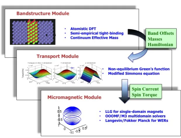
In the following sections we will discuss the development of computational tools as well as a broad physical understanding of STT-MRAMs, spanning different mate-rials and device geometries. This will culminate with a multiscale, integrated ap-proach (fig1.1). Given the description of the bandstructure of the magnetic tunnel junction, the transport module is used to calculate the current and the spin torque exerted on the free layer. The calculated spin torque is then fed into the stochastic macrodynamic module which can calculate the changing magnetization of the free layer. The band structure of the tunnel junction can be specified in 3 ways: a fully atomistic model(section 1.3), a parameterized model using continuum grid (section 1.3.2), and a quasi-analytical physics based compact model (section 1.2.1.1). The spin torque exerted on the free magnetic layer can be calculated at two levels of complexity: Non-Equilibrium Green’s Function (NEGF) combined with atomistic density functional theory (DFT) or with the parameterized continuum grid band-structure (section 1.3.2), and a modified Simmons’ equation for the quasi-analytical physics based compact model (section 1.2.1.2). Finally, the calculated torque from the transport module is included in the micromagnetic module to calculate the mag-netization dynamics in the free layer (section 1.4). The end result is a path from material properties to circuit metrics such as read write errors (e.g. fig 1.24).
Figure 1.1 Schematic diagram for the integrated approach.
From the point of view of device performance, there are three key metrics that we care about: energy dissipation, switching delay and read/write error. Different crite-ria apply to each, depending on the particular application. In general, an ideal device should be fast, energy efficient and have a low error rate. However, implementing all three requirements usually requires a subtle trade off among the underlying ma-terial and device parameters. For example in STT-MRAM the write error rate can be reduced by increasing the switching current or switching time, but the energy dissipation/speed are compromised as a result. Thus, a simultaneous analysis of the energy delay reliability tradeoff is essential[16].
THE PHYSICS OF SPIN TRANSFER TORQUE 5
Landau-Lifshitz-Gilbert (LLG) equation for the time evolution of the magnetization, or equivalently the Fokker Planck equation for its probability distribution. Analyti-cal and numeriAnalyti-cal results are presented for the switching delay and write error rate arising from stagnation points in the potential landscape. At the end we show how the separate parts can be combined to give a complete description of STT switching in MTJ, with examples all the way from material to device performance.
1.2 The physics of spin transfer torque
A typical STT-MRAM consists of a magnetic tunnel junction (MTJ) where all im-portant functions arise from the interplay between two ferromagnetic (FM) layers separated by a non-magnetic spacer (Fig 1.2). The FM layers have an intrinsic mag-netocrystalline anisotropy that is dependent on the magnetic material used and a demagnetization field which is dependent on the shape of the FM layer. The above two factors result in the FM layer having two bistable states. There can be an addi-tional interface anisotropy between spacer and FM layer[15, 17] that contributes to the overall energy landscape of the free layer. Depending on the orientation its easy axis, the magnetization can be ’in-plane’ (easy axis parallel to the junction plane) or ’perpendicular’ (easy axis perpendicular to the junction). One of FM layers has fixed magnetization while the other FM is free to rotate its magnetization. Two stable configurations can be established accordingly: FMs with parallel magnetization (P state) or anti-parallel (AP state). One bit information can thereby be encoded into the bi-stable states of MTJ.
The read and write operations are conducted by passing an electric current through the MTJ. For reading, a small voltage is applied across the spacer, causing electrons to tunnel between the FM layers. Inside the FM there exists an internal exchange field that breaks spin degeneracy and shifts the majority-spin, up, electronic states with respect to the minority-spin, down, states (Fig 1.2). Because of the different up and down spin densities of states at the Fermi energy, the electron current through the MTJ becomes different for P and AP configurations, with usually P showing a lower resistance because of the large overlap in states between the magnets, and AP showing a higher resistance because of the reduction in overlap. In other words, the tunneling currentJ(θ)and the resistanceR(θ)depend explicitly on the angular orientationθbetween the two contact magnetizations. The magneto-resistance ratio TMR:= (Rap−Rp)/Rphas been used to characterize the difference in tunneling resistance between P and AP configuration. With symmetry filtering (discussed in the next section) the TMR ratio in an MTJ can theoretically rise up to more than 2000%[18] in a perfect MTJ junction, with over200%observed experimentally at room temperature [19]. Such a high TMR is important for differentiating the P/AP configurations, allowing for a lower read current.
MTJs. At finite bias, the current gets polarized by the fixed magnet and thus carries angular momentum from one magnet to another. In a spin valve with non-collinear magnetizations, the misalignment between incoming spin and the local magnetic moment induces a torque on both the spins and the magnetization through exchange coupling. In the absence of spin-orbit coupling, this mutual interaction conserves total angular momentum, generating a torque equal to the divergence of the spin current within a given volume (see fig 1.16). This torque ultimately switches the free layer when it exceeds the threshold to overcome the restoring damping forces.
1.2.1 Free-electron model for magnetic tunnel junction
Much of the MTJ switching can be qualitatively understood in terms of a simple free electron model with a spin dependent barrier (Slonczewski, 1989[20]). By match-ing wave functions across the MTJ boundaries, we get an angle-dependent charge currentJ(θ), and thereafter express the TMR ratio in terms of the ’effective polar-ization’ for the MTJ stack. The spin torque, which is perpendicular to the free layer magnetization (the parallel component does not affect the dynamics, can be decom-posed into two orthogonal axes as(M~free×M~fixed)andM~free×(M~free×M~fixed). These two components will be shown to have completely different symmetries and voltage dependences. In the limit of the magnet being a half-metal (100%spin-polarization), the torques become symmetric and the P-AP/AP-P switching becomes identical.
1.2.1.1 Current and tunnel magnetoresistance Consider a magnetic tunnel junc-tion. In the free-electron approximation, the longitudinal part of the spin-polarized electron Hamiltonian across the MTJ can be written as:
H =~
2k2 ⊥
2m −
1 2
~
∆·~σ, x <0 or x > d (FM contacts)
H =~
2k2 ⊥
2m∗ +U(x), 0≤x≤d (oxide)
(1.1)
wheremandm∗are the effective masses in the ferromagnets and the barrier respec-tively,∆~ is the exchange field and~σ = (σx, σy, σz)are the Pauli matrices. If we choose the local z axis to be along the magnetization direction, the energy disper-sions of the longitudinal part for two spin channels are two parabolic bands shifted with respect to each other, as shown in fig 1.2. In the following we will simply write
k⊥,↑, k⊥,↓ask↑, k↓.
The magnetic tunnel junction can be broken up into three regions (Fig 1.2): (I)
x <0: the left ferromagnetic layer where the magnetization is pinned to the +z axis, (II)0≤x≤d: the insulating tunnel barrier and (III)x > d: the right ferromagnetic layer whose magnetization is free to rotate and is defined by the angleθmeasured with respect to the positive +z axis. The magnetization of the right ferromagnet is parallel to the z’ axis of the coordinate system x’,y’,z’, which is rotated atθdegrees to the original z axis. For simplicity, we first omit the transverse momentumk||and
THE PHYSICS OF SPIN TRANSFER TORQUE 7
𝐸
𝐹𝐸
𝐹 𝑒𝑉 𝑈 𝑋 𝑋 𝑍 𝑍 𝑋 𝜃 0 𝑑Δ
𝐸
𝐹1𝐸
𝐹2Region I Region II Region III
𝐸(𝑘)
𝑘
⊥↓ [image:7.595.102.386.128.219.2]𝑘
⊥↑Figure 1.2 Simple barrier model for magnetic tunnel junction. (Left). The band structure of the ferromagnetic contact. The bottom of↑and↓conduction bands in ferromagnetic(FM) contacts are separated by∆. EF is the Fermi energy. If EF = EF1 both spin-up and spin-down channels have non-zero density of states around the Fermi level. IfEF =EF2 only spin-up electron exists at the Fermi level and the FM is100%polarized. (Riight). When a bias is applied on the MTJ, the insulating barrier has a linear ramp potential.dis the width of the insulating barrier and U is is the barrier offset between the contact and the insulator. The magnetization of the right contact is rotated for an angleθfrom the magnetization of the left contact.
as:
Region I:ψ↑= q1 kl
↑
eikl↑x+R ↑e−ik
l
↑x
ψ↓ =R↓e−ik
l
↓x
Region II:ψσ= √ 1 κ(Ex,x)
Aσe−Eb(x)+BσeEb(x) Region III:ψσ0 =Cσeik
r
σx σ=↑,↓
(1.2)
The longitudinal spin-polarized electron momentum in each of the three region can be expressed as
Region I:kl↑=1 ~
√
2mE, k↓l = 1 ~
p
2m(E−∆)
Region II:κ(E, x) = 1 ~
p
2m∗[U−eV x/d−E],
Eb(x) =
Z x
0
κ(E, x0)dx0
Region III:kr↑= 1 ~
p
2m(E+eV), kr↓= 1 ~
p
2m(E−∆ +eV)
(1.3)
Notice that the wave function in region III,ψ↑0 andψ0↓, is written with respect to the local axes, x’,y’,z’. In order to conform to the original axes, a spinor transformation is required,
ψ↑=cos(θ2)ψ 0 ↑+sin(
θ 2)ψ
0 ↓ ψ↓=−sin(θ2)ψ↑0 +cos(θ2)ψ
0 ↓
(1.4)
Je= e~ 2m∗i
"
ψ∗↑ ψ↓∗ dψ↑/dx
dψ↓/dx
!
−(ψ↑ ψ↓) dψ∗
↑/dx dψ↓∗/dx
!#
(1.5)
Since the charge current is conserved throughout the junction, the equation can be evaluated at any point. Solving for the charge current to the leading order in
e−Eb(d)[21], we get
Je(E) =J0(1 +P2cosθ) (1.6)
where
J0(E) =
8e~κLκR m∗
(κ2
L+k↑lkl↓)(k↑l+kl↓)
(κ2 L+k↑l
2
)(κ2 L+k↓l
2
) (κ2
R+k↑rk↓r)(kr↑+kr↓)
(κ2 R+k↑r
2
)(κ2 R+k↓r
2
)e
−2Eb(d) (1.7)
P(E)2=(κ
2 L−k
l
↑kl↓)(kl↑−kl↓)
(κ2 L+k
l ↑k
l ↓)(k
l ↑+k
l ↓)
·(κ
2 R−k
r
↑k↓r)(kr↑−kr↓)
(κ2
R+k↑rk↓r)(kr↑+kr↓)
=Pl(κL, kl↑, k l
↓)Pr(κR, kr↑, k r ↓)
(1.8)
Pi = (κ2i −k i ↑k
i ↓)(k
i ↑−k
i ↓)(κ
2 i +k
i ↑k
i ↓)−1(k
i ↑+k
i
↓)−1, (i =l, r)are defined as
’effective polarization’ by Slonczewski because it is the product of the FM contact polarization(k↑i −k↓i)(k↑i+k↓i)−1and the coupling between the spacer and the FM contact,(κ2i−k↑ik↓i)(κ2i+k↑iki↓)−1. In order to obtain the total charge current through the MTJ, one needs to sum over the transverse momentum and integrate over energy. The TMR ratio can be related to the effective polarization:
TMR=IP−IAP
IAP ∝
2PLPR 1−PLPR
(1.9)
Note that this is the same formula as the famous Julliere model, except for the in-terpretation of polarization: Julliere model is rather ambiguous on the definition of spin-polarization (many people interpret it as the spin polarization of the bulk), while Slonczewski model incorporates the coupling between contacts and the barrier.
1.2.1.2 Spin current and torque The spin current is calculated as
Jσ(E) = e~
2m∗i
"
(ψ∗↑ ψ↓∗)σ dψ↑/dx dψ↓/dx
!
−(ψ↑ ψ↓)σ
dψ↑∗/dx
dψ↓∗/dx
!#
(1.10)
The spin current is not conserved inside the ferromagnetic contacts because of the presence of the internal exchange field. We therefore evaluate it atx= 0+ within
THE PHYSICS OF SPIN TRANSFER TORQUE 9
When the spin current goes from region I to region III, it deposits angular mo-mentum on the right ferromagnet that can switch from the AP to the P configuration. In the meantime, the first region also experiences a torque symmetrically induced by the transverse spin currents due to the removal of angular momentum (however being a fixed layer it stays pinned). This torque is analogous to the one we use for P-to-AP switching, when a negative voltage is applied and angular momentum is removed from the free layer. We will work out below the expressions for the two torques, which we will invoke later on to explain the asymmetry in the switching processes. When electrons are injected from I to III, the torques imposed on regions I and III work out to be
Region I:
τx,II→III(E) = e~
2m∗J0PRsinθ τy,II→III(E) =−4e
2
~2 m∗2 =
∆Rl
<[∆Rr] sinθe−2Eb(d)
(1.11)
Region III:
τx,IIII→III(E) = e~
2m∗J0PLsinθ τy,IIII→III(E) =
4e2
~2 m∗2 =
∆Rl<[∆Rr] sinθe−2Eb(d)
(1.12)
where=and<respectively denote the imaginary and real parts. Here ∆Rl,r = (Rl,r↑ −Rl,r↓ )/2is the difference in reflection coefficient for spin up/down electrons between the non-magnetic barrier and the FM contact. In this free-electron model, the reflection coefficient isR↑l,r,↓= (iκ−kl,r↑,↓)/(iκ+kl,r↑,↓).
For electrons injected from region III to region I, the spin transfer torque can be easily written out by making the changes (l↔r, θ↔ −θ) in the above equations. We will see the importance of these four torque expressions later in the chapter.
Region I:
τx,IIII→I(E) =τx,IIII→III(E)(l↔r, θ→ −θ)
τy,IIII→I(E) =τy,IIII→III(E)(l↔r, θ→ −θ)
(1.13)
Region III:
τx,IIIIII→I(E) =τx,II→III(E)(l↔r, θ→ −θ)
τy,IIIIII→I(E) =τx,II→III(E)(l↔r, θ→ −θ)
(1.14)
The total torque can be evaluated by integrating over energy (assume zero tempera-ture for simplicity)
τy(V) =
X
~ k||
Z ∞
Ec
(τy,IIII→III+τy,IIIIII→I)dE
=4e
2 ~2 m∗2 X ~k || " Z Ef L
Ec
sinθe−2E(d)=[∆Rr]<[∆Rl]dE
+
Z Ef R
Ec
sinθe−2E(d)=[∆Rl]<[∆Rr]dE
#
(1.15)
withEc being the bottom of the conduction band. Notice thatτy(V)is an even function ofV,τy(V) =τy(−V), if the two ferromagnetic contacts are made from the same material. Taylor expandingτy(V)as a function of bias, we get
τy(V)≈τy(0) + 1 2
∂2τ y ∂V2V
2
+o(V4) +. . . (1.16) At low voltage the y component varies quadratically withV and is non-zero even at zero bias, representing the exchange coupling between the two FMs [22]. In other words, the magnets want to orient in parallel/antiparallel (depending on the sign of
τy, i.e., whether the exchange parameter is ferro or antiferromagnetic), regardless of the sign of the applied bias.
τy(0) = 4e2
~2 m∗2
X
~k ||
Z Ef
Ec
sinθe−2E(d)=[∆Rl∆Rr]dE
≈ ~
2κ2e2
2π2m∗2d2sinθe −2κd
=[∆Rl∆Rr]
(1.17)
In contrast, when evaluating the x componentτx(V)(the current driven Slonczewski torque∝M~free×(M~free×M~fixed)), we getτx,IIII→III =−τx,IIIIII→I. The total torque can be evaluated as
τx(V) =
X
~k||
Z ∞
Ec
(τx,IIII→III+τx,IIIIII→I)dE
=X
~k||
Z Ef+eV /2
Ef−eV /2
τx,IIII→III(E)dE
∝ J0(Ef)PL(Ef) sinθV at low bias
(1.18)
The above equation shows that the current driven torque has a linear variation withV
THE PHYSICS OF SPIN TRANSFER TORQUE 11
1.2.1.4 Symmetry in P-to-AP/AP-to-P switching In experiments one observes different switching currents for P-to-AP vs AP-to-P. This difference is often at-tributed to two different processes involved, with the former arising from majority electrons added to the fixed layer, while the latter arising from minority carriers in-jected from the free layer and reflected back at the fixed layer/spacer interface to induce P-to-AP switching. This picture is unnecessarily confusing. It would indicate that a fully polarized free layer will have no minority carriers to inject and should not switch P-to-AP (in reality, it switches easier). It would also suggest that increasing the barrier thickness would quickly eliminate the P-to-AP process as the minority carriers must travel through two lengths of the oxide giving twice the tunneling in-duced decay constante−4Eb.In reality, the P-to-AP switching is driven not so much
by the addition of reflected minority carrier angular momentum, but instead by the removal of majority carrier angular momentum. The two processes are operationally ’symmetric’ in a sense that in both cases it is the majority carriers (their addition or removal) that determine the free layer switching. In section 1.4 through real-time magnetization dynamics simulation we will show that once the density of minority spin approaches the majority spin density the switching starts to happen, both for AP-to-P and P-to-AP switching. We will then demonstrate that for a half-metallic contact the P-to-AP switching process is not inhibited by the lack of minority carri-ers, but instead becomes equally efficient.
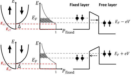
The observed asymmetry in switching current arises not from the simple differ-ence in majority and minority carrier density of states, but from their energy de-pendent polarization [21, 24, 25, 26]. To simplify the discussion we assume zero temperature and just look at the electrons injected around the fermi energy (see fig 1.3). The key point is that the torques for the two opposite cases are exerted by spins added to or removed from the fixed layer, involving filled states vs empty states in the two cases that sit at different energies (below vs above the fixed layer Fermi energy). Specifically, when a MTJ switches from AP to P, the polarized electrons are moved from the filled states in the fixed layer lying in the bias window betweenEF and EF−eV. From equations 1.11-1.12 we know the torque on the free layer is propor-tional to the polarization of the fixed layer, which is higher for these low energy states of the fixed layer. For P to AP switching, majority spins are removed from the free layer into the fixed layer empty states sitting betweenEF andEF+eV at a lower polarization. Since the effective torque on the free layer is proportional to the polar-ization of the fixed layer, we obtain an asymmetric torque (|τx(V)| 6=|τx(−V)|).
In the half-metallic limit (see fig 1.2 whenEF = EF2) electrons are 100%
po-larized around the fermi energy withk↓l =ipl, k↓r =ipr. The previous result for torqueτxon both Region I and Region III can be simplified and found to be the same (see eq 1.19). The equality is understood by the fact that the polarization is constant so thatτxis symmetric between positive and negative bias from previous discussion.
τx,II→III=τx,IIII→III =4e
2
~2 m∗2
κLκRkl↑kr↑
(κ2L+k↑l2)(κ2R+kr↑2)
𝐸𝐹− 𝑒𝑉
Δ
𝐸𝐹+ 𝑒𝑉
Δ
𝐸
𝐹𝐸
𝑃
fixed𝐸
𝐹𝐸
𝑃
fixed 11
Fixed layer Free layer
𝐸
𝐸
𝑬𝒄↓ 𝑬𝒄↑
[image:12.595.104.383.135.295.2]𝑬𝒄↓ 𝑬𝒄↑
Figure 1.3 Asymmetric torques on the free layer during AP-to-P and P-to-AP switching. Top: AP-to-P switching. Electrons from the fixed layer deposit angular momentum on the free layer. τxis related to the polarization of the fixed layer fromEF−eV toEF. Bottom: P-to-AP switching: Electrons are taken away from the free layer with its angular momentum. The corresponding torque is related to the polarization of the fixed layer from energyEF to
EF +eV. The polarization of the fixed layer is determined by its density of states and is energy depedent whenEF is not in the gap of minority band.
Note that the y component (perpendicular torque)τy(V) =b(V)M~free×M~fixed, whereb(V)≈B0+B1V2is the bias dependency, also contributes to the asymmetry
in AP-to-P/P-to-AP switching in an in-plane MTJ. A positive value ofb(V)prefers the parallel configuration in the MTJ while a negative value prefers the anti-parallel configuration for in-plane free layers, as we see in our micro-magnetic simulations (Fig. 1.4). The switching behavior can be easily understood from the approximate analytical solution to the micro-magnetic model (see section 1.4 for the definition of the parameters), where the critical switching current is modified by the perpendicular torque,
Ic−αB1=
1
η
2e
~
αµ0ΩHKMS(1 + MS 2HK
+ H
HK
) (1.20)
where H is the effective field due to perpendicular torque at zero voltage, H = (HK~ηB0)/(4qΩK), andB1is the additional perpendicular torque due to voltage
applied. The field like torque at zero voltage increases the thermal stability of the AP configuration and decreases the stability at the P configuration [23].
∆AP =
HKMSΩ 2KBT
1 + H
HK
2
∆P =
HKMSΩ 2KBT
1− H
HK
2
THE PHYSICS OF SPIN TRANSFER TORQUE 13
Figure 1.4 Simulation for AP to P switching in an in-plane magnetic layer. Magnetic properties of CoFeB,HK of 500Oe,MSof 1050 emu/cc andαof 0.02 are used. Positive perpendicular torque helps AP to P switching while a negative perpendicular torque delays the switching.
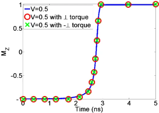
[image:13.595.100.361.405.591.2]In a perpendicular free layer, the field like torque only affects the precession of the magnetization and does not affect the switching speed (see Fig. 1.5).
1.3 ‘First principles’ evaluation of TMR and STT
The simple barrier model described in Section 1.2 captures the salient aspects of spin dependent transport. As we can see from Eq. (1.9) the TMR ratio increases as the polarization of the contact increases. However, the free-electron approximation is not always appropriate for real materials with complicated band structures. It is well known, for instance, that large TMR ratios can be achieved in epitaxially-grown crystalline Fe/MgO [27] and CoFeB/MgO [28] MTJs, reaching up to 604% at room temperature and 1144% at 5 K [29, 30] for CoFeB. These large TMR values are attributed to the phase coherent, transverse momentum conserving, transport arising from the energy, orbital and spin dependence of the tunneling matrices. Extensive re-views on the transport properties of crystalline MTJs can be found in Refs. [31] and [32]. In this section we will present a practical scheme for evaluating both the TMR and the STT of crystalline MgO-based MTJs from first principles. We will employ the NEGF approach [33] combined with DFT for the electronic structure descrip-tion. Our results are obtained with the SMEAGOLcode [34, 35], which constitutes a computationally-efficient (order-N) implementation of the NEGF+DFT method.
The ballistic current through the junction is calculated by using thetwo-spin-fluid approximation[36], where the spin-currents for majority (↑) and minority (↓) spins do not mix. In other words, we ignore spin-flip scattering. We assume periodic boundary conditions in the plane perpendicular to the transport and invoke Bloch’s theorem in plane. The total spin-dependent transmission coefficient,Tσ(E;V), for electrons at energy E is calculated self-consistently at an applied bias across the junction,V, and integrated to give the net spin current
Iσ(V) = e h
Z
dETσ(E;V)[fL−fR], (1.22)
whereσ={↑,↓}is the spin index andfL,Rare the bias separated Fermi functions of
the left and right electrodes, evaluated at(E−EF,L/R)/kBT (kBis the Boltzmann constant andT the temperature). The Fermi energy of the left electrode is given by
EF,L = EF +eV /2, and the one of the right electrode byEF,R = EF −eV /2, maintaining a zero average potential across the insulator (we can choose a differ-ent voltage convdiffer-ention as long as we consistdiffer-ently include the average drop in the insulator). HereEF is the Fermi energy of the semi-infinite electrodes atV = 0. Translational invariance in the transverse direction allows us to write
Tσ(E;V) = 1 Ωk
Z
dk⊥Tσ(E,k⊥;V), (1.23)
‘FIRST PRINCIPLES’ EVALUATION OF TMR AND STT 15
transmission coefficient for each transverse modek⊥as
Tσ(E,k⊥;V) = TrΓL,σ(E,k⊥)G†(E,k⊥)ΓR,σ(E,k⊥)G(E,k⊥). (1.24)
Omitting the spin and wave-vector arguments for simplicity, the retarded Green’s functionG(E)and the electrode-coupling matricesΓL,R(E)are defined as
G(E) =ES−H−ΣL(E)−ΣR(E)
−1
,
ΓL,R(E) =i
ΣL,R(E)−Σ†L,R(E)
,
(1.25)
whereHis the Kohn-Sham Hamiltonian matrix,Sis the overlap matrix, andΣL,R are self-energymatrices, which account for the presence of the two semi-infinite crystaline electrodes (leads) [33]. Tunnel junctions typically require largek⊥
sam-plings in order to convergeTσ(E;V). A100×100k⊥-point mesh is used for the
Fe/MgO/Fe junctions discussed in the following section.
1.3.1 The TMR effect in the MgO barrier
1.3.1.1 Symmetry filtering in Fe/MgO/Fe Calculations of the linear response cur-rent predict very large TMR for MgO based junctions [18, 37, 38, 39, 40, 41]. The TMR is found to be governed not only by the spin-polarization of the electrode DOS, but also by the details of wave function matching across the barrier. This is analyzed in detail in Ref. [18, 42], where it is shown that the decay of a wave function across the barrier depends mainly on two factors: 1) the specifick⊥-point in the 2D BZ
perpendicular to the transport direction (assumed alongz), and 2) the symmetry of the wave function. The bands in Fig. 1.6 summarize the underlying physics. In MgO, states with∆1symmetry at theΓ-point transform like a linear combination of
functions with1, zand3z2
−r2symmetry [18] and have no momentum components
in thex−yplane. These states share the symmetry of the conduction and valence band edges and thus their complex bands must bend around to connect them, making the corresponding decay constant particularly small when the Fermi energy lies at midgap. Furthermore, the lack of angular momentum components in thex−yplane maximizes their longitudinal energy and thus their decay lengths. In contrast, other midgap states such as∆5created out ofzxandzysymmetry, or∆2created out of x2−y2andxystates have much lower longitudinal energies for a given total energy, and do not share the symmetry of the conduction bands. Their complex bands do not need to bend around to connect with the two band edges, making them much less dispersive. We therefore have a strong symmetry filtering, where∆1 states decay
slowly across MgO but those with∆5,∆2and higher in plane angular momentum
components decay much faster.
In order to convert symmetry filtering into spin filtering, we need to align the MgO evanescent Fermi energy states with the propagating states in the contacts. For Fe, Co or CoFe electrodes, the hybridization between s-like and 3z2
−r2 states
Γ
H
H
Γ
X
MgO
Fe
Majority Spin Minority Spin complex band
(a) (b) (c) (d)
real band
0 5
-5
Mg
[image:16.595.94.394.124.406.2]Fe
O
Figure 1.6 (Top) The band origin of spin symmetry filtering. (a) LDA-based band structure and (b) complex band of bulk MgO. The∆1 complex evanescent band inside the bandgap of MgO turns around to connect the conduction and the valence band edges with which it shares an overall orbital symmetry. In contrast the∆5and∆02bands have significant angular momentum components perpendicular to the transport axis, so they do not share the band edge symmetry and, as a result, they are non dispersive and strongly decaying. Plotted alongside, (c) Fe enjoys a selective∆1majority spin band crossing the Fermi energy but (d) not one for the minority spin, converting the MgO symmetry filter into an Fe/MgO spin filter. (Bottom) From bulk to heterojunction (color online): unit cell used for the Fe/MgO/Fe(100) junction with 4 MgO MLs. Periodic boundary conditions are applied perpendicular to the stacking direction.
develops a propagatingΓ-point∆1band at the Fermi energy only for its majority
(↑) spins but not for the minority (Fig. 1.6), leading to a spin selective injection at the Fermi energy. The conjunction of energy placement, spin structure and orbital symmetry implies that Fe electrodes separated by a MgO barrier filter minority spins and effectively behave as half-metals. The corresponding TMR is expected to be very large [18, 37].
‘FIRST PRINCIPLES’ EVALUATION OF TMR AND STT 17
lattice parameter of 4.19 ˚A, which matches well the experimental value and also pre-viousab initiocalculations [46]. The generalised gradient approximation (GGA), in contrast, yields 4.29 ˚A, i.e. it slightly underbids. In Fig. 1.6 the LDA band structure is shown for the equilibrium lattice constant. We note that the band gap at theΓpoint is only 4.64 eV, which is about 3.2 eV smaller than experiments. This discrepancy is caused by the self-interaction error in the LDA exchange correlation potential, but does not change the qualitative features of the problem. Iron is a ferromagnetic metal and crystallizes in the bcc structure, with a room temperature lattice constant of 2.8665 ˚A [47, 48]. The agreement of the LDA band structure and DOS with the experimental ones is rather good [47, 49].
For bulk bcc Fe we obtain a relaxed lattice constant of 2.79 ˚A for LDA, and 2.88 ˚
A for GGA, which agrees well with other calculations [50]. The LDA band structure along theΓ-H direction is shown in Fig. 1.7a. This is also in good agreement with other LDA calculations [51] and with experiments [49]. All calculations presented in this section are performed at the LDA level, with the GGA results being rather similar. Minor differences are caused by differences around the Fermi level in the actual band structures obtained with LDA or GGA.
1.3.1.2 Interfacial configuration in Fe/MgO/Fe MTJ Although experimentally the Fe/MgO interface structure depends on the order in which the layers are grown, in all our calculations we use a completely symmetric Fe/MgO/Fe junction. Ac-cordingly, we assume that the Fe electrodes are fixed to their bulk lattice parameters (2.866 ˚A), while the in-plane MgO lattice adapts perfectly to Fe (lateral periodicity is enforced), making its lattice constant√2×2.866≈4.05A[55].˚
In Fig.1.6 we show the unit cell of a Fe/MgO/Fe(100) junction with a MgO bar-rier 4 monolayer (ML) thick. Periodic boundary conditions are applied in the plane perpendicular to the stacking direction. In all our transport calculations, based on the NEGF technique as implemented in the SMEAGOLcode, we use 8 Fe layers on each side of the MgO in order to converge to bulk. We construct MgO barriers with an ar-bitrary number of MLs by using 2.196 ˚A as the spacing between the MLs. Except for the first interface layer, it is assumed that the Mg and O atoms always have the same
zcoordinates [39]. A 7×7k⊥-points mesh is used during the self-consistent cycle
to converge the charge density, while a 100×100k⊥-point mesh is used over the full
BZ for evaluating the transmission coefficient in a single post-processing step. This finer mesh is necessary in order to resolve sharp resonances in the transmission. We use a real space mesh cutoff of 600 Ry and an electronic temperature of300K.
Γ H z -2
-1 0 1 2
E
-E
F
(e
V
)
10-4 10-2
T
(P)↑ ↓
10-4 10-2
T
(AP)0 1 2
n
c0 3 6
DOS
0DOS
3 6∆
1↑∆
1↓a)
b)
c)
d)
e)
(arb. units) (arb. units)
[image:18.595.76.401.119.321.2]f)
Figure 1.7 (a) Bulk Fe band-structure along theΓ → Hdirection (the bands with∆1 -symmetry are thickened), (b)Tσ in the P configuration, (c)Tσin the AP configuration, (d) average number of open channels perk⊥-point for bulk Fe, nc, (e) bulk Fe DOS and (f) interface Fe-layer DOS, all for both majority and minority spin (σ =↑,↓). Note that the ∆1 band-edges coincide approximately with a rather sharp increase in both transmission coefficientsT↑,↓. Figure reprinted from ref[55] with permission from the authors.
the Fe interface layer for both majority and minority spins. By definition,
N = 1
πΩBZ
Z
dk⊥
Nk(open)
⊥
X
i 1
vk⊥,i
and nc=Nv=
1
π
Z
dk⊥N (open)
k⊥ , (1.26)
where the integral runs over the 2D BZ perpendicular to the transport direction,
Nk(open)
⊥ is the number of open channels for a givenk⊥andvk⊥,iis the group veloc-ity for channeli.
For the MTJ P configuration, and for energies in the range of about±1eV around
EF, the transmission for ↑spins is much larger than that for the ↓spins (note the
logarithmic scale). Very close toEF, however, there is a sharp peak in the minority
transmission (T↓), which is due to an interface (IS) state found close toEF. Below
about -1 eV,T↑drops out as well as this is the energy of the band-edge of the majority
∆1state,∆↑1, at theΓpoint (see Fig. 1.7a). At this energy we also find a IS in the
↑ spins, which causes the peak in the transmission. The sharp increase in T↓ at
about 1 eV to 1.5 eV is due to the fact that at 1.5 eV there is the band-edge of the minority ∆1 states,∆↓1, at the Γ point. For other energies inside the MgO band
gap the transmission varies, following also the change in the number of channels. An increase innc usually is translated in an increased transmission. For energies
‘FIRST PRINCIPLES’ EVALUATION OF TMR AND STT 19
Tmax
Tmax
10−10
Tmax
4 ML
P majority
16 ML
24 ML
AP majority
10−5
[image:19.595.75.446.124.354.2]P minority
Figure 1.8 (color online)k⊥-resolved transmission coefficient atEFfor the↑and↓spins in the P configuration, and for the↑spins for the AP, for different MgO thicknesses. In each figure a different logarithmic color scale is used, where the red color corresponds to the maximum transmission of each figure,Tmax, and the blue color corresponds to10−10Tmax.
of channels, with the scattering across the MgO bands leading to some variations. As a first approximation, the transmission in the anti-parallel (AP) configuration can be seen as a convolution of the majority and minority transmission in the parallel one [52, 53]. AroundEFit is much lower than the one for the P configuration. The
resulting 0-bias TMR is very large, namely 1780%.
In Fig. 1.8 we show thek⊥-dependent transmission coefficient atEF, for↑(first
row) and↓(second row) spins in the P configuration, and↑spins in the AP, evaluated for 4, 16 and 24 MgO MLs. The color code is chosen in such a way that for each graph the red color corresponds to the relative maximum transmission. Therefore the red spots indicate in which parts of the BZ the transmission is large. The blue color is chosen to be10−10 times smaller than such maximum value. Hence, the main contributions to the transmission originate only fromk⊥-points close to Γ. TheΓ
point filtering effect is enhanced when the thickness of the MgO layer is increased.
dif-0
10
20
30
z
(Å)
-0.4
-0.2
0
0.2
∆
V
H(eV)
Fe
MgO
0
0.5
1
1.5
2
V
(V)
0
1
2
3
4
5
6
I
(A/
µ
m
2
)
P: SCFP: RSAAP: SCF AP: RSA
[image:20.595.87.397.132.256.2](a)
(b)
Figure 1.9 (a) Planar average∆VHof the difference between the self-consistent Hartree potential at 0.5 V and the one atV = 0(full line). The dashed line indicates∆VHapplied in the rigid shift approximation. Diamonds and dots indicate the location of the Fe and MgO layers, respectively. (b) Comparison of theI-V curves for the P and AP configurations obtained with the self-consistent solution (solid lines) and with the rigid shift approximation (dashed lines).
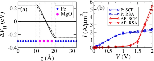
ference between the planar average of the self-consistent Hartree potential at finite bias (0.5 V) and that atV = 0along the junction stack (z-axis).∆VHdecays almost
linearly across MgO and it is flat in the electrodes. The dashed line indicates the ideal linear potential drop, which we refer to as therigid shift approximation (RSA). In the RSA the finite bias transmission coefficient is calculated self-consistently only atV = 0, and then modified under finite bias by applying a rigid shift to the elec-trode DOS and the electrochemical potentials, bridged by a linear ramp inside the MgO [40]. In order to isolate the effect of charging the junction on the transport we compare theI-V curve obtained fully self-consistently against the one obtained with the RSA, Fig. 1.9(b). We find that indeed theI-V is minimally affected by charging, making the rigid shift approximation reasonable for Fe/MgO junctions. It is clear from the currents in the P and AP configurations that the resulting TMR is expected to be high at low biases and then to decrease with bias.
The calculated TMR ratio as a function ofV is presented in Fig. 1.10(a), where one can notice a clear non-monotonic behaviour. Firstly, there is a very sharp de-crease of the TMR for a narrow voltage region around V = 0, followed by an increase. For large voltages the TMR decays monotonically, leading to a peak at aboutV = 0.3 V. The dependence of the TMR on the bias is determined by the
I-V characteristics of the P and AP configurations of the MTJ, which in turn can be understood by looking at the evolution of the various transmission coefficients as a function of bias. These quantities are presented in Fig. 1.11 and help us in driving the discussion.
Three main features characterise the evolution ofT(E;V)withV. These can be identified from the plot ofT(E;V = 0)for the P configuration as: 1) a sharp increase in transmission at around -1 eV for the↑spins, which is mainly determined by the electronic structure of Fe alone and in fact corresponds to the↑spins∆1band
‘FIRST PRINCIPLES’ EVALUATION OF TMR AND STT 21
10-4
10-2
T
-2 -1 0 1 2
E-E
F
(eV)
10-4
10-2
T
δ = 0 Ry
δ = 10-4 Ry
δ = 10-3 Ry
0 0.5 1 1.5 2
V
(V)
0 2000 4000 6000 8000
TMR (%)
0 0.1 0.2
V (V)
1000 2000
(a)
(b)
[image:21.595.83.396.132.281.2](c)
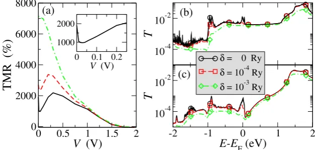
Figure 1.10 (a) TMR as a function of voltage,V. Hereδis an imaginary energy added to the Green’s function, which mimics the effects of scattering due to disorder. The black curve is forδ= 0, the red forδ= 10−4
Ry, and the green forδ= 10−3
Ry. In the inset the TMR is shown in the low-bias region forδ= 0.. T(E;V = 0)for different values ofδfor the P (b) and the AP (c) configuration. Figure reprinted from ref [55] with permission from the authors.
+1 eV for the↓spins (peak 2), which corresponds to the↓spins∆1band edge; 3)
a sharp resonance atEFfor the↓spins (peak 3), which is attributed to the presence
of a transport resonance across↓spins surface states localised at the two interfaces between Fe and MgO.
As a voltage is applied to the junction the minority resonance atEFfor the P
con-figuration splits into two much smaller peaks and the transmission drops drastically. This is because the surface state at the two sides of the junction drift in energy in opposite directions and the resonant condition is lost. Such resonant condition is not present for the AP configuration, since minority spins at one electrode tunnel into the majority ones at the opposite electrode and viceversa. It is such drastic reduction of the transmission in the minority channel of the P configuration that yields to the reduction in TMR at low bias. Note that such reduction occurs on a voltage scale of the order of 20 mV, which is comparable with the natural width of the surface states.
As the bias continues to increase the transmission for the P configuration becomes entirely dominated by the↑spin channel, for whichT(E;V)is constant in energy over the bias window. This produces a linearI-V curve, which saturates as soon as the∆1majority band edge enters the bias window. In contrast the transmission
for the AP configuration remains small in the bias window up to relatively large voltages. Then, for one of the two spin channels (in the AP case the spin channels are defined with respect to one of the two electrodes) the majority spin∆1 band
edge of one of the two electrodes starts to overlap in energy with the minority∆1
10-4 10-2
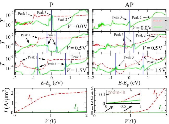
T
P
10-4 10-2T
-2 -1 0 1 2
E-EF(eV)
10-4 10-2
T
0 1 2
V (V) 0 1 2
I
(A/
µ
m
2)
AP
-2 -1 0 1 2
E-EF(eV)
↑ ↓
0 1 2
V (V) 01 2 3 4 5
0 0.5 1
0 0.1
V= 0.0V V= 0.0V
V= 0.5V
V= 1.5V V= 1.5V
V= 0.5V
I
↑I
↓I
↑I
↓ zoom-in Peak 1 Peak 2 Peak 3 Peak 1 Peak 2 Peak 3 Peak 1 Peak 3 Peak 2 Peak 3Peak 3 Peak 2
Peak 3
[image:22.595.78.403.127.364.2]Peak 2
Figure 1.11 Spin-dependent transmission coefficient,T(E;V), as a function of energy,E, and for different biases,V, for the P (left-hand side panels) and for the AP configuration (right hand side panels). The vertical lines are placed atE =EF±eV /2and enclose the bias window. Figure reprinted from ref [55] with permission from the authors.
In the analysis presented so far we have considered phase-coherent transport across a perfectly crystalline junction, a situation that typically does not correspond to an actual experiment [54]. Unstructured disorder can be introduced in the calcula-tion of the transmission coefficients by simply adding a small imaginary component
δto the energy when evaluating the Green’s function. The effect of such imaginary energy is that of broadening the resonances in the transmission, i.e. in reducing the life-time of the various surface states. This has the effect of smoothing the transmis-sion function as it can be appreciated in Fig. 1.10. The consequence on the TMR of such broadening depends on the details of the junction. In the case investigated here the low-bias non-monotonic dependence of the TMR ratio is washed away and atδ= 10−3Ry the TMR decreases monotonically across the entire bias range. No-tably the low-bias TMR is significantly larger for largeδ, while it is not sensitive to the broadening for large voltages, since in this case theI-V curve is dominated by the relative position of the∆1band edges and not by surface states. A monotonic
decay of the TMR bias is what commonly observed in experiments for high-quality junctions [27].
‘FIRST PRINCIPLES’ EVALUATION OF TMR AND STT 23
Figure 1.12 (color online) Isosurface of the local DOS of the VOdefect band (purple color); red spheres represent O atoms, and green spheres represent Mg atoms.
however, that oxidation of the interface Fe layers can lead to a drastic reduction of the TMR, which can even become negative for asymmetric oxidation of the electrodes [56, 40, 41, 57]. In Ref. [27] it is noted that lattice dislocations are found at the Fe/MgO interface. These also can lead to a reduction of the TMR. Another possible mechanism leading to a reduction of the TMR is the presence of defects in the MgO, and at the Fe/MgO interface. Calculations for a Fe/vacuum/Fe junction indicate that disorder at the interface can drastically reduce the TMR [58], in agreement with the results of Ref. [57] for a disordered and randomly oxidized Fe/MgO/Fe junction. Experimental results indicate that the density of defects in MgO depends on the growth conditions [59, 60, 61]. Such a large defect density is found to lead to an effectively reduced MgO band gap [60, 61]. In Ref. [60] it is shown that by annealing the sample the band gap opens to the bulk MgO value, indicating that the density of defects is reduced. Measurements of isolated defects indicate a defect level close to the valence band, which is tentatively attributed to Mg vacancies (VMg), and a set of
levels between theEFand the conduction band, attributed to oxygen vacancies (VO).
The authors note, however, that this correspondence is not completely established at this stage. In Ref. [61] a detailed study of the possible defects in MgO, grown on an Ag substrate have been presented. They find different possible defects, with energies spread over large part of the MgO band gap. One of the defects identified is VO, whose energy lies approximately in the middle of the MgO band gap. This
agrees well with other theoretical predictions [62, 63, 64].Ab initiocalculations with Fe/MgO/Fe junctions in Refs. [65, 66] show that for VOLDA predicts a defect band
centered about 1 eV below the Fe Fermi energy. In Ref. [67] experimental evidence is shown on the decrease of the TMR with VO, supported by a theoretical model.
1.3.1.5 Interfacial defects: Oxygen vacancy In order to investigate the bias de-pendent influence of defects on the transport, we perform calculations with a VO
inserted within MgO (Fig. 1.12). We find that such a defect has ans-type symme-try (consequently contributes to∆1 symmetry bands) and lies very close to the Fe
Fermi energy, in good agreement with the results of previous calculations [65, 66]. It is thus indicative of all defects that lead to a small additional DOS in the vicinity ofEF. The exact theoretical description of defects in MgO is a complex task; for
0.0 1.0 2.0 3.0 4.0 I (mA/ µ m 2 ) 0.0 1.0 2.0 3.0 4.0 I (mA/ µ m 2 ) 0.0 1.0 2.0 3.0 4.0 I (mA/ µ m 2 ) 0.0 1.0 2.0 3.0 4.0 I (mA/ µ m 2 ) 0.0 1.0 2.0 3.0 4.0 I (mA/ µ m 2 ) 0.0 1.0 2.0 3.0 4.0 I (mA/ µ m 2 )
0 0.5 1 1.5
V(V) 0.0 5.0 10.0 15.0 TMRr(10 3 %)
0 0.5 1 1.5
V(V) 0.0 5.0 10.0 15.0 TMRr(10 3 %)
0 0.5 1 1.5
V(V) 0.0 5.0 10.0 15.0 TMRr(10 3 %)
NorOrvacancy Orvacancyrinr4thlayer Orvacancyrinr2ndlayer
parallel
anti-parallel
[image:24.595.76.416.132.334.2]Total Spin up Spin down
Figure 1.13 Role of oxygen vacancy on tunnel magnetoresistance. The figure shows the spin-polarized current,I, for the P (top row of figures) and the AP alignment (middle row of figures) of the Fe electrodes, as well as the resulting TMR (bottom row of figures). In the plots for the current the red curves correspond to the↑current, the green curves the↓current, and the black curves to the total current. The results are for 8 MLs of MgO with no VO(leftmost panels), with a VOin the forth layer from the interface (middle panels), and with a VOin the second layer from the interface (rightmost panels).
defects can be described accurately with DFT. However, previous calculations show that DFT can accurately predict the properties of VO’s [62, 63, 64].
In order to keep the size of the calculations tractable, we use a rather high VO
density. We construct a2×2 supercell in the plane perpendicular to the transport direction. The VOis then obtained by removing one O atom in one of the MgO MLs.
The planar VOdensity is therefore 1/4, the total defect density for a 4 MLs junction
is 1/16, for a 8 MLs it is 1/32. In all the calculations in this section we do not relax the structure around the defect, and for the Fe/MgO junction we use the unrelaxed coordinates (Ref. [18]). We note that in our calculations the VOis in a charge neutral
state, whereas experimentally the vacancy can exist in different charging states. The presence of a VOleads to a defect band lying approximately in the middle of the gap
(not shown here). Importantly, this defect level is not spin-split. The band shows a rather large dispersion, which is due to the high in-plane defect density.
The bias dependence of the TMR is calculated for a defect-free and for two defec-tive 8 ML junctions: one where the VOis located in the second ML, and one where
‘FIRST PRINCIPLES’ EVALUATION OF TMR AND STT 25
10 10
−7 0
10−3
the 2
ndlayer
Oxygen vacancy in
No vacancy
AP
↓
[image:25.595.78.418.125.253.2]P
↑
P
↓
AP
↑
Figure 1.14 (color online)k⊥-dependent transmission for P↑(first column), P↓(second
column), AP↑(third column), and AP↓(fourth column), at an energyE−EF =−0.2eV. The first row of figures is for an ideal 8 MgO MLs junction, the second row is for a junction with a VOin the second MgO layer from the interface.
not lead to a significant change of the P current, although there are some quantita-tive differences with respect to the defect-free case. Overall we see that the TMR is drastically reduced in the junctions containing the VO’s, and basically vanishes if
the vacancy is at or closer to the interface than the second ML.
Clues for the enhanced AP transmission in the defective junctions can be found in thek⊥-dependent transmission presented in Fig. 1.14 for the ideal junction, and
for the 8 ML junction with the VOin the second ML. The plot showsT(k⊥)at an
energy of -0.2 eV belowEF. This is lower than the lowest energy of the surface state,
and lies in the region of high transmission for the AP configuration in the defective junctions. For the ideal junction the transmission is highest for the P↑states, since in that case there is a large density of the high-transmission∆1-like states on both
sides of the junction. For the P↓the contribution of the∆1like states on both sides
of the junction is rather small, and the transmission is correspondingly reduced. In the AP configuration the transmission is identical for↑and↓, as the perfect junction is completely symmetric. Since on one side there is a high density of∆1 states,
whereas on the other side the density is low, the transmission is much smaller than for P↑, but somewhat larger than for P↓.
For the junction with the VO in the second ML, the situation is very different.
Since the vacancy is not spin-polarized, the electrons flowing through the vacancy states at this energy have approximately the same density of∆1states for both↑and
↓. On the left side of the junction to which the VO is very close, there is a large
∆1 DOS for both↑ and↓. On the right side and for P configuration, the ↑has a
much larger contribution from the∆1states than the↓, so that the P↑transmission
that the enhancement in transmission in the AP configuration in a defective junction is caused by the depolarization of the∆1states at the vacancy site. If this sits very
close to the Fe/MgO interface, it effectively leads to a depolarization at the interface. If the vacancy lies in the middle of the junction, the effect is less pronounced, since the states need to tunnel to the vacancy site from both interfaces, where the∆1DOS
is small. However the TMR is reduced in this case as well. Ourab initioresult agrees qualitatively with the conclusions of Ref. [67].
1.3.2 Currents and torques in NEGF
After the extensive discussion on the TMR characterizing the read operation, let us now move on to the spin torque relevant for the write operation. As outlined in Sec. 1.2, the torque acting on a magnetic layer can be obtained by evaluating the difference in spin currents on the left and right of this layer. We formulate the general NEGF based formalism for evaluating such spin-currents in non-collinear systems from first principles. The NEGF Hamiltonian is obtained either from DFT or else from an empirical tight-binding (TB) model, projected over a localized orbitals basis set. The so obtained single particle Hamiltonian,H, and the density matrix,ρ, can be written as a sum of a spin-dependent part and spin-independent part
H =H0·I+H~S·~σ ρ=ρ0·I+ρ~S·~σ
(1.27)
where~σ = (σx, σy, σz), withσx, σy, σz the three Pauli matrices, andIis the 2×2 unity matrix.H0is the spin-independent part ofH, whileH~S= (Hx, Hy, Hz) rep-resents the spin-components ofHcorresponding to the exchange field. In the same wayρ0is split into its spin-independent partρ0and its spin-vector~ρS = (ρx, ρy, ρz). Note thatHαandρα, withα∈ {0, x, y, z}, areNo×Nomatrices, withNobeing
the number of orbitals in the simulation cell.
UsingG,ΓL,RandfL,Rintroduced in section 1.3, we can define the lesser Green’s
function,G<(E), as
G<(E) =iGΓLG†fL+iGΓRG†fR. (1.28)
Analogous toHandρwe can splitG<(E)into its spin components
G<(E) =G<0(E)·I+G~<S(E)·~σ, (1.29) withG~<S(E) = G<
x(E), G<y(E), G<z(E)
. The density matrix is then related to
G<(E)by
ρ= 1 2πi
Z ∞
−∞
G<(E)dE. (1.30)
‘FIRST PRINCIPLES’ EVALUATION OF TMR AND STT 27
the bond currentJij[68], and can be separated in its spin componentsJij(E) = Je,ij(E)·I+J~S,ij(E)·~σ, withJ~S,ij(E) = (Jx,ij(E), Jy,ij(E), Jz,ij(E)), and the energy dependent electron currentJe,ij(E). Within the NEGF formalism, and for systems with general overlap matrixS(of dimensionNo×No), the spin-dependent
bond current is given by
Je,ij(E) = 4e
h<
(H0,ij−ESij)G<0,ji(E) +Hx,ijG<x,ji(E) +Hy,ijG<y,ji(E) +Hz,ijG<z,ji(E)
Jα,ij(E) = 4e
h<
Hα,ijG<0,ji(E) + (H0,ij−ESij)G<α,ji(E)
,
(1.31)
withα∈ {x, y, z}, and<denotes the real part. The total spin current is obtained by integrating over all energies, and results to
Ie,ij =− 4e
~=
[H0,ijρ0,ji−SijF0,ji+Hx,ijρx,ji+Hy,ijρy,ji+Hz,ijρz,ji] Iα,ij =−
4e
~=
[Hα,ijρ0,ji+ (H0,ijρα,ji−SijFα,ji)],
(1.32)
withα∈ {x, y, z}, and=denotes the imaginary part. Here we have introduced the energy density matrix,F, which is given by[69]
F = 1
2πi
Z ∞
−∞
EG<(E)dE (1.33)
In order to obtain the current from a subsystem, denoted asSS1, to another
sub-system, denoted asSS2, one needs to sum over all the possible orbital-to-orbital
currents
Iα,SS1,SS2=
X
i∈SS1
X
j∈SS2
Iα,ij, (1.34)
withα ∈ {e, x, y, z}. In a layered system such as typical MTJs, we can evaluate the current across different layers. We denote asIα,nthe current across a layer with indexnin our cell, so thatSS1includes all orbitals with centers on or to the left of
layern, whileSS2includes all orbitals with centers to the righ of layern. As
0 10 20 30 40
layer number,
n
0 0.5 1
I
α,n
(10
10
A
m
-2
)
Totalα= x α= y α= z
[image:28.595.125.355.136.301.2]Fe MgO Fe
Figure 1.15 Layer-resolved spin current at 0.5 V for a Fe/MgO/Fe junction, with the layer index denoted byn(n∈[1,19]correspond to the Fe layers in the left electrode,n∈[20,25] are the MgO monolayers, andn∈[26,41]correspond to the Fe layers in the right electrode).
1.3.3 First principles results on spin transfer torque
Ab-initiocalculations of spin transfer torque habe been performed for various junctions[72, 73, 74]. We evaluate the STT for a the defect-free Fe/MgO/Fe tunnel junctions in-troduced in Sec. 1.3.1. Here we use 6 MgO monolayers, so that the interface state contribution to the current is suppressed. In Fig. 1.15 the layer resolved spin-current is shown for the different layers in our simulation cell. We apply the bias voltage non-selfconsistently within the RSA, since it gives a good approximation for the current when compared to the fully self-consistent solution (see Fig. 1.9). The bias voltage corresponds to 0.5 V, and the magnetic moment of the left electrode is along thez direction, while the one for the right electrode is along thexdirection. We see that the current is fully polarized alongz (x) deep in the left (right) electrode, showing that the local spin-current is parallel to the magnetization in the electrode. A torque is exerted at the layer indexnwhereIα,nchanges significantly. We see that the torque is localized mainly at the Fe/MgO interfaces. For example,Iz,ndrops from its left-electrode bulk value to approximately 0 within the first 4 Fe layers of the right electrode, which implies that the total torque alongz(the in-plane torque for the right electrode) acts within these first 4 Fe layers. The out-of plane torque is determined by theycomponents of the spin-current, and acts also mostly close to the MgO/Fe interfaces, although it protrudes deeper into the electrodes. Importantly, we note that the total electron current is constant over the whole system.
‘FIRST PRINCIPLES’ EVALUATION OF TMR AND STT 29
Fig. 1.17 shows the first principles torque. As discussed earlier, the low bias current driven STT is linear inV while the field like STT is quadratic inV, with a small non zero component even at equilibrium. This smallV = 0out-of-plane torque is due to the exchange interaction between the left and right Fe electrodes across the MgO. At high bias above∼1.5 V the torque shows a highly non-monotonic behavior and can also change sign. This is due to the fact that at these high voltages the current in the anti-parallel configuration increases rapidly and eventually becomes larger than the one for parallel alignment (see Fig. 1.13 for the 8 MgO monolayer junction).
MgO
FM1 (Fixed layer)
FM2 (Free layer)
𝑱
𝒔,𝒊𝒏𝑱
𝒔,𝒐𝒖𝒕≈ 𝑱
𝒛′𝝉 = −𝝁𝑩∫ 𝒅𝑽𝜵 ⋅ 𝑱 𝒔= 𝝁𝑩𝑨 𝑱 𝒔,𝒊𝒏− 𝑱 𝒔,𝒐𝒖𝒕
𝜏𝑥′ In − plane = 𝝁𝑩𝑨 𝑱 𝒙′,𝒊𝒏− 𝑱 𝒙′,𝒐𝒖𝒕 ≈ 𝝁𝑩𝑨𝑱 𝒙′,𝒊𝒏 𝜏𝑦′ Out − of − plane = 𝝁𝑩𝑨 𝑱 𝒚′,𝒊𝒏− 𝑱 𝒚′,𝒐𝒖𝒕 ≈ 𝝁𝑩𝑨𝑱 𝒚′,𝒊𝒏
A: the area of the junction
𝒁
Figure 1.16 Schematic of the definition of the STT at the right-hand-side electrode through spin-current fluxes.
In the literature the total electron density is often split into a ”condensate” or ”equilibrium part” (EP), and a ”non-equilibrium part” (NEP) [34]. Within NEGF the EP is usually written as
ρEP=
1 2πi
Z ∞
−∞
(−1) G(E)−G†(E)
[ξfR+ (1−ξ)fL]dE, (1.35)
and the NEP as
ρNEP=
1 2πi
Z ∞
−∞
iG(E) [ξΓL−(1−ξ)ΓR]G†(E) (fL−fR)dE, (1.36)
withξ∈[0,1], so thatρ=ρEP+ρNEP. Such a partitioning is not physically
moti-vated and the choice of the terms ‘equilibrium’ and ‘nonequilibrium’ is somewhat of a misnomer. The true ‘equilibrium part’ would correspond tofL =fRand the
-5 0 5 10 15
e
/(
µB
A
)
τ||
(10
10 Am
-2 )
Equilibrium Part
-2 -1 0 1 2
V (V)
-5 0 5 10 15
e
/(
µB
A
)
τ⊥
(10
10 Am
-2 )
ξ = 0
ξ = 1
Non-equilibrium Part
-2 -1 0 1 2
V (V)
Total
-2 -1 0 1 2
[image:30.595.94.390.129.360.2]V (V)
Figure 1.17 Bias dependence of the ‘equilibrium’ and ‘non-equilibrium’ components (defined in the text) of the in and out of plane components of STT for a Fe/MgO/Fe junction with 6 MgO monolayers, withξdefined in Eqs. (1.35) and (1.36).
just an energy window over which the residual NEP integral needs to be computed brute force. Sinceξcan be chosen arbitarily in the range from 0 to 1, the splitting in EP and NEP is not unique. In the same way the energy density is split into EP and NEP. The EP of the torque is then obtained by usingρEPandFEPin Eq. (1.32),
while the NEP torque is obtained by usingρNEPandFNEP, so that the total torque
is the sum of EP and NEP torques. The results are shown in Fig. 1.17 forξ= 0and
ξ= 1. While the in-plane torque is identical for any choice ofξ, it can be seen that the individual out-of-plane components change completely depending on the choice ofξ. Importantly, the total out-of-plane torque is independent of the choice ofξ, indicating thatthe only meaningful quantity is the total torque, and it is not really meaningful to split it into the arbitrary EP and NEP parts.
MAGNETIZATION DYNAMICS 31
−2 −1 0 1 2
Voltage (V)
Out−of−plane STT
−2 −1 0 1 2
−5 0 5 10 15
Voltage (V)
e/(
µ B
A)
τ
(10
10
Am
−2
)
In−plane STT
−0.4 −0.2 0 0.2 0.4
−0.4 −0.2 0 0.2
−0.4 −0.2 0 0.2 0.4
−1 0 1
[image:31.595.88.387.127.334.2]FeCo−MgO−CoFe CoFe−MgO−FeCo Co−MgO−Co Fe−MgO−Fe
Figure 1.18 Comparison of in-plane and out-of-plane STT for different electrode compositions.
junction we find the onset of the non-linear behavior for the in-plane torque already at about 1 V. The early onset of nonlinearity arises from the fact that Co has one more electron than Fe, so that the Fermi energy is effectively shifted to higher energies. For the mixed systems we see that the metal layer adjacent to the MgO is of key importance: CoFe-MgO-FeCo shows the highest low-bias torque, while FeCo-MgO-CoFe shows the smallest one. For randomly mixed FeCo systems we expect that the overall torque corresponds to some average of the shown results, although clearly the local torque will still be strongly dependent on the vicinal atomic structure. DFT based calculations are the only practical means to evaluate the material and bias-dependent variations in the STT for realistic interfaces. The microscopic insights and physical understanding we drawn from these simulations are of clear significance to the development of STT-MRAM technology.
1.4 Magnetization dynamics
1.4.1 Landau-Lifshitz-Gilbert equation
in STT-MRAM, a single domain is often energetically favorable and the magnetiza-tion switchingM~(t)can be determined by the normalized LLG equation,
d ~m
dt =−γ ~m× ~
Hef f+α
~ m×d ~m
dt
(1.37)
withm~ = M /M~ sthe unit vector along the magnetization direction, Ms the satu-ration magnetization (kept constant during the switching),αthe damping constant,
γ the electron gyromagnetic ratio (2.21×10⁵ rad
·m/A·s) and H~ef f the effec-tive magnetic field contributing to the precessional torque (first term to the right of Eq. 1.37)
~
Hef f =− 1
µ0Ω dE
d ~M (1.38)
Hereµ0is the vacuum permeability,Ωis the volume of the magnet and E is the total
free energy at zero temperature, bearing contributions from both the demagnetization field and the external magnetic fieldE = Edemag +Eext. The second term in Eq. 1.37 acts as a ‘viscous’ force that dissipates the kinetic energy and tends to drive the magnetization back to its equilibrium position. To include the destabilizing spin transfer torque that we calculated in the previous sections, we need to add extra torque terms~τs =~τ||+~τ⊥in Eq 1.37 where~τ|| =a(V)m~ ×(m~ ×m~s)and~τ⊥ = b(V) (m~ ×m~s)witha(V), b(V)being the bias dependent factors (quasilinear and quadratic inV) that we outlined in section 1.2.1.3 and plotted in Fig. 1.18
d ~m
dt =−γ ~m× ~
Hef f +α
~ m×d ~m
dt
−a(V)m~ ×(m~ ×m~s)−b(V) (m~ ×m~s)
(1.39)
We have been referring to~τ⊥ as the ’field-like’ torque because it resembles the
magnetic field induced torque in the LLG equation, or the ’perpendicular’ torque since~τ⊥ ⊥ m, ~~ ms. We refer to the other torque~τ||as the ’Slonczewski’ torque or
’in-plane’ torque. ~τ|| is simi