warwick.ac.uk/lib-publications
Permanent WRAP URL:
http://wrap.warwick.ac.uk/107946/
Copyright and reuse:
This thesis is made available online and is protected by original copyright.
Please scroll down to view the document itself.
Please refer to the repository record for this item for information to help you to cite it.
Our policy information is available from the repository home page.
of
Semiconductor Materials.
by
Linda Han
A thesis submitted for the degree of Doctor of Philosophy
of the University of Warwick
Abstract
Several well-established x-ray characterisation techniques have been developed to
obtain high resolution for applications where high strain sensitivity and surface
sensitivity are important X-ray methods are compared with other characterisation
methods and a range of x-ray techniques is reviewed. The double-axis diffractometer
and its capabilities are described. Dynamical x-ray diffraction theory for distorted
crystals, and the theory o f diffuse scattering from randomly distributed defects are
reviewed. X-ray reflectivity theory is also covered.
Several complementary characterisation techniques have been developed: Double
axis diffiactometry using a four-reflection beam conditioner to measure surface scattering
in the rocking-curve tails, topography using highly strain sensitive conditions at grazing
incidence, with both a conventional x-ray source and synchrotron radiation, and energy
dispersive reflectometry using a high-energy x-ray source. A range of samples has been
characterised, including silicon wafers machined and polished under different conditions
and from different manufacturers, silicon epiwafers, and ion implanted silicon.
In the rocking-curve analysis, modelling and simulation were used to determine the
residual surface strain-depth profiles. Silicon wafers polished using a mechanical-
chemical technique were found to have a lattice expansion of 4 to 8 parts per million near
the surface, decreasing linearly to zero at up to one micron depth. Topography was used
to detect strains of order 10-7 in polished silicon wafers. Strains were measured at the
edges of polished areas which had been etched away, enabling strain relaxation. Energy
dispersive reflectometry enabled determination of surface roughness of polished silicon
wafers, down to Angstrom resolution.
The techniques developed can be used widely in the characterisation of
semiconductor materials. Rocking-curve analysis in particular is an extremely useful tool
for the assessment of wafer quality and monitoring and development of the wafer
Acknowledgements
Firstly, I would like to thank Prof. Keith Bowen for being an excellent supervisor! I
would also like to thank Dr. Graham Fisher for the supply o f samples, assistance with the
reflectivity experiments and many useful discussions.
I am grateful to Prof. M. Hart for all his helpful advice and for the use of the high
energy x-ray source at Manchester University, and to Dr. Stewart Cummings for help
with the reflectivity experiments.
I would like to thank Prof. Brian Tanner for the use of the simulation program at
Durham University and for the ion implanted samples, and Dr. Stephan Green for his
help with the simulations. I gratefully acknowledge Dr. Simon Miles for the use of his
reflectivity simulation program.
1 am also grateful to Dr. Charles Thomas and Dr. Mike Capano for their help with
the topography at Daresbury Laboratory, and to Dr. Ian Kirkman for the densitometer
traces.
I would like to thank Dr. Stuart Smith for the useful discussions, and the technical
staff of the materials and metrology areas in the Engineering Department, particularly
Chris Fountain, Steve Wallace, Bob Bridgeland and Dave Robinson.
1 am grateful to Alan Woods of Whickham Ion Beam Systems for the implantaton
of the silicon and aluminium samples.
I would like to thank Prof. Linn Hobbs for arranging my visit to M.I.T. Financial
support from the Science and Engineering Research Council, the University of Warwick
and Prof. M. Hart is gratefully acknowledged.
I would also like to thank Mrs. S.M. Hart for lending me her car so that I could
work late into the night.
Finally, I would like to thank Henry Bloomfield, without whom I would never have
Contents
Chapter 1: Introduction. ... 7
1.1 Semiconductor materials... 8
1.2 Machining and polishing processes... 9
1.3 Review of characterisation techniques... 11
1.3.1 Double-crystal x-ray diffiactometry... 13
1.3.2 Dislocation density and damage... ... 14
1.3.3 Thin layer interference fringes... 15
1.3.4 Asymmetric x-ray diffraction... 16
1.3.5 X-ray topography... 17
1.3.6 Triple-axis difffactometry... 19
1.3.7 Diffuse scattering... 20
1.3.8 X-ray reflectivity... 21
Chapter 2: X-ray diffraction theory... 23
2.1 Introduction... 23
2.2 Theory of the double-crystal diffractometer... 24
2.2.1 The Du Mond diagram... 24
2.2.2 Wavelength dispersion... 27
2.2.3 Geometric broadening of the rocking curve... 28
2.2.4 Interpretation of rocking curves... 31
2.2.5 Asymmetric reflections... 33
2.2.6 Selection of experimental conditions... 35
2.3 Topography... 37
2.3.1 Introduction... 37
2.3.2 White radiation topography... 39
2.3.3 Double-crystal topography... 39
2.4 Dynamical theory of x-ray diffraction... 44
2.4.1 The periodic complex electric susceptibility... 45
2.4.2 The structure factor... 46
2.4.3 The Debye-Waller factor... 47
2.4.4 Solution of Maxwell’s equations... 47
2.4.5 The dispersion surface... 49
2.4.7 Bragg reflection curve for a perfect crystal... 53
2.4.8 Anomalous dispersion... 54
2.4.9 Rocking-curve width and extinction depth... 55
2.5 Dynamical theory for distorted crystals... 57
2.5.2 Takagi’s theory... 58
2.5.3 The Takagi-Taupin equations... 58
C h ap ter 3: Diffuse scattering theory... 61
3.1 Scattering from thin surface layers... 61
3.1.1 Multiple-reflection beam conditioners... 62
3.1.2 The triple-axis diffractometer. ... 63
3.2 Diffuse scattering from defects... 65
3.2.1 Kinematical theory of diffuse scattering... 67
3.2.2 Determination o f defect properties... 70
3.2.3 Surface diffuse scattering... 73
3.2.4 Dynamical theory for randomly disturbed crystals... 75
3.2.5 Conclusion... 79
C h ap ter 4: X-ray reflectivity theory... 80
4.1 Introduction... 80
4.2 Refectivity theory for layered structures... 81
4.3 Effect of layer density, thickness and roughness... 83
C h ap ter 5: Experim ental techniques... 86
5.1 Practical aspects of double-axis diffractometry... 86
5.1.1 Instrumentation... 86
5.1.2 Alignment... 87
5.1.3 Multiple-reflection beam conditioner design... 89
5.1.4 Experimental instrument functions... 90
5.1.5 Double-crystal topography... 90
5.2 Determination of damage depth by etching... 93
5.2.1 Introduction... 93
5.2.2 Etching experiments... 94
5.2.3 Results... 94
5.2.4 Discussion... 95
C h ap ter i : Double-axis x-ray rocking-curve analysis... 97
6.1 Introduction... 97
6.2 Experiments... 98
6.3 Results... 99
6.3.1 Mechano-chemically polished silicon... 100
6.3.3 Ion implanted silicon. ... 103
6.4 Simulations... 104
Chapter 7: Double-crystal x-ray topography... 113
7.1 Introduction. ... ... ... 113
7.2 Experiments using a conventional x-ray source... 114
7.3 Experiments using synchrotron radiation... 122
Chapter 8: Energy dispersive reflectometry... 131
8.1 Experiments... 131
8.2 Results... 133
8.3 Simulations... 135
Chapter 9: Discussion and Conclusions. ... 137
9.1 Discussion__________________ 137 9.2 Applications... 140
9.3 Suggestions for further work... 141
9.4 Conclusions. ... 142
Appendix: Elastic constants for silicon... 144
Chapter 1
1. Introduction.
As semiconductor device technology develops, the processes involved require
increasingly high quality of semiconductor wafers. It is therefore relevant to investigate
even the highest-quality wafer production processes, to assess the resultant material
quality and to determine paths for its further improvement. Electronic device
performance depends on the quality and homogeneity of the semiconductor wafers used.
The surface and sub-surface, where device fabrication takes place, are particularly
important.
It is useful to have a number of complementary characterisation techniques
available for the assessment of material quality. X-ray methods are non-destructive and
may therefore be combined with other methods (optical, electrical, etc.) and used for
quality control. It is possible to characterise a wide range o f surface properties using
several complementary techniques. X-ray diffractometry (rocking curve analysis) gives
average strain-depth profiles, down to nanometre resolution, and an indication of
dislocation density and damage. Defect type, size and concentration can be determined
from diffuse scattering intensity. X-ray topography of the near-surface region enables
determination o f the distribution of strains, misorientations and defects. X-ray
reflectometry c an be used to determine surface layer density, thickness and interface
roughness down to the Angstrom level.
In Chapter 2, the theory of the double-crystal diffractometer, and dynamical
diffraction theory and its application to the study of distorted crystals are treated. Chapter
3 is a review o f diffuse scattering theory for crystals with randomly distributed defects.
Chapter 4 covers x-ray reflectivity theory. Several techniques are applied to the
characterisation o f commercial silicon wafer surfaces. These are already of very high
quality and require methods with extreme sensitivity to strain and surface properties.
high resolution double-crystal rocking-curve analysis are reported. The rocking curves
are analysed using simulations incorporating strain-depth profiles, and diffuse scattering,
which is treated in detail in Chapter 3. H ighly strain and surface sensitive topography,
using both conventional and synchrotron radiation is described in Chapter 7. In Chapter
8, an energy dispersive x-ray reflectometry technique is described.
The characterisation techniques proposed can be applied to a wide range of
semiconductor materials, including Si, G aA s, InP, epitaxial layers, ion implanted and
mechano-chemically polished wafers. Examples of several applications are given, but the
main body of experimental work is concentrated on the detailed survey o f residual
surface strain or damage caused by polishing of silicon wafers. This includes the
comparison of wafers in various stages o f the polishing process and from a number of
different manufacturers.
1.1 Semiconductor materials.
Silicon, used widely for VLSI integrated circuit memory chips for microprocessors,
is now grown to a very high perfection. Most other bulk crystals grown for the
electronics industry are much less perfect. These include III-V compounds such as GaAs,
InP and InSb, II-VI compounds such as C dTe, and lithium niobate, garnets, sapphire and
quartz. The growth of hétéroépitaxial layers can be used to obtain precisely controlled
electrical or magnetic properties. These include electro-optic devices for use in fibre
optic communication systems. Examples o f epitaxial layers grown for laser structures,
where the band gap is precisely engineered, are InGaAsP on InP, AlGaAs on GaAs and
CdHgTe on CdTe.
The techniques developed in this thesis were tested on silicon, since highly perfect
silicon crystals are the most widely available. Silicon is also used to make x-ray optical
elements, such as beam conditioners for u se with synchrotron radiation sources, and to
make micromechanical devices, such as miniature cantilever beams in pressure
therefore important to investigate the processes by which silicon components and wafers
are produced.
1.2 Machining and polishing processes.
Silicon single crystals are grown either by slow pulling from the melt (Czochralski)
or by progressive melting and freezing of a small zone moving along a polycrystalline
rod (float-zone). Crystals are now grown to 6" (15cm) diameter for use in the electronics
industry.
Silicon is very strong but brittle and can be machined with diamond. A circular
diamond saw, a band saw or a wire saw can be used, either with embedded diamond
particles, or using an abrasive slurry. Material is removed under high loads by cracking
and chipping (Stickler and Booker, 1963; Puttick and Shahid, 1977). In general, if
material is removed by chipping, few partial cracks remain and the residual strain is low.
This depends on the direction of abrasion. For (111) silicon, chip formation is greatest for
[112] directions and least for [112) (Badrick et al, 1977). The resulting surface is
plastically deformed and distorted and may contain cracks and dislocations. The
mechanism for material removal and surface damage caused by diamond machining has
been investigated by Smith (1990). Sawing damage is tens of microns thick and must be
removed by lapping, polishing and etching. Ion beam milling can be used to give a
virtually damage free surface.
Lapping is used to obtain a flat surface. A coarse abrasive such as 20 pm silicon
carbide is used, in either free rolling or fixed particle abrasion. The resulting depth of
damage is typically several microns. However, the residual strain after lapping may be
greater than that after cutting (Chapter 6). Abrasion results in the formation of cracks or
dislocations. This depends on the abrasive particle size, which determines whether
material is removed by a brittle or ductile fracture mechanism (Puttick, Shahid, Hosseini,
Polishing uses smaller abrasive particles. Material is removed by the generation and
movement o f dislocations, leading to plastic deformation and shearing. Silicon can be
polished by hand using diamond paste, down to 0.25 pm particle size, on a cloth-faced
wheel, or alumina, down to 0.03 pm particle size. The damage depth is a few tens of
nanometres (Johansson, Schweitz and Lagerlof, 1989).
Commercial silicon wafers are polished using alkaline (pH 8.3-11) colloidal silica
(marketed under the tradenames Syton and Nalco), on a porous polyurethane pad.
Colloidal silica polishing slurries are concentrated aqueous suspensions of silica with
particle size about 0.0S pm. The addition of potassium hydroxide stabilises the
suspension (preventing coagulation) and combines free abrasive lapping with chemical
polishing so that the silica particles abrade the native oxide, the alkali attacks the silicon
underneath, the oxide regrows and the cycle repeats itself until the surface becomes flat
and highly reflective. This is called mechanical-chemical polishing and it results in a
very low level of residual surface strain and damage. This is the main subject of
investigation in Chapters 6 to 9.
If the silicon is cut into complex shapes, such as multiple reflection beam
conditioners, it cannot be lapped or polished so easily. Machining damage in silicon can
then be removed by etching in 5% hydrofluoric acid in nitric acid. GaAs and inP can be
etched in bromine in methanol.
Silicon wafers go through a number of processes- cutting with an inside diameter
saw; lapping flat; etching to remove damage and, finally, polishing and cleaning. (001)
silicon wafers can be cleaved along (110) planes using a diamond scribe. There are two
main stages in the polishing process- a rough polish for stock removal (a few tens of
microns) and a final polish for surface finish (removal of about a micron). The wafers are
typically polished on one side, using an alkaline colloidal silica on a polyurethane pad.
Polishing removal rates range from 0.1 to 10 microns per minute, depending on the
the final residual strain and damage in the wafer surface. This is investigated in Chapter
6
.
1.3 Review of characterisation techniques.
A range of x-ray techniques, including diffiactometry, topography and
reflectometry, will be reviewed in application to surface characterisation of
semiconductor materials. Several other (non x-ray) techniques will first be mentioned
briefly, in order to give a general overview of characterisation methods.
Techniques for surface strain analysis include scattering of optical, x-ray, electron
and ion beams. The penetration of a particular beam into a material depends on its
interaction with the atoms and hence its absorption. Comparing x-ray and electron
diffraction, x-rays have the lower absorption and hence higher penetration. X-ray
diffraction (XRD) can be used non-destructively to characterise large, thick samples,
such as semiconductor wafers up to several inches in diameter. For transmission electron
microscopy (TEM), samples must be sectioned and thinned, as the penetration depth of
electrons is less than a micron. The main advantage of using electrons is that they can be
focussed to give a much higher spatial resolution than x-rays ( - lnm for electrons
compared to - 1pm for x-rays). X-ray topography can be used to image large-scale lattice
distortions and deformations and long-range strain fields from defects. However, if the
defect density is high, the images overlap. TEM can be used to image much smaller
defects at higher defect densities, but with much lower strain sensitivity. X-ray and
electron diffraction techniques are therefore complementary.
The strain sensitivity of a diffraction technique depends on the range of reflection or
rocking curve width. Electron diffraction rocking curves are broad (-1°), while x-ray
double-crystal rocking curves can be extremely narrow (-1 arc second), giving high
strain sensitivities o f 10“* to 10“*. The strain sensitivity is therefore much higher for
XRD than for TEM, as shown in figure 1.1, which compares various techniques for
The techniques are x-ray diffraction (XRD), differential optical reflectometry (DOR),
Rutherford back-scattering spectroscopy (RBS), medium energy ion scattering (MEIS)
and transmission electron microscopy (TEM).
Rutherford back-scattering spectroscopy (RBS) and medium energy ion scattering
(MEIS) are both techniques used to measure impurity depth profiles. The sample is
bombarded with an ion beam and the energy distribution of back-scattered ions is
measured. If the sample is aligned in a low index direction, channelling of ions occurs
along lattice planes. The back-scattered intensity from lattice atoms in the direction of a
lattice row is therefore a minimum due to ion blocking. An angular shift in the position
of the minima gives a direct measure of lattice strain (Feldman, Mayer and Picraux,
1982; Kavanagh et al, 1988). Channelling measurements enable determination of strain
and damage depth profiles and lattice location of impurities. The strain sensitivity is
relatively low.
Differential optical reflectometry (DOR) is a technique which can be used to
characterise surface layers down to a thickness of nanometres. The strain sensitivity is
relatively high (K r'-K ri6). The difference between the reflectivities of two samples is
measured using an oscillating light beam at near normal incidence, ranging through
ultraviolet, visible and infrared light. This can be used to assess surface properties,
including strain and damage (Hummel, 1983). Infra-red spectroscopy or imaging can be
used to detect defects such as carbon and oxygen clusters, by absorption. Ellipsometry is
an optical technique involving the measurement of polarisation of light reflected from a
sample. It can be used to measure refractive index and hence electron density, giving
information on surface properties. Optical techniques, like x-ray methods, are non
destructive.
Surface morphology can be measured by optical microscopy, scanning electron
1 J . l Double-crystal x-ray diffractometry.
Double-crystal diffractometry is widely used for the characterisation of epitaxial
layers. A plot of the change in diffracted intensity with angle, called a rocking curve, is
obtained by rocking a sample crystal through the Bragg angle with respect to a perfect
reference crystal. Rocking curve profiles are highly sensitive to variations in lattice
parameter with depth in the top few microns of the crystal.
The interpretation of rocking curves is now well understood. For simple layer
structures, the lattice parameter mismatch or strain between layer and substrate can be
determined directly from the angular separation of peaks in the rocking curve. If the
structure is more complicated, comparison with simulated rocking curves becomes
necessary. Several methods for calculating theoretical rocking curves have been used.
For thin, weakly diffiacting layers, kinematical theory (Speriosu, 1981) may be used.
Speriosu, Paine, Nicolet and Glass (1982) successfully modelled Si-implanted Si, Ge and
GaAs with strained and damaged layers around 0.5 pm thick. Speriosu, Nicolet, Tandon
and Yeh (1985) applied the theory to rocking curves of 0.25 pm AlGaAs layers on GaAs.
Kyutt, Petrashen and Sorokin (1980) investigated boron-doped silicon using a semi-
kinematical theory where diffraction in the bulk crystal was calculated using dynamical
theory, and in the layer using kinematical theory. This has been applied by Tapfer and
Ploog (1986) to m-V hétéroépitaxial structures.
If the layer thickness is a significant fraction of the extinction depth of x-rays
(several microns), dynamical theory must be used (Takagi, 1969; Taupin, 1964), taking
into account multiple scattering of x-rays. Burgeat and Taupin (1968) used dynamical
theory to calculate rocking curve profiles of boron and phosphorus diffused silicon. This
theory was also successfully applied to diffused and doped epitaxial silicon by Fukuhara
and Takano (1977) and to ion-implanted silicon by Larson and Barhotst (1980).
Halliwell, Lyons and Hill (1984) extended this method to interpret rocking curves from
single and multiple homogeneous layers, graded layers (with a lattice parameter
gradient), and multilayers of alternating composition (superlattices).
Supplementary methods have also been used to verify the theoretical models. These
include ion milling (Speriosu, 1981) and selective etching of surface layers (Bowen,
Davies and Swaminathan, 1986), followed by engineering metrology of layer thickness.
1 J.2 Dislocation density and damage.
Crystals which are damaged or deformed contain dislocations which give rise to a
mosaic crystal structure, composed of slightly misorientated crystal blocks. This causes a
broadening of the rocking curve. X-ray line broadening has been treated by Stokes and
Wilson (1944) and Warren and Averbach (1950). An estimate of an upper limit of the
dislocation density is given by Hirsch (1956) as w2 / 9b1, where w is the rocking-curve
width and b is the dislocation Burgers vector. Krivoglaz (1969) and Wilkens (1970)
derived kinematical theories relating line broadening to dislocation size and density.
Gani et al (1984) measured rocking-curve widths after successive etching to assess
surface damage caused by diamond machining. Macrander et al (1986) and Brown et al
(1989) measured dislocation density from rocking curve broadening and peak shift in
epitaxial layers with large mismatches. Local changes in lattice strain and orientation
cause peak shifts which can be mapped by taking rocking curves from different parts of
the sample. A complete analysis of residual elastic strains is possible if a number of
reflections from different lattice planes is measured (Mayo, Chaudhuri and Weissmann,
1983).
In rocking-curve simulation, atomic disorder or damage may be modelled by a
Debye-Waller factor. This takes into account random displacements of atoms from their
lattice positions, and causes a decrease in the diffracted intensity. If the damage varies
with depth, the model must have several layers, each with a different strain and Debye-
Waller factor. This was used by Speriosu (1981) to model strain and damage
silicon. The Debye-Waller parameter was varied proportionally with strain. If the crystal
is so damaged that it becomes completely amorphous, there is no diffraction from the
damaged layer. Dislocation loop size and concentration may be related to strain and
Debye-Waller parameter (Dederichs, 1973; Larson, 1974). This was used by Zaumseil et
al (1987) to characterise dislocations in ion-implanted and annealed silicon. A number of
ion-implantation processes causing lattice damage may be characterised by x-ray
diffractometry (Servidori, 1987).
Etching can be used as a surface characterisation method, but it is destructive.
Dislocation density can be measured by counting etch pits. Damage can also be assessed
by measuring etching rates, which are sensitive to the state of polish of a surface (Ives
and Leung, 1988). This method is described in Chapter 5.
1.3.3 Thin layer interference fringes.
Thin surface layers (less than a few microns thick) give rise to interference fringes
in the tails o f the Bragg reflection peak, with fringe spacing depending on layer
thickness. These Pendellosung fringes were first observed by Batterman and Hildebrandt
(1968) in thin silicon crystals. They were used to measure the thickness o f garnet
epitaxial layers by Stacy and Janssen (1974), GaAlAs layers by Bartels and Nijman
(1978) and InGaAs layers by Macrander and Strege (1985). Multiple layers give rise to
more complex interference effects and require fitting of theoretical simulations with
experimental curves. Rocking curves from multiple layer structures with very thin layers
have been simulated using dynamical theory by Chu and Tanner (1986), Fewster and
Curling (1987) and Tanner and Halliwell (1988). Tapfer, Ospelt and von Kanel (1990)
were able to detect extremely thin layers of Ge on Si, down to a monolayer (Angstroms)
thick. They used double crystal diffractometry and a beam conditioner with two
successive asymmetric reflections to produce an incident beam with extremely low
1 J .4 Asymmetric x-ray diffraction.
Symmetric reflections, where the Bragg planes are parallel to the surface, can be
used to measure mismatch for layers thicker than 0.1 pm. For layers thinner than 0.1 pm,
the layer peak intensity reduces an d the peak broadens. Symmetric reflections only give
information on strains petpendicular to the surface. Highly asymmetric reflections,
where the Bragg planes are inclined at an angle to the surface, give enhanced layer
intensity and narrower layer peaks (Tanner and Hill, 1986). Asymmetric reflections give
information on strains both perpendicular and parallel to the surface. Lee, Bowen and
Salerno (1987) measured rocking curves from GaAs on Si, with a misorientated
substrate. They varied the glancing angle, and hence the penetration depth, by rotating a
slightly miscut sample about its surface normal.
Epitaxial layers thinner th an 200 Â have been measured using asymmetric
reflections (Bates et al, 1988). T h e grazing angle may be tuned to very low values by
using synchrotron radiation (T anner and Hill, 1986), or with characteristic radiation, by
using skew asymmetric reflections and rotating about the diffraction vector (Miles et al,
1989). Below 1° incidence, the specularly reflected wave becomes significant and the
theory must be modified (Hartwig, 1978). Brühl, Pietsch and Lengeler (1988) used the
semi-kinematical theory, taking account of refraction, to simulate rocking curves from
single layers, with grazing angles down to 0.35°.
Several other grazing incidence techniques should also be mentioned here.
Grazing incidence x-ray diffraction.
Grazing incidence x-ray diffraction below the critical angle for total external
reflection, in a plane parallel to the surface, is used to study surfaces and interfaces. X-
ray total external reflection Bragg diffraction was first used by Marra, Eisenberger and
Cho (1979) to measure variations in lattice parameter in thin layers of A1 on GaAs. The
reflected from the surface and simultaneously diffracted through an angle 28 from planes
perpendicular to the surface. Aleksandrov et al (1985) used this technique to measure
thin amorphous layers on silicon. The change in diffracted intensity with grazing angle
was measured, enabling detection of surface layers down to Angstroms thick.
Grazing incidence asymmetric Bragg diffraction in a plane perpendicular to the
surface has been used to analyse magnetic iron oxide thin film s (Lim et al, 1987; Toney
et al, 1988). Synchrotron radiation is used. The angle o f incidence is fixed and the
detector is scanned through 28 in a plane normal to the surface to measure diffraction
from Bragg planes inclined to the surface. The penetration depth is varied by changing
the grazing angle. A similar technique, using a position sensitive detector, was applied to
the analysis of ion-implanted and worn surface films (Pons et a l, 1988).
1.3.5 X-ray topography.
Introduction.
X-ray topography may be used to image many different types of defects in single
crystals, for a wide range of materials. X-ray topographs give high strain sensitivity (10-5
to 10"*) but low spatial resolution ( - 1pm). In transmission topography, the bulk crystal is
imaged, while in reflection, only the surface region is imaged. Penetration depth depends
on the grazing angle, reflection and wavelength of radiation used. If the sample is
deformed or distorted, single crystal or white radiation topography using synchrotron
radiation may be applied. This gives a strain sensitivity of 10- * or 10"s. For the study of
near perfect crystals, a much higher strain sensitivity is required. This is possible using
double-crystal plane-wave topography.
White radiation topography.
Synchrotron radiation can be used in a wide range of x-ray topography experiments
(Hart, 1975). White radiation topography may be applied to survey experiments or
topographs to be taken. Detailed strain analysis is possible, by using a number of
different reflections. Interface dislocations in strained layers may be characterised using
this method (Capano et al, 1990). While radiation topography can also be applied to the
study o f deformations in dynamic experiments (Dudley, Miltat and Bowen, 1984).
Section topography.
If a narrow slit is used in transmission topography, a section through the crystal can
be mapped. If the crystal is perfect, interference fringes may be seen. If the crystal is
strained or distorted, the interference fringes become more complex. These m ay be
compared with theoretical simulations (Epelboin, 1988). Cui, Green and Tanner (1989)
characterised precipitates in silicon using this method. If the crystal is highly defective
or damaged, the fringes disappear (Patel, 1973). The thickness of a damaged surface
layer may be measured using this method (Auleytner et al, 1980).
Anomalous Transmission.
In transmission, there are two waves in the crystal, the forward diffracted and
diffracted beams, which interact to produce two wavefields, one with antinodes at the
atomic planes, which is preferentially absorbed, and one with nodes at the atomic planes
which is preferentially transmitted. This results in an increase in the transmitted intensity
even if the crystal is relatively thick. If there are defects in the crystal, this anomalously
transmitted intensity is reduced. This has been used by Patel (1973) for oxygen
precipitates in heat-treated silicon and Kitano et al (1986) to show dislocations in GaAs.
Double-crystal topography.
Double-crystal topography can be used to measure very low lattice strains. Hart
(1968) and Bonse and Hartmann (1981) measured lattice strains down to KT' in high
quality float-zone crystals, using high order reflections and short wavelength radiation in
the non-dispersive arrangement If good quality reference crystals of the same material
multiple crystal beam conditioners to reduce the wavelength spread and angular
divergence. Hashizume, Iida and Kohra (1975) used such a system to measure growth
bands in garnets and lattice strains in lithium niobate crystals. Lattice tilts and dilations
can be separated by taking topographs rotated by 180° (Kikuta, Kohra and Sugita, 1966;
Tanner, Barnett and Hill, 1985). If the range of Bragg angles over the sample is greater
than the rocking-curve width, only a narrow contour will be imaged. Multiple exposures
can be taken at different angles to build up a Bragg angle contour map or zebra pattern
(Renninger, 1962,1965; Hart, 1981). Jenichen et al (1985,1988) used a reference crystal
o f tuneable curvature for double-crystal topography of curved samples.
Synchrotron radiation has several advantages- high intensity, low divergence, and
tuneable wavelength and polarisation. Reviews are given by Sauvage (1980) and Miltat
and Sauvage (1984). Synchrotron radiation has been used to study misfit dislocations in a
in-V epilayer and substrate (Petroff et al, 1980) and strains in GaAs crystals (Ishikawa, Kitano and Matsui, 1985). Ishikawa, Kitano and Matsui (1987) used triple-crystal
topography to map areas of equal lattice spacing in Si-implanted GaAs wafers. Kitano et
al (1987) used synchrotron radiation to take topographs of a 6" silicon crystal. They used
grazing incidence below the critical angle to obtain high surface sensitivity.
In Chapter 7, the use of high order reflections in the non-dispersive geometry to
obtain high strain sensitivity, together with grazing incidence for surface sensitivity is
described. This is applied to the detection of residual surface strain in polished silicon
wafers.
1.3.6 Triple-axis diffractometry.
X-ray scattering from very thin surface layers is found far from the Bragg peak, in
the tails of the Bragg reflection curve (Afanas’ev et al, 1984). This may be measured
using double or triple axis diffractometry. Triple axis techniques use either a slit or an
analyser crystal in front of the detector to measure the diffracted intensity in a 8-26 scan.
advantages over double-crystal. Much higher resolution and signal to noise may be
obtained. This is necessary for the measurement of very thin surface layers. The lattice
parameter variation, layer thickness and interface roughness may be determined using
kinematical theory (Andrews and Cowley, 1985; Lucas et al, 1988). Interface roughness
or atomic disorder is modelled using a Debye-Waller factor (Afanas’ev et al, 1986;
Cowley and Ryan, 1987). Triple-ctystal diffractometry removes the effects of sample
curvature. It is also possible to map the scattering intensity around the Bragg reflection
in two dimensions in reciprocal space (Iida and Kohra, 1979; Ryan et al, 1987). The main
advantage of triple-axis diffractometry is that it can be used to separate dynamical
diffraction from incoherent diffuse scattering (Eisenberger et al, 1972; Iida and Kohra,
1979). This can be used either to measure the dynamically diffracted intensity (Zaumseil
et al, 1987) or to measure the diffuse scattering from defects (Lomov, Zaumsetl and
Winter, 1985).
Triple-crystal diffractometry requires rather long data collection times. The x-ray
source can be a conventional sealed tube (Fewster, 1989), a rotating anode (Cowley and
Ryan, 1987) or synchrotron radiation (Stevenson et al, 1988). It is unnecessary to use this
technique unless dynamical and diffuse scattering must be separated. Double-crystal
diffractometry may be used to measure scattering from surfaces if a multiple reflection
beam conditioner is used to obtain high angular resolution and good signal to noise. In
Chapter 6, the use of double-ctystal diffractometry with a four-reflection beam
conditioner, to characterise polished silicon wafers, doped epiwafers and ion-implanted
silicon, is reported.
1.3.7 Diffuse scattering.
Diffuse scattering from randomly distributed defects may be measured using
double- or triple- axis diffractometry. Diffuse scattering gives information on defect size,
symmetry and concentration. This is especially useful when defects are too small to be
crystals (Patel, 1975; lida, 1979) and lapped and polished silicon surfaces (lida and
Kohra, 1979; Kashiwagura, Harada and Ogino, 1983). Diffuse scattering will be
discussed in detail in Chapter 3 and used in the rocking-curve analysis in Chapter 6.
1.3.8 X-ray reflectivity.
Near the critical angle for total external reflection, the penetration depth is very low.
A plot o f the change in reflectivity with angle or energy will give information on the
variation of electron density with depth near the surface. Thin surface layers give rise to
interference fringes (Kiessig, 1931), with fringe spacing and amplitude depending on
layer thickness and density. The reflected intensity is inversely proportional to the
scattering angle to the fourth power. Surface or interface roughness, or small variations
in density, will change the gradient of the curve and smear out any interference fringes.
By comparing experimental reflectivity curves with theoretical simulations, surface layer
thickness and roughness may be determined for both crystalline and amorphous layers.
Segmiiller (1973) measured the thickness of amorphous silicon (a few thousand
Angstroms thick) on sapphire, using a double-crystal diffractometer with a slit in front of
the detector. Cowley and Ryan (1987) used a triple-crystal diffractometer to measure
surface oxide layers on silicon wafers, down to tens of Angstroms thick. Lucas et al
(1988) used triple-crystal reflectometry to characterise a heteroepitaxial single quantum
well structure. They used a model with three layers of different thickness, density and
interface roughness.
Most information on very thin surface layers is found a long way from the critical
angle, where the intensity is low. Angle dispersive reflectometry therefore requires long
data collection times. Naudon et al (1989) proposed an angle dispersive technique using a
line source perpendicular to the sample and a position sensitive detector to measure the
reflected intensity. The line source acts as a set of point sources at different angles of
incidence, hence enabling measurement of the complete reflectivity curve, in a much
X-ray reflectivity curves can be measured in either angle dispersive or energy
dispersive modes. Bilderback and Hubbard (1982) used standard x-ray sources and a
solid state detector to measure energy dispersive reflectivity curves up to 50 keV, for a
range of materials. An energy dispersive technique using a high-energy x-ray source to
C hapter 2
2. X-ray diffraction theory.
2.1 Introduction.
X-rays are diffracted from planes of atoms in a crystal lattice according to Bragg’s
law
n k = 2 < isin 0 2.1
where A, is the wavelength, 8 is the Bragg angle and d is the interplanar spacing.
For cubic crystals,
d = - i — a ---'lh2+ k2 + l2
where a is the lattice parameter of the unit cell and h ,k J are the Miller indices of the
Bragg reflection planes.
Bragg’s law states that the condition for constructive interference to occur is that the
path difference between rays diffracted from adjacent planes is equal to a whole number
of wavelengths (equation 2.1).
incident beam diffracted beam
[image:25.407.32.384.10.544.2]lattice planes
Figure 2.1 Bragg condition for constructive interference.
If a crystal is rocked through the Bragg angle and the diffracted intensity plotted,
lattice. Unfortunately, single ctystal rocking curves are broadened by source size, beam
divergence and wavelength spread. The auto-correlation, a double crystal rocking curve,
in the non-dispersive setting, can be used to overcome these effects and is easily
measured. The x-rays are first reflected from a "perfect" reference crystal set at the
Bragg angle and then from the sample crystal, which is rotated through the Bragg angle
to obtain a rocking curve. This is called double-crystal difffactometry and is widely used
for the characterisation of semiconductor epitaxial layers.
22 Theory of the double-crystal diffractometer.
The theory of the double-crystal diffractometer is given in Compton and Allison
(1935) and Pinsker (1978). Some important results are presented here. A simple
graphical representation of multiple-crystal diffraction is the DuMond diagram
(DuMond, 1937).
2.2.1 The DuMond diagram.
The DuMond diagram is a plot of Bragg’s law (wavelength versus Bragg angle)
over the range of Bragg reflection, as shown in figure 2.2(a). The plot is part of a sine
curve with line width representing the rocking curve width. In double-crystal diffraction,
by convention, the first crystal rotates the beam in a positive sense and if the second
crystal rotates the beam in the opposite sense, this is called (+,-) geometry (figure
2.3(a)). If the two crystals have identical Bragg plane spacings, the DuMond diagram is
as shown in figure 2.2(b). As the second crystal is rotated, the second curve slides over
the first. When the crystals are parallel, the curves overlap and the Bragg condition is
satisfied for both crystals for all wavelengths simultaneously. If the second crystal is
only slightly displaced, no wavelengths are diffracted. This setting is therefore non-
dispersive in wavelength.
The intensity of the double-crystal rocking curve is the area under the overlap as the
slits slits
e
[image:27.409.29.383.7.559.2](c) (+ ,-) dispersive setting. (d) (+,+) dispersive setting.
(a) (+,-) non-dispersive parallel setting.
Figure 2.3 Double-crystal diffractometer settings.
Bragg reflection curves calculated from dynamical diffraction theory (see section 2.4).
For the parallel (+,-) geometry, the double-crystal rocking curve is given by
l(<o)=K j^R (.6 )R (9 -(0 )d 6 2.2
where R (0) is the Darwin-Prins reflection curve for a perfect crystal, 8 and to are angular
constant proportional to the power of the incident x-ray beam, / (to) is about 1.4 times as
wide as 11(8). (The correlation of two identical Gaussian curves would give a curve
exacdy ^2 times wider.) The auto-correlation of R (0) is symmetric even if R(8) is
asymmetric. In practice, separate contributions from both rt and o polarisation states are
required.
Because the shape of the rocking curve is not affected by beam divergence or
wavelength spread, rocking curves taken in the non-dispersive geometry can be very
narrow (less than 1 arc second for perfect silicon using high order reflections and short
wavelengths), giving high sensitivity to lattice strain. For this reason, all the experiments
reported in this thesis were performed using the non-dispersive setting.
2.2.2 Wavelength dispersion.
If the two crystals are not identical, or have different Bragg plane spacings (figure
2.3(b)), the DuMond diagrams will have different slopes, as shown in figure 2.2(c). As
the second crystal is rotated, diffraction occurs at different wavelengths. This setting is
therefore dispersive in wavelength. In practice, the collimation defines the angular range
and both crystal curves must overlap with this for diffraction to occur. In experiments
using characteristic wavelengths, the Kot| and Koç lines are sometimes resolved in the
rocking curve.
If both first and second crystals rotate the beam in the positive sense, this is called
the (+,+) setting (figure 2.3(c)). The DuMond diagram in figure 2.2(d) shows that this
setting is also dispersive in wavelength.
Wavelength dispersion broadens the rocking curve. The broadening may be
calculated as follows.
Differentiation of Bragg’s law (equation 2.1) gives the dispersion
The dispersion for two crystals is given by the sum of the partial derivatives
1IT * ^ = X (ta,,e| * lan62) 24
where the upper sign corresponds to the (+,+) setting, the lower sign corresponds to the
(+ ,-) setting and 9, and are Bragg angles for the first and second crystals.
Therefore, the rocking curve is broadened by
88 = ^ (tanOi ± tan82) 2.5
which, for the non-dispersive case, is zero if 8 i = 82.
2.2.3 Geometric broadening of the rocking curve.
Figure 2.4 shows the axes of rotation of a double-crystal diffractometer. The
dispersion plane is the horizontal plane containing the incident and diffracted beams. The
reference and sample crystals are mounted on the first and second rotation axes, to,
perpendicular to the dispersion plane. The axes in the dispersion plane are the tilt, x. in
the surface plane of the crystal (shown only for the sample crystal), and the azimuth, a,
perpendicular to the surface plane of the crystal.
TUL
X-ray beams, in practice, have a finite angular divergence. If the Bragg planes in
the first and second crystals are not parallel, divergent rays will be diffracted at different
angles as the second crystal is rotated. This causes broadening of the rocking curve and a
reduction in intensity. However, the integrated intensity (the area under the rocking
curve) remains constant. The tilt angle must be adjusted to give maximum rocking curve
intensity and minimum width. Several methods of tilt optimisation a re described in
Chapter 5.
An approximation to the tilt broadening for the non-dispersive setting is given by
[image:30.408.28.384.11.557.2]0
)Figure 2.4 Double-crystal diffractometer axes.
66 = x V 2*6
neglecting higher powers of x and \j/, where x is the angle of tilt between the two crystals
and v is the beam divergence perpendicular to the dispersion plane (usually called the
vertical divergence if the dispersion plane is horizontal). Vertical divergence is defined as
the height of the collimator slits divided by the distance between them. The effects of the
approximation of equation 2.6 are explained by Schnopper (1965).
If the beam divergence is very low, such as with synchrotron radiation, the tilt
broadening will be negligible. Tilt optimisation is then only necessary when measuring
misalignment is small compared to broadening caused by wavelength dispersion.
Divergence.
Vertical divergence alone has a small effect on the rocking curve width, given by
Yoshimura (1985) for the non-dispersive setting
W l - ( y 2/cos28)M 2.7
where w is the rocking curve half width and is the half width for zero divergence.
C urvature.
Sample curvature broadens the rocking curve since the crystal will diffract over a
wider angular range if the incident beam is wide compared to the sample curvature. A
good approximation to the rocking curve can be obtained by correlating the theoretical
curve with a rectangular function of width equal to the change in angle of incidence from
one side of the beam to the other, given by
m = T r i m 1 8
where x is the width of the beam in the dispersion plane, R is the radius of curvature of
the sample and 0 is the angle of incidence (Bragg angle). The broadening can be reduced
by using a small beam diameter (less than 1 mm) or, if possible, a thick sample which
will have less curvature.
Surface unevenness.
Surface unevenness is modelled by dividing the surface into small regions with
various inclinations, 9 to the Bragg planes. The crystal lattice remains perfect.
Bubdkovi, Drahokoupil and Fingerland used an optical method to measure the
unevenness of a ground and etched crystal surface. They found a Gaussian distribution of
(>, with standard deviation depending on the degree of surface unevenness. The
curve. This results in a broadening o f the rocking curve.
2.2.4 Interpretation of rocking curves.
Information on crystals with epitaxial layers may be obtained directly from the
rocking curve. If there is a difference in diffraction angle between the surface layer and
the substrate, caused either by mismatch (id ) or tilt (86), there will be two peaks in the
rocking curve.
Mismatch.
A change in the lattice parameter normal to the Bragg planes, will produce a change
in the Bragg angle,
^ = - 8 6 cot6 2.9
This is the "experimental” mismatch,
The surface layer is constrained by the underlying crystal and can only be strained
perpendicular to the surface, producing a tetragonal distortion. If the layer were removed
from the substrate and allowed to relax, the mismatch would be
“i - a ,
m =
---a*
where ai and a, are the lattice parameters of the layer and substrate. This can be
calculated lfom isotropic elasticity theory
where v is Poisson’s ratio. For most semiconductors, (l + v y ( l - v ) is approximately
equal to 2. For silicon in the [001) direction, ( l+ v y (l - v ) = 1.77.
provided the layer thickness is greater than 0.3 pm and less than about 3 pm. If the
mismatch is very small, or if it changes with depth, computer simulation o f the rocking
curve becomes necessary.
For a solid solution, the lattice parameter is linearly proportional to the
concentration (Vegard’s law).
If the mismatch is large, the strain will be relieved when the layer reaches a certain
critical thickness, by the generation of misfit dislocations at the layer-substrate interface.
This relaxation may be determined by measuring components of the strain parallel and
perpendicular to the surface. An asymmetric reflection must therefore be used.
If the Bragg planes are misorientated with respect to the surface, the misorientation
angle can be determined by rotating the sample through 180°, giving a shift in the Bragg
peak position of twice the misorientation angle.
If the surface layer is tilted relative to the substrate, the layer peak will be shifted
relative to the substrate peak. The mismatch may then be determined by rotating the
sample through 180° and taking the average peak shift. Tilt.
60 = (80o + 80igo)/ 2
2.10
To find the tilt, the sample must also be rotated through 90°.
800 - 80 = x cos a 2.11a
8 0 « - 80 = - x sin o 2.11b
From equations 2.11 (a) and (b),
2.12
where a is the angle of rotation about the surface normal from the position of zero tilt,
substitution o f equation 2.12 into equation 2.11 (a)or(b).
Layer thickness.
For a simple layer structure, the layer thickness may be determined from the relative
integrated intensities (area under the peak) of the layer and substrate peaks.
If the layer is thin (less than a few microns), the outward going wave from the back
surface of the layer is significant as well as the inward going wave, and interference
occurs between the two wavefields in the crystal (section 2.4). Oscillations appear in the
rocking curve tails as the angle of incidence changes. These are called Pendellosung
fringes. For thick layers, the outward going wave is absorbed and there is no
interference.
The thickness of the layer, t may be obtained from the angular separation of the
Pendellosung fringes (Batterman and Hildebrandt, 1968).
66 = i f ^ 0 41
113
where 6 is the Bragg angle and $ is the angle between the Bragg planes and the surface.
The fringe period is inversely proportional to the layer thickness. For very thin layers, the
fringes appear a long way from the Bragg peak.
For multiple layers, the interference fringes from each layer are superimposed and
more difficult to analyse. More complicated layer structures, such as graded layers
(where the mismatch gradually changes with depth from the surface), produce complex
interference patterns. Comparison with simulated rocking curves then becomes
necessary.
2.2.5 Asymmetric reflections.
Symmetric reflections, where the Bragg planes are parallel to the surface, are only
useful for measuring layers thicker than about 0.2 pm. Below this thickness, the layer
distinguish the layer peak from the tail o f the substrate peak and long counting times may
be necessary. Symmetric reflections only measure strains perpendicular to the surface.
Asymmetric reflections, where the Bragg planes are inclined at an angle to the surface,
measure strains both perpendicular and parallel to the surface.
Figure 2 J Asymmetric reflection.
If an asymmetric Bragg reflection is used, the extinction distance is reduced and the
x-ray path length inside the crystal is increased, thus reducing the penetration depth by
absorption. Diffiaction from the surface layers is therefore enhanced. The lower the
glancing angle, the more enhanced the diffraction from the surface layer is. For (001)
silicon and CuKa radiation, the 044, 244 and 113 asymmetric reflections may be used,
giving glancing angles of 8.4°, 8.8° and 2.8°. The beam path may be reversed to give
either glancing incidence or glancing exit (figure 2.6). Glancing exit gives narrower
rocking curves than glancing incidence.
Extreme grazing angles floss than a few degrees) may be obtained by several
different techniques.
If the Bragg planes are misoriented with respect to the surface, the grazing angle,
Figure 2.6 Asymmetric reflections.
a.) Glancing incidence. b.) Glancing exit.
( 0 + 6)
X
normal (Lee, Bowen and Salerno, 1987).
By using skew reflections (where the incident and diffracted beams are in a plane
inclined at an angle to the surface), the grazing angle may be tuned by rotation of the
sample about the normal to the diffracting planes. If a reflection is used where the angle
between the surface and the Bragg planes, 6, is greater than the Bragg angle, 6 , (0 > 6),
the Bragg cone of possible incident and exit beams is embedded in the surface and it is
possible to obtain grazing angles down to zero (Lyons and Halliwell, 1985; Miles, Green,
Tanner, Halliwell and Lyons, 1988). However, as the grazing angle is reduced, the
intensity decreases.
If synchrotron radiation is available, the wavelength may be tuned by choosing the
Bragg angle to give a low angle o f incidence or exit. The penetration depth can then be
easily varied by slightly changing the Bragg angle. The high intensity of synchrotron
radiation is also an advantage when using grazing incidence down to the critical angle for
total external reflection, where the diffracted intensity is low.
2.2.6 Selection of experimental conditions.
Penetration depth and hence surface sensitivity may be varied by choosing a
particular wavelength and reflection. A strong (low order) reflection and long wavelength
will give a low extinction depth of several microns.
inside the crystal, thus reducing the penetration depth. Table 2.1 gives rocking curve
widths, w for glancing incidence and exit (w,, and w ,,), extinction depths, and
absorption lengths, sin(8- 4)/(i for (001) silicon and CuKcti radiation, calculated from
dynamical theory (section 2.4). The structure factors used in the calculations include a
Debye-Waller factor for silicon at room temperature (Aldred and Han, 1973).
Table 2.1 Plane wave rocking curve parameters for (001) silicon with CuKai radiation.
Si (001) C uK ai
hkl e 6 w gi(") w ge(") Çh(pm) sin(0—<t»)/|i.
113 28.06 25.24 2.82 9.30 0.57 6.60 3.49
004* 34.56 0.00 34.56 2.30 2.30 16.77 40.21
224 44.01 35.26 8.75 3.66 0.57 17.09 10.78
115 47.47 15.79 31.68 1.12 0.66 51.03 37.22
044 53.35 45.00 8.35 2.36 0.35 27.76 10.29
♦(symmetric reflection)
Extreme grazing angles can only be obtained with characteristic radiation if skew
reflections are used. The grazing angle can be tuned to very low if synchrotron radiation
is available. If the angle of incidence is near the critical angle for total external reflection
( 0.2° for silicon at 1.5 A wavelength ), the penetration depth may be extremely low
(down to nanometres).
To obtain high strain sensitivity, a high order reflection and short wavelength can be
used to give a narrow, steep-sided rocking curve. The non-dispersive geometry should
also be used. Table 2.2 gives rocking curve widths, w, for (001) silicon and MoKai
Table 2.2 Plane wave rocking curve parameters for (001) silicon with MoKai radiation.
Si (001) M oKai
hkl e 9 M > w gi(”) w ge(") Çh(|im) sin(8- 9 )/n
004* 15.14 0.00 15.14 1.21 1.21 12.50 174.14
115 19.84 15.79 4.04 1.53 0.19 17.40 47.00
008* 31.49 0.00 31.49 0.25 0.25 68.06 348.27
088 47.63 45.00 2.63 0.31 0.01 93.68 30.58
884 51.59 48.19 3.40 0.21 0.01 143.91 39.57
•(symmetric reflections)
A topograph taken on the flank of the rocking curve will show high contrast for
small strains or misorientations.
If both high strain sensitivity and surface sensitivity are required, a compromise
must be made. Instead of using a strong reflection with low extinction depth, a highly
asymmetric reflection may be used to obtain a low penetration depth. However, the
diffiacted intensity then becomes rather weak, especially if the reflection is a high order
one. If grazing incidence is used, a narrow, high intensity incident beam is required. This
may be achieved by using the same reflection at the reference crystal, but in grazing exit.
2.3 Topography.
2.3.1 Introduction.
X-ray topography may be used to image defects in single crystals. This is similar to
electron microscopy, but x-rays give much higher strain sensitivity ( 10-5 to 10"*) and
much lower spatial resolution (- 1pm). An advantage o f using x-rays is that they have a
low absorption and can therefore be used non-destructively (without sectioning or
A topograph is a map of the diffracted intensity over the surface of a crystal. The
crystal is set at the diffracting position and a photographic plate is placed in the diffracted
beam. Figure 2.7 shows single-crystal topography for both transmission and reflection.
Figure 2.7 Single-crystal topography.
a.) Transmission. b.) Reflection.
Near a defect, the crystal planes arc slightly misorientated and the diffracted
intensity changes. Several types of contrast occur in single crystal transmission
topography, depending on the crystal thickness, r, and the linear absorption coefficient,
(i, (Authier, 1970; Bowen and Hall, 1975).
For thin, weakly absorbing crystals ((ir« l), the divergent incident beam is
kinematically (incoherently) scattered from the area around the defect and the intensity is
increased. This is called a direct image.
For thick crystals ( |u » l ) , the misorientation around the defect will cause a
reduction in the dynamically diffracted intensity. This is called a dynamical image.
In the intermediate range (pr-1), two wavefields are present in the crystal and
interference effects will occur. These are called intermediary images.
In reflection topography, the contrast is mainly from direct images. Topographs are
Synchrotron radiation is used for white radiation topography, where several
different reflections can be recorded simultaneously. For high strain sensitivity, the
sample crystal can be compared with a reference crystal, in double-crystal topography.
Details of interpretation of defect contrast in topographs may be found in Tanner (1976)
and Tanner and Bowen (1980). A wide range of defects in crystals will give contrast on
topographs, including dislocations, stacking faults, precipitates, growth bands and swirl.
2
J.2
White radiation topography.White radiation topography is similar to Laue photography, except that each Laue
spot is broadened so that the whole crystal is imaged. White beam synchrotron radiation
is used and diffraction occurs simultaneously for all allowed reflections, at different
wavelengths and Bragg angles. Each Laue spot may consist of several superimposed
harmonic reflections, which occur at the same Bragg angle for different multiples of
wavelength. The theory of white radiation topography is treated by Miltat (1980).
The advantages o f using white radiation topography are that exposures arc short and
several different reflections can be recorded on one photographic plate. Strains down to
Iff-1 or Iff5 can be detected. White radiation topography can be used for survey
experiments, where large numbers of samples or a number of different reflections are
required. It can also be used for dynamic experiments, such as in situ measurements of
distortion in strained crystals (Bowen, 1988).
2J .3 Double-crystal topography.
In double-crystal topography, the sample crystal is compared with a reference
crystal, which should be of the highest quality available. Double-crystal topography is
sensitive to strains in the range 10"5 to Iff4 and can therefore be used for the study of
high-quality semiconductor crystals. It can be used to map variations in lattice parameter
and tilt over an area o f the crystal. If a wide beam is required to image a large area o f the
ups for double-crystal topography with symmetric and asymmetric reference crystals arc
shown in figure 2.8.
Figure 2.8 Double-crystal topography.
Grazing incidence may be used at the sample to increase the surface sensitivity and
also to expand the beam to give better resolved images. Grazing exit cannot be used in
topography because of the beam contraction it produces.
Both conventional x-ray sources and synchrotron radiation can be used for double-
crystal topography. With synchrotron radiation, the exposures are much shorter and the
divergence is low, giving high strain sensitivity. This also means that any defects in the
reference crystal are imaged almost as well as those in the sample.
With conventional x-ray sources, images from defects in the reference crystal are
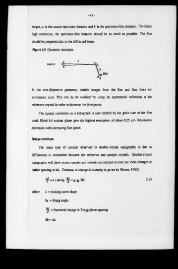
height, a is the source-specimen distance and b is the specimen-film distance. To obtain
high resolution, the specimen-film distance should be as small as possible. The film
[image:43.410.24.383.14.556.2]should be perpendicular to the diffracted beam.
Figure 2.9 Geometric resolution.
In the non-dispersive geometry, double images from the Kai and Kci2 lines are
sometimes seen. This can be be avoided by using an asymmetric reflection at the
reference crystal in order to decrease the divergence.
The spatial resolution on a topograph is also limited by the grain size o f the film
used. Ilford L4 nuclear plates give the highest resolution, o f about 0.25 pm. Resolution
decreases with increasing film speed.
Image contrast.
The main type of contrast observed in double-crystal topography is due to
differences in orientation between the reference and sample crystals. Double-crystal
topographs will show strain contrast and orientation contrast if there are local changes in
lattice spacing or tilt. Contrast, or change in intensity is given by (Bonse, 1962) a
source
2.14
where k = rocking curve slope
0S = Bragg angle
^ f- = fractional change in Bragg plane spacing