Research Paper
Implementation of Dynamic Dual Input Multiple Output Logic Gates via
Enhanced Logical Resonance in Non-Locally Coupled Duffing Oscillators
P R VENKATESH*
PG & Research Department of Physics, Nehru Memorial College (Autonomous), Puthanampatti, Tiruchirapalli 621 007, Tamilnadu, India
(Received on 27 May 2018; Revised on 21 June 2018; Accepted on 22 June 2018)
Employing second sub-harmonic or super-harmonic resonant force, in the presence of weak driven force, to the first site of N non-locally coupled double well Duffing oscillators, can induce the resonance phenomenon in the first site of coupled systems. In this paper, we report that under appropriate coupling strength and coupling radius, the second sub-harmonic or super-harmonic force coherently drives and enhances the amplitude of the weak driven force throughout the remaining
sites of non-locally coupled network which are free from resonant and driven forces and it is termed as ‘Enhanced Resonance’ (ER). Also we illustrate that under this enhanced resonance condition, if any digital signal having amplitude
greater than or equal to the certain threshold value, is given to the first site of the coupled systems, the signal will propagate throughout the entire coupled network without any attenuation. On the other hand, if we give two digital signals with asymmetric amplitudes instead of single digital signal, both the digital signals are logically added and enhanced at the output
of each of the N coupled systems. This phenomenon is termed as ‘Enhanced Logical Resonance’ (ELR) which mimics dual
input multiple output (DIMO) logic gates. Later, we demonstrate that the output of DIMO logic gate is independent of the way of giving the two inputs either simultaneously to any one of the site or separately to any two of the sites of the N coupled systems and thus paved the way to design dynamic dual input multiple output (DDIMO) logic gates such as AND/NAND, OR/NOR gates via enhanced resonance behaviour. It has also been found that the asymmetric amplitude of the two logical inputs decide the various logical behaviours rather than altering the system parameters.
Keywords: Dynamic Computing; Resonance; Coupled Systems; Logic Gates
*Author for Correspondence: E-mail: [email protected]
Proc Indian Natn Sci Acad 85 No. 1 March 2019 pp. 247-255
Printed in India. DOI: 10.16943/ptinsa/2018/49473
Introduction
Now a day, investigation on designing the sequential logic circuit and combinational logic circuit using dynamical systems has become a challenging, interesting and innovative idea in the modern digital technology. Since various dynamical behaviours of the dynamical system can be exploited for implementing fundamental digital elements, especially basic logic gates which will be the fundamental building block of both sequential as well as combinational logic circuits. During the past two decades, different dynamical systems exhibiting different nonlinear phenomena, especially discrete maps exhibiting chaotic behaviour (Sinha and Ditto, 1998; Munakata
et al., 2002; Ditto et al., 2010; Murali et al., 2009a,
2005), coupled chaotic maps or array of chaotic maps
(Sinha et al., 1998, 2002b), continuous nonlinear dynamical systems exhibiting phenomena such as chaos, synchronization, and stochastic resonance (Sinha and Ditto, 1998; Munakata et al., 2002; Ditto and Sinha, 2015; Sinha and Ditto, 1999; Murali et al., 2009c), piece-wise linear systems exhibiting chaos, synchronization, vibrational resonance and strange non-chaotic attractor phenomena (Murali et al., 2003a; Murali and Sinha, 2007; Venkatesh et al., 2016a, 2016b, 2017a) and coupled dynamical systems exhibiting sub-harmonic and super-harmonic resonance behaviours (Venkatesh et al., 2017b) can be employed for this purpose. The exploitation of the various behaviours of the nonlinear dynamical system for dynamic computing starts with the pioneer work of Sinha and Ditto (1998, 1999). Then Munakata et
mechanism for building AND, OR, NOT, XOR &
NAND operations and termed it as ‘Chaogate’.
Further, Sinha et al. (2002a, 2002b) emulated the concept of parallel computing architecture using low dimensional system as well as high dimensional system. Following this, Murali et al. (2003b, 2005) demonstrated an experimental module for logistic map to implement all the logic gate operations. Then, they
further realized this ‘Chaos computing’ using the
cooperative phenomena, namely, chaos synchroni-zation and stochastic resonance (Murali et al., 2007, 2009b, 2009c). Recently, the present author along with Venkatesan and Lakshmanan (2016a) obtained the analytical solutions for chaos synchronization phenomenon in uni-directionally coupled Murali-Lakshmanan-Chua circuit system based on which fundamental logic gates using analytical equations have been demonstrated. To an extent, Ditto et al. (2010) demonstrated that the dynamical evolution of Chaogate could yield half adder/subtractor and full adder/subtractor operations.
Later on, the present author along with Venkatesan (2016b) demonstrated the fundamental logic gates using the analytical solutions of the vibrationally resonanced Murali-Lakshmanan-Chua (MLC) system. Following this, the present author along with Venkatesan and Lakshmanan (2017a) analytically discussed dynamic logic gates and R-S flip-flop circuit using the quasi-periodically driven MLC system. In the mean time, they employed the resonance behaviours, namely, sub-harmonic and super-harmonic resonances in globally coupled Duffing oscillators for implementing dual input multiple
output dynamic logic gates which can meet out ‘fan out limit’ in statically wired hardware(Venkatesh et
al., 2017b). In all the earlier studies of the present
author, the idea of dynamic logic gates has been successfully explained by imposing constraints on the two logical inputs rather than altering system parameters. In an overview, dynamic computing can be realized in systems ranging from physical maps or systems (Sinha and Ditto, 1998, 1999; Munakata et
al., 2002; Venkatesh et al., 2017a) to electronic
circuits (Murali et al., 2003a, 2009a, 2005, 2003b; Ditto et al., 2010), then extended to nano mechanical system (Guerra et al., 2010), chemical system (Sinha
et al., 2009), optical system (Sinha et al., 2002a,
2002b; Singh and Sinha, 2011, Perrone et al., 2012; Chlouverakis and Adams, 2005) and gene network
(Dari et al., 2011a, 2011b, 2011c; Kia et al., 2015; Sharma et al., 2014).
The aim of this paper is to demonstrate how the non-locally coupled double well Duffing oscillators can be effectively utilized in designing dual input multiple output dynamic logic gate (DIMO) via enhanced resonance phenomenon, namely, sub-harmonic and super-harmonic resonances which have been discussed previously by the present author for globally coupled system (Venkatesh et al., 2017b). The purpose of choosing this DIMO dynamic logic gate using resonanced non-locally coupled system is an alternative to DIMO dynamic logic gate by resonanced globally coupled system. Our system has the following advantages, namely, (i) additional control parameter namely, coupling radius r which can also be used to control the logic gate behaviours, (ii) availability of precise digital signal propagation region only for a certain value of coupling radius r, (iii) increasing the chance of getting DIMO logic gate behaviour at lower value of system parameters say resonant force amplitude f2, coupling strength and threshold amplitude of digital signal FT compared to DIMO by globally coupled system and (iv) increasing the chance of getting DIMO logic gate behaviour region for a fixed coupling strength while changing the coupling radius r value. Also it has been demonstrated that the logic behaviour is independent of the way of giving the inputs either simultaneously to any one of the sites or separately to any two of the sites in the N coupled system provided that the input amplitude should be greater than or equal to the greatest threshold value of the N sites.
Non-locally Coupled Double well Duffing Oscillators
We considered a simple N non-locally coupled double well Duffing oscillators represented as,
2 0
i i i
x x x
3
1( 1 sin 1 2 sin 2 )
i
x f t f t
, 2j i P
j i
j i P
x x
P
(1)of the non-linearity of the oscillator, f1 is the strength of the driving force with frequency 1, f2 is the strength of the second external force with high or low frequency2 compared to first driving force, is the coupling strength, and P specifies the number of neighbors in each direction on a ring so that the coupling radius r = P/N. Here xi(t) represents the state vector of the ith oscillator.
1 decides the site to
which the bi-harmonic forces is to be given. Here the bi-harmonic forces are given only to the first site alone and hence1 = 1 for i = 1 and for all other i‡1,1= 0. For numerical discussion, the parameters are fixed as N = 10, = 0.5,02 = -1, = 1, f
1 = 0.05 and1 =
1. The dynamics of the above non-locally coupled systems are seem to be identical to that of the globally coupled network in the absence of coupling strength (i.e., = 0) and external forces (i.e., f1 = f2 = 0) (Venkatesh et al., 2017b). Further, the effect of external forces (f1 and f2) and coupling strength () make the non-locally coupled systems to exhibit a similar enhanced resonance phenomenon as that of the globally coupled systems for certain coupling radius r (Venkatesh et al., 2017b).
Enhanced Resonance in Non-Locally Coupled Double Well Duffing Oscillators
Optimal amplitude of the high/sub-harmonic as well as low/super-harmonic frequency second harmonic driving applied to the first coupled system enhances the response of all the other coupled systems to the first harmonic weak signal. To illustrate the occurrence of resonance phenomenon in the first site and its extension to all the other coupled sites, a second low as well as high frequency harmonic force is included only to the first oscillator.
The response of all the non-locally coupled systems to the high as well as low frequency input driving signal f2Sin2t can be evaluated by calculating the corresponding sine Bi
s and cosine components
Bi
c respectively of the coordinate variations xi(t)
(output signal of ith oscillator). For the ith oscillator,
the sine constituent of the output signal (Venkatesh et
al., 2017b),
1 0
2
( ) sin ,
nT i
s i
B x t tdt
nT
(2)and the cosine constituent of the output signal (Venkatesh et al., 2017b),
1 0
2
( ) cos ,
nT i
c i
B x t tdt
nT
(3)For the frequency 1 = 1.0 with n = 20, the above sine and cosine constituents are evaluated. Then, we finally obtain the dependencies on f2 of both the response amplitude Qi as,
2 2
1
,
i i
s c
i
B B
Q
f
(4)
where T = 2/1 and n is an integer (Venkatesh et
al., 2017b).
Numerical simulation of the system (1) is performed using Runge-Kutta fourth order (RK IV order) algorithm. The response of the entire systems to second periodic driving forces is analyzed by varying the amplitude f2 in steps of 0.1 for the time period of 20T using the Eqs. (2), (3) and (4). It has been observed that for an appropriate low or high frequency second harmonic force applied to the first site of the non-locally coupled systems, one can induce a maximum response to a particular second harmonic force amplitude f2, namely, resonance phenomenon in the first driven site and thus enhance the resonance phenomenon to all the N oscillators for an appropriate coupling strength and coupling radius. This resonance phenomenon can be studied by measuring the response amplitude Qi for all the N sites using the Eqs. (2), (3) and (4). For analysis, the various parameters have been chosen as N = 10, = 0.5,02
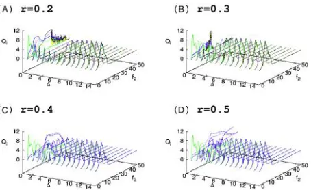
= -1, = 1, f1 = 0.05, 1 = 1,2 = 1/2 for low frequency response, 2 = 21 for high frequency response, r = 0.2, 0.3, 0.4, 0.5 and n=20T.
coupling strength, the entire N coupled sites show a
coherent resonance and it is termed as ‘Enhanced Resonance’. Figs. 1 and 2 show the resulting
response of the non-locally coupled system (1) to the weak periodic signal f1= 0.05, as influenced by the high and low frequency force f2 in the range 0 < f2 < 50 for the coupling strength range 0 << 15 with coupling radius r = 0.2, 0.3, 0.4, 0.5 respectively. Thus occurrence and enhancement of resonance from the first site to the remaining sites shows the propagation of the weak signal throughout the coupled network in biological or network systems. In addition to the enhancement of weak signal f1 under resonance condition, any other digital signal with appropriate amplitude given to any one of the sites of this coupled system should also be enhanced or mimicked at the output of all the sites of the coupled network. This confirms the propagation of single digital signal or logically added two digital signals throughout the enhanced sub/super-harmonic resonanced coupled
system and this phenomenon is termed as ‘Enhanced Logical Resonance’ which mimics dual input multiple
output (DIMO) logic gate.
Implementation of Dynamic Dual Input Multiple Output (DDIMO) Logic Gate via Enhanced Resonance
For some situations, the output of the experimental logic gate can only drive a finite number (called fan-out limit) of inputs to other gates. Also to get different logical operations, the parameter of the system or rewiring the circuit or circuit elements are to be carried out. Taking account of these two limitations, a threshold mechanism to the logical inputs to obtain dynamic DIMO logic cell or gate is proposed (Venkatesh et al., 2017b). Under enhanced resonanced state (i.e., either sub-harmonic or super-harmonic resonance), system (1) can act as a multiple output logic cell and thus performs different logical operations, say, AND/NAND and OR/NOR. Before performing various logical operations, one has to check whether the coupled system (1) can be able to admit/ propagate a square wave or digital signal throughout its sites (i=1 to 10). For that purpose, the system equation (1) is modified as
2 3
0 1
i i i i
x x x x
1 1 2 2 2
(f sin t f sin t) f t( )
, 2j i P
j i
j i P
x x
P
(5)where f(t) is a random square wave or digital signal of amplitude +F to -F and2 decides the site to which the digital signal is given as an input. For example, if
Fig. 1: Response amplitude diagram for ten non-locally coupled Duffing oscillators resonated by high frequency second harmonic force f2 of frequency2 = 2 1 = 2 with different amplitudes for different coupling strengths. (A) Corresponds to r = 0.2 and (B) corresponds to r = 0.3. In (A) and (B), green line (solid line) represents i = 1; blue line (long dash line) represents i = 2, 10; pink line (short dash line) represents i = 3, 9; sky blue line (dotted line) represents i = 4, 8; yellow line (long dash with dotted line) represents i = 5, 7; black line (short dash with dotted line) represents i = 6. (C) Corresponds to r = 0.4 and (D) corresponds to r = 0.5. In (C) and (D), green line (solid line) represents i = 1; blue line (long dash line) represents i = 2, 3, 4, 5, 7, 8, 9, 10; pink line (short dash line) represents i = 6
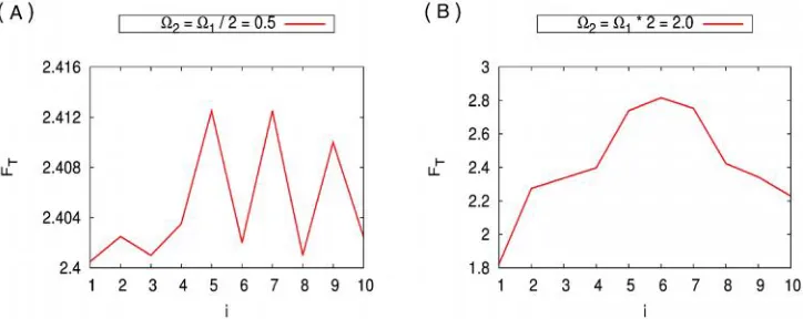
[image:4.612.318.549.81.221.2] [image:4.612.68.295.415.554.2]f(t) is given to the first site (i=1), then 2 = 1 and for all other i‡1, 2 will be 0. In general,2 = 1 when f(t) is given to the nth site (i.e., i = n) and for all other i ‡ n, 2 will be 0. For un-damped propagation, one must operate the above non-locally coupled oscillators in the resonance region by fixing f1 = 0.05, f2 = 7.4,2 =1/2 and = 15 to get coherent behaviour for a low frequency second harmonic force. It has been numerically found that for propagating a random digital signal throughout the N oscillators, the amplitude of the signal given to the first site must meet certain necessary condition. In other words, only the random digital signal given to the first site i = 1 having an amplitude greater than or equal to the threshold value FT = 2.4005 (see Fig. 3A) alone shows significant propagation. For digital signal amplitude F < -FT, all the N oscillators will show output xi < 0 which will be treated as logic 0 and for the amplitude F > FT, the output will be xi > 0, treated as logic 1. This shows that to change the attractor from negative potential well to positive well, a threshold value of F > FT is to be needed and for the reverse case, a threshold value of F < -FT is to be employed. Thus, by giving the digital signal to the various other sites i = 2 to 10 individually, the corresponding threshold value/ amplitude of FT is numerically evaluated and plotted as shown in Fig. 3A. Similarly for the high frequency second harmonic signal, the threshold value of the digital signal that has been given as an input to various sites (i = 1 to 10) separately, is numerically evaluated and plotted as shown in Fig. 3B.
From the Figs. 3A and 3B, it has been found that for propagating the digital signal throughout all
the N sites by giving the digital input to any one of the sites irrespectively, the threshold amplitude FT of the input signal should be greater than or equal to the maximum of the ten sites. In other words, for better digital signal propagation irrespective of the input given to any one of the sites, the amplitude of the input digital signal should be greater than or equal to the greatest peak value of the curve i.e., FT > 2.4125 (see Fig. 3A) for low frequency second harmonic force and FT> 2.816 (see Fig. 3B) for high frequency second harmonic force.
According to this scheme of threshold mechanism (Venkatesh et al., 2017b), to construct dynamic DIMO logic gate, the non-locally coupled N oscillators exhibiting coherent resonance mimics the logic gate or cell with N more or less coherent outputs is considered here. For any logical operations, two input signals are needed. Thus, here two random square waves are used as two input signals instead of f(t) in Eq. (5). With these input signals, the four possible input combinations (0 or -F, 0 or -F), (0 or -F, 1 or +F), (1 or +F, 0 or -F), (1 or +F, 1 or +F) merge into three different input combinations (0,0), (0,1)/(1,0) and (1,1). The low input is taken as1for logical 0 and the high input as2 for logical 1. From the earlier discussion in this section, for AND or OR operation, the two inputs are logically added and the resultant digital signal should be such that for the logical 0 state the amplitude must be less than or equal to -FT and for the logical 1 state the amplitude must be greater than or equal to FT. In addition to that, this logically added signal should propagate throughout the N oscillators without damping in its amplitude. This is
[image:5.612.128.490.548.692.2]possible only if all the non-locally coupled oscillators are set in either sub-harmonic or super-harmonic resonance state. Thus the logical low 0 output of the entire N coupled sites are considered as xi < 0 and the logical high 1 outputs are taken as xi > 0 with i = 1, 2...10. For NAND/NOR operations, the logical low 0 output is taken as xi > 0 and the logical high 1 output is taken as xi < 0 with i = 1,2...10. The three possible input combinations with the corresponding outputs for AND and OR gates are represented (Venkatesh et
al., 2017b) as
AND Gate:
1 1 FT,
(6a)
1 2 FT,
(6b)
2 2 FT.
(6c)
From Eq. (6c),2> FT/2. On substituting in Eq. (6b),1< -3FT/2 and also satisfies Eq .(6a). Thus, logic 0 and logic 1 value of the inputs for AND gate should be
1
3 , 2
T
F
2 .
2
T
F
(7)
OR Gate:
1 1 FT,
(8a)
1 2 FT,
(8b)
2 2 FT.
(8c)
With Eq. (8a),1> -FT/2. On substituting in Eq. (8b),2< 3FT/2 and also satisfies Eq. (8c). Thus for OR gate, the logic 0 and logic 1 of the inputs should be
1 ,
2
T
F
2
3 . 2
T
F
(9)
For numerical simulations, the value of FT is chosen to be greater than or equal to 1.8225 (see Fig. 3B and choose FT = 3.0 here) corresponding to the system parameters f1 = 0.05, f2 = 9.8,2 = 21 = 2 and = 13 with the two logical inputs given simultaneously to the first site (i = 1) of the ten non-locally coupled Duffing oscillators. For AND operation, the logic 0 and logic 1 of the inputs are evaluated from the above Eq. (7) and are found to be
1= –4.5 and2= 1.5. The AND response of all the ten oscillators for the various random combinations of the two digital inputs are shown in Fig. 4. Similarly, one can get an identical AND response for low frequency second harmonic force f2 of frequency2 =1/2 = 0.5 with system parameters f1 = 0.05, f2 = 7.4, = 15 and FT> 2.4005 (say here FT = 3.0).
Figure 5 illustrates the logical OR operation for two random input signals with logic 0 as1= –1.5
and logic 1 as2= 4.5 (using Eq. (9)) corresponds to FT = 3.0 (FT> 1.8225 for high frequency force f2 and FT> 2.4005 for low frequency force f2) for the ten non-locally coupled system (5). From Figs. 3A and 3B, the threshold value of the digital signal that has been given as input to various sites of the ten non-locally coupled Duffing oscillators is not same. In order
[image:6.612.311.545.468.644.2]to give the two inputs in a dynamic way such that the inputs are given either simultaneously or separately to any of the sites irrespective of their order/number (i), the value of the FT should be greater than or equal to the maximum of the all the ten sites (For high frequency resonant system FT> 2.816 (see Fig. 3B) and for low frequency resonant system FT> 2.4125 (see Fig. 3A) respectively, here FT = 3.0 for both low as well as high frequency resonant system). Thus for AND operation, the logic 0 and logic 1 of the input signal becomes1= –4.5 and2= 1.5 respectively. Fig. 6 demonstrates the dynamic dual input multiple (say ten outputs) output AND logic gate corresponds to high frequency resonant system (5) for the system parameters f1 = 0.05, f2 = 9.8,2 = 21 = 2 and = 13. Here, the logic 0 and logic 1 states of the input signals shown in Fig. 6A are obtained based on the random number function which generates a random number between 0 and 1 with uniform distribution and having the mean converges to 0.5. At any instant of time, if the random number is less than or equal to 0.5 (mean value), then the input is taken as logic 0 (I1 = I2 = –4.5), otherwise the input is taken as logic 1 (I1
= I2 = 1.5). Then the overall statistical analysis of switching behaviours especially, probability of
occurrence of ‘1’ state (I1 = I2= 1.5) and ‘0’ state (I1
= I2= –4.5) corresponding to the inputs in Fig. 6A are
to be analysed to check whether the switching is
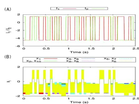
Fig. 5: Logical OR operation for two random inputs and its persistence throughout ten non-locally coupled Duffing oscillators resonated by a low frequency second harmonic force f2 of frequency 2 =1/2= 0.5. (A) Two random input signals (Green and Red) given to the first site (i.e., i = 1) of the coupled systems and (B) 2-D plot between Time in seconds and output states xiof N = 10 oscillators
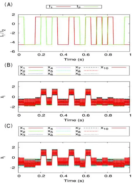
Fig. 6: Logical AND operation for two random inputs and its persistence throughout ten non-locally coupled Duffing oscillators resonated by a high frequency second harmonic force f2 of frequency 2= 21 = 2. (A) Two random input signals (Green and Red), (B) 2-D plot between Time in seconds and output states xi of the entire (ten) oscillators for the two inputs in figure (A) given separately to two different oscillators such that I1 to i=1 and I2 to i=2 respectively, and (C) same 2-D plot for the same two inputs in figure (A) given to two different oscillators separately such that I1 to i=5 and I2 to i=10 respectively
uniform or not. In order to analyse this switching
behaviour, the total number of events (including ‘0’ state and ‘1’ state of the input signal) occurred during
the time period 0 to 1 sec is to be evaluated. Here, it is found to be 201000. Then the probability of
occurrence of ‘0’ state is calculated as P(0 or –4.5) = 0.602 and that of ‘1’ state is P(1 or 1.5) = 0.398 for
the first input signal (I1) (red solid line in Fig. 6A). Similarly, for the second input signal (I2) (green dotted
line in Fig. 6A) the probability P(0 or –4.5) and P(1 or
[image:7.612.320.546.81.394.2] [image:7.612.68.300.81.254.2]increases.
Similar response can be obtained for low frequency resonant system with the system parameters f1 = 0.05, f2 = 7.4 and = 15 respectively. Similarly, one can also get the DDIMO OR behaviour with the low as well as high frequency resonant system for the various combinations of the logical inputs1=
–1.5 (logic 0) and2= 4.5 (logic 1) respectively.
Conclusions
In a brief overview, we have shown the occurrence and coherent enhancement of sub/super harmonic resonance in ten non-locally coupled oscillator which depends on the coupling strength and coupling radius. Also, we have numerically illustrated the digital response of all the sites of the ten non-locally coupled networks for the random digital signal that too given as an input to any one of the ten sites. Further, it has been found that for the better response of the digital input or in other words mimicking the digital input at
the output of N sites, the amplitude of the digital input should always be equal or greater than the threshold value FT. To an extent, we have also enumerated the idea of implementation of DDIMO logic gate structures which is one of the significance of sub/ super harmonic resonance. In particular, we have shown the direct and flexible implementation of the basic DDIMO logic gates AND/NAND and OR/ NOR using the non-locally coupled oscillator system under resonanced condition by simply altering the high or positive and low or negative amplitude of the input signals without altering the system parameters. Such a scheme of implementation of basic DDIMO logic gates for parallel processing digital circuits may serve as ingredients of a general purpose device and are more flexible than statically wired hardware.
Acknowledgments
I give thanks to Prof. K Murali, Dr. A Venkatesan and Prof. M Lakshmanan for useful discussion.
References
Chlouverakis K E and Adams M J (2005) Optoelectronic realisation of NOR logic gate using chaotic two-section lasers Electron Lett 41 359
Dari A, Kia B, Wang X, Bulsara A R and Ditto W L (2011a) Noise-aided computation within a synthetic gene network through morphable and robust logic gates Phys Rev E 83 041909
Dari A, Kia B, Bulsara A R and Ditto W L (2011b) Logical stochastic resonance with correlated internal and external noises in a synthetic biological logic block Chaos 21 047521
Dari A, Kia B, Bulsara A R and Ditto W L (2011c), Creating morphable logic gates using logical stochastic resonance in an engineered gene network Europhysics Letters 93 18001
Ditto W L, Miliotis A, Murali K, Sinha S and Spano M L (2010) Chaogates: Morphing logic gates that exploit dynamical patterns Chaos 20 037107
Ditto W L and Sinha S (2015) Exploiting chaos for applications Chaos 25 097615
Guerra D N, Bulsara A R, Ditto W L, Sinha S, Murali K and Mohanty P (2010) A noise-assisted reprogrammable nanomechanical logic gate Nano Lett 10 1168
Kia B, Lindner J F and Ditto W L (2015) Nonlinear dynamics based digital logic and circuits, Frontiers in Computational
Neuro Science 9 PMC4432664
Munakata T, Sinha S and Ditto W L (2002) Chaos computing: Implementation of fundamental logical gates by chaotic elements, IEEE Trans Circuit & Systems I:Fundamental Theory and Applications 49 1629
Murali K, Sinha S and Ditto W L (2003a) Implementation of
NOR gate by a chaotic Chua’s circuitInt J Bif Chaos 13 2669
Murali K, Sinha S and Ditto W L (2003b) Realization of the fundamental NOR gate using a chaotic circuit Phys Rev E
68 016205
Murali K, Sinha S and Ditto W L (2005) Construction of a reconfigurable dynamic logic cell Pramana 64 433
Murali K and Sinha S (2007) Using synchronization to obtain dynamic logic gates Phys Rev E 75 025201(R)
Murali K, Miliotis A, Ditto W L and Sinha S (2009a) Logic from nonlinear dynamical evolution Phys Lett A 373 1346
Murali K, Rajamohamed I, Sinha S, Ditto W L and Bulsara A R (2009b) Realization of reliable and flexible logic gates using noisy nonlinear circuits Appl Phys Lett 95 194102
Murali K, Sinha S, Ditto W L and Bulsara A R (2009c) Reliable logic circuit elements that exploit nonlinearity in the presence of a noise floor Phys Rev Lett 102 104101
that exploits noise and polarization bistability in an optically injected VCSEL Opt Express 20 22692
Sharma A, Kohar V, Shrimali M D and Sinha S (2014) Realizing logic gates with time-delayed synthetic genetic networks Nonlinear Dynamics 76 431
Singh K P and Sinha S (2011), Enhancement of logical responses by noise in a bistable optical system Phys Rev E 83 046219
Sinha S and Ditto W L (1998) Dynamics based computation Phys Rev Lett 81 2156
Sinha S and Ditto W L (1999) Computing with distributed chaos Phys Rev E 60 363
Sinha S, Munakata T and Ditto W L (2002a) Flexible parallel implementation of logic gates using chaotic elements Phys Rev E 65 036216
Sinha S, Munakata T and Ditto W L (2002b) Parallel computing with extended dynamical systems Phys Rev E 65 036214
Sinha S, Cruz J M, Buhse T and Parmananda P (2009) Exploiting the effect of noise on a chemical system to obtain logic
gates Europhysics Letters 86 60003
Venkatesh P R, Venkatesan A and Lakshmanan M (2016a) Analytical treatment for synchronizing chaos through unidirectional coupling and implementation of logic gates Pramana 86 1195
Venkatesh P R and Venkatesan A (2016b) Vibrational resonance and implementation of dynamic logic gate in a piecewise-linear Murali-Lakshmanan-Chua circuit Communications in Nonlinear Science and Numerical Simulation 39 271
Venkatesh P R, Venkatesan A and Lakshmanan M (2017a) Design and implementation of dynamic logic gates and R-S flip-flop using quasiperiodically driven Murali-Lakshmanan-Chua circuit Chaos 27 033105