Low Power High Speed for
LCD
Flat Panel Display
Application
Rajeev Thakur
Associate professor NIIST Bhopal
Piyush Soni
M.Tech Scholar NIIST Bhopal
ABSTRACT
A low power buffer amplifier for LCD panel driving system is presented. The proposed architecture has self-biased RAIL TO RAIL complementary differential pair for full input output swing, and class B push-pull output driving stage which is suitable for large and small size liquid crystal display, compensation capacitor and resistance are used to improve the settling time and slew rate of the buffer amplifier by stabilizing phase margin, an experimental prototype is simulated using cadence specter in .35 µm CMOS technology which draws only 8 µm static current and provide a settling time of 2.8 µs and rising and 3 µs during four the act area for the design of the buffer is 49*60 µm With power supply of 3.3 it with stand with 1000 pF load capacitance the power consumption of the amplifier under static condition is 66µW.
Keywords
Rail Operational Amplifier
1.
INTRODUCTION
With increasing demand of high speed low power liquid crystal display in recent years, we have to match with these requirements to consummate the market demand. LCD driver generally contains shift registers, input register's, data latch, level shifter , digital to analog converter, Pre-Emphasis, and analog buffers the output buffer amplifier is vigorously affects the speed, resolution, voltage swing and power dissipation [12],[4],[8],[9]. For each pixel we a buffer amplifier is required so as the number of pixel increases the number of buffers on the panel to drive increases, nowadays battery operated portable devices are acclimated to increase the performance and to elongate the battery life we require low-power high-speed buffer amplifier LCD output buffer amplifier are realized by operational amplifier in unity gain configuration generally RAIL TO RAIL operational amplifiers are acclimated to get plenary output swing RAIL TO RAIL operation amplifiers are consist of complimentary differential amplifiers at first stage and a summing current source at second is stage with generally kenned as folded cascaded architecture then the output is stage which are this work in class B and class AB push pull stage.
2.
PROPOSED BUFFER DRIVING
SCHEME
Generally introducing zero in transfer function of buffer amplifier using phase compensation register & output load Capacitance it makes the buffer stable but the slew rate is limited as due to small slew rate the settling time for large
A typical two stage operational amplifier requires compensation for the stability some buffer amplifier's takes the output node as the dominant to achieve the stability without Miller capacitance[3,6] however charge conservation technique is commonly used in some LCD driver to reduce the dynamic power dissipation[1,2]
3.
ZERO COMPENSATION
TECHNIQUE
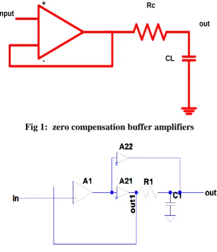
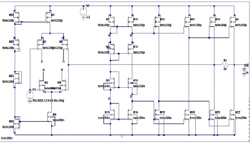
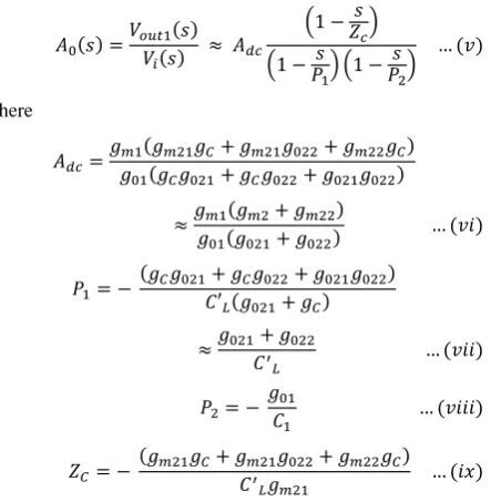
Zero compensation technique is generally used to get the dominant pole in buffer amplifier figure 1 shows a buffer amplifier with zero compensation. And fig 2 shows the configuration of proposed buffer amplifier using zero compensation technique. Fig 4 shows the schematic of proposed buffer amplifier
input
Rc
CL
out +
-Fig 1: zero compensation buffer amplifiers
[image:1.595.321.534.429.676.2]Before compensation
After compensation P1
P2
Zc
Frequency
G
a
in
(d
b
[image:2.595.125.488.74.234.2])
Fig 3: Frequency response of buffer amplifier
Fig 4: Schematic of proposed buffer amplifier
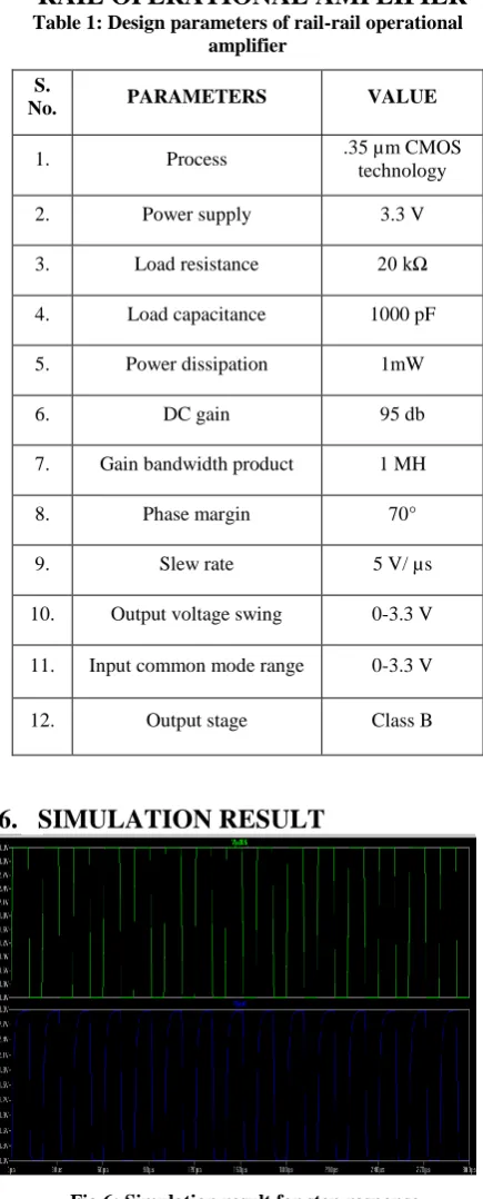
In figure 3 solid line shows frequency characteristic before compensation and dotted line after compensation, As dominant pole P1 shifted towards origin as with increasing load capacitance means gain bandwidth will decrease it also makes system unstable and degrade phase margin, for proper operation of buffer for high speed phase margin should be in between 70° to 45° generally they prefer 60° phase margin for high speed low-power buffer amplifier design here using " " introduces required phase margin, it introduce a zero in transfer function.
This is called as zero compensation technique for large phase margin, it is generally used when we does not use them Miller capacitor in between differential amplifier and output is stage of differentiated amplifier. The value of zero located to left the most of unity gain bandwidth to the college RGB
For 70° phase and margin ζ and amplifier is stable, for ζ
the phase margin is approximately given as I moved to women in
PM and settling time =
[image:2.595.58.552.258.542.2]4.
SMALL SIGNAL ANALYSIS OF
PROPOSED
gm1Vi Vi
g01
c1 gm21 V1
go21
C21 Vout1
gc
Vout
gm22 V1 g022
[image:3.595.55.287.72.201.2]CL’ =[CL+C22
Fig 5: Small signal model of proposed buffer.
[image:3.595.61.283.292.519.2]The small signal of the proposed driving scheme is shown in figure 5 when we does not count the the transconductance of complimentary differential pair is gm1, and gm21,gm22 are the transconductance of two competitors, and g01,g021 and g022 are the output conductance, and are the paracetic capacitance.
The open loop transfer function of the buffer ,
where
The above Equivalent circuit contains three poles and zero the third pole is far away from other poles and zero, so it is neglected, g01,g021 and g022 conductance are much smaller than gc, the parasitic capacitance is also much smaller than load capacitance these aproximations are taken for the analysis.
The closed loop transfer functiom of buffer,
the relation between Vout1 and Vout2 from the figure 5 is expressed as:
the closed loop transfer function of overall block as shown in figure 4:
The zero from the data transfer function is neglected as it is far away from the dominant pole.
and it is equivalent to second o order transfer function so,
5.
DESIGN PARAMETERS OF
RAIL-RAIL OPERATIONAL AMPLIFIER
Table 1: Design parameters of rail-rail operational amplifier
S.
No. PARAMETERS VALUE
1. Process .35 µm CMOS
technology
2. Power supply 3.3 V
3. Load resistance 20 kΩ
4. Load capacitance 1000 pF
5. Power dissipation 1mW
6. DC gain 95 db
7. Gain bandwidth product 1 MH
8. Phase margin 70°
9. Slew rate 5 V/ µs
10. Output voltage swing 0-3.3 V
11. Input common mode range 0-3.3 V
12. Output stage Class B
[image:4.595.55.273.95.635.2]6.
SIMULATION RESULT
Fig 6: Simulation result for step response.
[image:4.595.318.532.263.447.2]Fig 7: Simulation result for triangular response.
Fig 8: Current at trail end of PMOS & NMOS differential pair.
[image:4.595.53.272.378.615.2] [image:4.595.315.532.479.651.2]Fig 9: Power consumption differential pair during static condition.
[image:5.595.315.532.73.263.2]Fig 11: simulation result of common mode rejection ratio.
[image:5.595.315.534.274.668.2]Fig 11: Frequency response of proposed buffer amplifier.
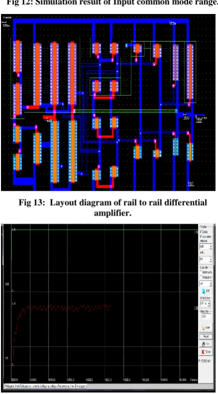
[image:5.595.53.271.284.453.2]Fig 12: Simulation result of Input common mode range.
Fig 13: Layout diagram of rail to rail differential amplifier.
[image:5.595.55.270.480.647.2]7.
COMPARISON TABLE
Table 2
:
Comparison TableRef [20] Ref [3] Ref.[ 4] Ref.[1 ] This work is CMOS technology (µm)
.6 .6 .6 .5 .35
Supply
voltage 5V 5 V 5 V 5 V .33 V
Max load capacitor 680 pF 170 pF 30 pF 1000 pF 1000 pF Quiescent current 30
µA 5 µA 8.2
µA 32 µA 8 µA
Power 150 µW 75 µW 150 µW 160
µW 66 µW
Settling time 1.2 µs 9.6 µs 8.2
µs .7 µs 3.2 µs
Input-output range [V] .15/4 V .15/4. 8V .5/4.5
V 0/5 V
0/3.2 V Input-output range [VDD%]
77% 93% 80% 100 % 97 %
Slew rate _ _ _ _ 7 V /
µs
Active area
[µm²] N/A N/A N/A 73 × 91 50 ×60
8.
CONCLUSION
Self-biased high-speed low-power rail to rail buffer amplifier for LCD is proposed work under class B operation which is suitable for small and large size LCD panel, the Zero compensation is used to enhance the slew rate and settling time the compensation resistor value should be optimized to get the optimal value of slew rate and phase margin, as with large value of compensation resistor we get adequate phase margin but it will increase settling time and vice versa. A prototype of this buffer is implemented on .35 µm CMOS technology it draws only is 8 µA static current. The buffer draws little static current but has a large driving capability during transition phase , full swing is obtained by RAIL TO RAIL operational amplifier and enlarge driving capability is obtained by the use of two comparators. The buffer is 3 µs of rising settling time and 3.2 µs of falling settling time, the active area occupied by the buffer is approximately 3600 µm². The performance of the proposed buffer is compared with previous buffer it is superior in power consumption, low static current and small settling time.
9.
REFERENCES
[1] Alfio Dario Grasso, Member, IEEE, Davide Marano, Fermin Esparza-Alfaro, Antonio J. Lopez-Martin, Senior Member, IEEE, Gaetano Palumbo, Fellow, IEEE, "Self-Biased Dual-Path Push-Pull Output Buffer Amplifier for LCD Column Drivers" IEEE transactions on circuits and systems—i: regular papers, vol. 61, no. 3, march 2014
[2] D. J. R. Cristaldi, S. Pennisi, and F. Pulvirenti, Liquid Crystal Display Drivers: Techniques and Circuits. New York: Springer, 2009.
[3] M.-C. Weng and J.-C. Wu, “A compact low-power Rail-to-Rail class-B buffer for LCD column driver,” IEICE Trans. Electron., vol. E85-C, no. 8, pp. 1659–1663, Aug. 2002.
[4] T. Itakura and H. Minamizaki, “A two-gain-stage amplifier without an on-chip Miller capacitor in an LCD driver IC,” IEICE Trans. Fundam., vol. E85-A, no. 8, pp. 1913–1920, Aug. 2002.
[5] C.-W. Lu, “High-speed driving scheme and compact high-speed low-power Rail-to-Rail class-B buffer amplifier for LCD applications,” IEEE J. Solid-State Circuits, vol. 39, pp. 1938–1947, Nov.2004.
[6] C.-W. Lu, C.-M. Hsiao, and P.-Y. Yin, “Voltage selector ad a linearityenhanced DAC-embedded op-amp for LCD column driver ICs,” IEEE J. Solid-State Circuits, vol. 48, pp. 1475–1486, Jun. 2013.
[7] J. Ramirez-Angulo, A. Torralba, R. G. Carvajal, and J. Tombs, “Low-voltage CMOS operational amplifiers with wide input-output swing based on a novel scheme,” IEEE Trans. Circuits Syst. I, Fundam. Theory Appl., vol. 47, no. 5, pp. 772–774, May 2000.
[8] S. Karthikeyan, S. Mortezapour, A. Tammineedi, and E. K. F. Lee, “Low-voltage analog circuit design based on biased inverting opamp configuration,” IEEE Trans. Circuits Syst. II, Analog Digit. SignalProcess., vol. 47, no. 3, pp. 176–184, Mar. 2000.
[9] G. A. Rincon-Mora and R. Stair, “A low-voltage, rail-to-rail, class-AB CMOS amplifier with high drive and low output impedance characteristics,”IEEE Trans. Circuits Syst. II, Analog Digit. Signal Process., vol. 48, no. 8, pp. 753–761, Aug. 2001.
[10] K. J. de Langen and J. H. Huijsing, “Compact low-voltage power-efficient operational amplifier cells for VLSI,” IEEE J. Solid-State Circuits, vol. 33, no. 10, pp. 1482–1496, Oct. 1998.
[11] A. Torralba, R. G. Carvajal, J. Ramirez-Angulo, J. Tombs, and J. Galan, “Class AB output stages for low voltage CMOS opamps with accurate quiescent current control by means of dynamic biasing,” in Proc. IEEE ICECS’01, Sep. 2001, vol. 2, pp. 967–970.
[12] F. You, S. H. K. Embabi, and E. Sánchez-Sinencio, “Low-voltage class AB buffers with quiescent current control,” IEEE J. Solid-State Circuits, vol. 33, no. 6, pp. 915–920, Jun. 1998.
[14]T. Stockstad and H. Yoshizawa, “A 0.9-V 0.5-A rail-to-rail CMOS operational amplifier,” IEEE J. Solid-State Circuits, vol. 37, no. 3, pp. 286–292, Mar. 2002. [15]W. Aloisi, G. Giustolisi, and G. Palumbo, “A 1-V CMOS
output stage with excellent linearity,” Electron. Lett., vol. 38, no. 22, pp. 1299–1300, Oct. 2002.
[16]R. van Dongen and V. Rikkink, “A 1.5 V class AB CMOS buffer amplifier for driving low-resistance loads,” IEEE J. Solid-State Circuits, vol. 30, no. 12, pp. 1333–1338, Dec. 1995.
[17]G. Palumbo, “1.2V CMOS output stage with improved drive capability,” Electron. Lett., vol. 35, no. 5, pp. 358– 359, Mar. 1999.
[18]G. Palmisano, G. Palumbo, and R. Salerno, “A 1.5-V high drive capability CMOS Op-Amp,” IEEE J. Solid-State Circuits, vol. 34, no. 2, pp. 248–252, Feb. 1999. [19]P.-C. Yu and J.-C. Wu, “A class-B output buffer for
flat-panel-display column driver,” IEEE J. Solid-State Circuits, vol. 34, pp. 116–119, Jan. 1999.
[20]C.-W. Lu and C. L. Lee, “A low-power high-speed class-AB buffer amplifier for flat-panel-display application,” IEEE Trans. Very Large Scale Integr. (VLSI) Syst., vol. 10, pp. 163–168, Apr. 2002.
[21] C.-W. Lu and P. H. Xiao, “A high-speed low-power Rail-to-Rail buffer amplifier for LCD application,” in Proc. CCECE, Dec. 2006, pp. 709–712.
[22] J.-H.Wang, J.-C.Qiu,H.-Y. Zheng, H.Tsai, C.-Y.Wang, C.-C.Lee, and C.-T. Chang, “A compact low-power high slew-rate Rail-to-Rail class-AB buffer amplifier for LCD driver ICs,” in Proc. EDSSC, Dec. 2007, pp. 397–400.
[23] W.-J. Huang, S. Nagayasu, and S.-I. Liu, “A Rail-to-Rail class-B buffer with DC level-shifting current mirror and distributed Miller compensationfor LCD column drivers,” IEEE Trans. Circuits Syst. I, Reg. Papers,vol. 58, no. 8, pp. 1761–1772, Aug. 2011.
[24] D. Marano, G. Palumbo, and S. Pennisi, “Low-power high-speed Rail-to-Rail LCD output buffer with dual-path push-pull operation and quiescent current control,” Analog Integr. Circuits Signal Process., vol. 65, no. 2, pp. 289–298, Sep. 2010.