Patterning Technology of Ferrite and Insulating Material
in a Single Layer of the Multilayer Ceramic Device
Minami Takato*, Aki Kenmochi, Toshiki Fujino, Ken Saito, Fumio Uchikoba College of Science and Technology, Nihon University, Chiba, Japan.
Email: *[email protected]
Received March 21st, 2012; revised May 27th, 2012; accepted June 10th, 2012
ABSTRACT
Patterning technology of ferrite and insulating material in multilayer ceramic devices is proposed. In the conventional technology, the different ceramic materials such as the ferrite and the insulating material have been prepared in the form of the each different green sheet, and then they have been stacked each other. Otherwise the different material has filled cavities that were formed by a mechanical punching in advanced. In our proposing technology, arbitrary patterning of the different ceramic material inside the same green sheet is possible. In this process, the arbitrary shape of the through pattern is formed in the green sheet of the base material by making use of photo resist films as sacrifice patterns, and then the base material is masked by the patterned photo resist film. After filling the slurry of the different material into the through pattern of the base material passing the resist mask, the pattern of the different ceramic material in the green sheet is achieved. In the present paper, the ferrite magnetic material and the alumina-glass composite material are used. The patterned structure inside the green sheet is obtained. The slurry preparation, the thickness of the mask resist film, and the obtained structure of the green sheet are discussed.
Keywords: LTCC; Ferrite; Patterning; Green Sheet; Photo Resist Film
1. Introduction
In order to satisfy the strong demand of the miniaturiza-tion and high performance of communicaminiaturiza-tion equip- ments, miniaturization and integration of ceramic de- vices have also improved. It is quite advantageous for further miniaturization to introduce different ceramic materials and realize complex three dimensional struc- tures inside the multilayer ceramic component.
However, the utilization of different ceramic materi-als and complex three dimensional structures has been limited. The reason is attributed to the conventional fabrication process. The fabrication process of the mul-tilayer ceramic device is called green sheet process [1], and in the process, mixture of the ceramic powder and organic material is formed into the sheet structure. The conductor is printed and then the multiple sheets are stacked.
For example, Ni-Cu-Zn ferrite is used as the mag-netic material. Then the multilayer ceramic inductor has been developed [2]. Also glass alumina composite is used as insulation material and LTCC (Low Temperature Cofired Ceramic) substrate has been developed [3-7].
Although a number of studies were reported on the cofiring technology of the magnetic material and the insulation material in order to form magnetic circuit and insulating part, the magnetic sheet and the insulation sheet were formed separately and then they were stacked [8]. Otherwise, the different material was filled into the cavity which had been formed by a mechanical punch beforehand [9]. Therefore, the patterning of the different material in the same level of the green sheet in the multilayer ceramic devise has not been achieved.
In conventional multilayer ferrite inductors, the mi-nor magnetic loop causes the degradation of the induc- tance and the Q factor because the internal conductor is filled with the ferrite magnetic material. If nonmagnetic material is patterned and inserted between the conduc-tors of each layer, it is possible to suppress the minor magnetic loop. The mechanism of the minor magnetic loop and the suppression is shown in Figure 1. In the
LTCC substrate, the embedded inductance device and shield and suppressing of the noise can be achieved by making use of the patterning of the magnetic material in the insulating material.
This paper proposed the patterning technology of the different material in a single piece of the green sheet utilizing a photo resist film.
coil pattern
flux loss
magnetic material
non magnetic material pattern
magnetic flux
[image:2.595.94.243.85.339.2]non magnetic material
Figure 1. Suppression mechanism of the minor magnetic loop and introducing the non magnetic material.
2. Patterning Method in a Single Green
Sheet
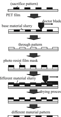
Arbitrary shapes of sacrifice patterns are formed on a carrier film by photo lithographic exposure and devel-opment of the photo resist film in the first step. The rea-son for using the film resist was that the uniform thick-ness was obtained, and the thickthick-ness of the resist film was thicker than that of the liquid resist. Then the slurry mixture of the ceramic powder and the organic material is filled around the sacrifice pattern with the doctor blade method. After drying the obtained sheet, the resist pattern is plasticized by dissolving agent and removed, and then the designed through pattern is formed and the ceramic pattern remains.
Another photo resist film is prepared for covering the patterned ceramic. The reversal pattern is exposed on the resist film and developed. The formed resist film is bond- ed on the ceramic pattern with an alignment equipment of a X-Y-θ stage. The other slurry of the different ce-ramic material is filled around the cece-ramic pattern that is covered with the resist film by the doctor blade method. After drying the sheet and removing the resist, the green sheet with the patterned different ceramic material is achieved. The schematic illustration of the procedure for forming the patterned different ceramic material in the base material is shown in Figure 2.
Different from the conventional process, this technol-ogy is based on the photo lithographic process. Therefore, the miniaturization and flexible pattern designing is
pos-sible. Also, this technology realizes the through structure of the different material inside the same sheet of the base material. Although the conventional patterning techno- logy of electrode material such as screen printing forms bump structure on the sheet, this technology forms the flat surface. The flat surface makes the large number of stacking of the green sheet easier.
3. Experimental Procedure
3.1. Sample Pattern
Two materials of alumina glass composite and ferrite were used in this study. The experimental pattern and the stacked structure are shown in Figures 3 and 4,
respec-tively. 5 pieces of the different material patterns were arranged as is shown in Figure 3. The dimensions of the
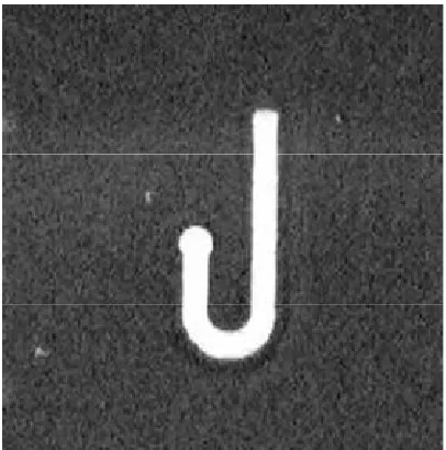
center square were 1.4 mm × 1.4 mm and the dimensions of the peripheral squares were 1.4 mm × 1.1 mm. Also, the pattern of “J” figure was used for the sample pattern
different material pattern drying process different material slurry
photo resist film mask through pattern base material slurry
doctor blade photo resist film
(sacrifice pattern)
PET film
Figure 2. Process for forming the patterned different ce-ramic material in the single layer.
1.4mm 1.1mm
1.4mm
[image:2.595.358.487.333.581.2] [image:2.595.367.481.630.719.2]stacked
2 blank layers
layer of different material pattern
[image:3.595.58.289.86.180.2]3 blank layers
Figure 4. Stacked structure of the patterned different mate-rial inside the base matemate-rial green sheet.
as is shown in Figure 5. This sample was supposed for
the single layer of the multilayer inductor. The base ma-terial was designed for the ferrite magnetic mama-terial and the patterned material was nonmagnetic material. The internal conductor was supposed to be screen printed on the nonmagnetic layer and then the minor magnetic loop between the internal conductors was expected to be sup-pressed.
3.2. Preparation of Powders and Slurries
The weight ratio of the glass powder and the alumina powder in the glass alumina composite material was 63 and 37. The glass powder was composed of SrO-B2O3
-Al2O3-SiO2 and the particle size was about 1 μm. The
particle size of the alumina powder was 0.2 μm. The fer-rite powder was synthesized by calcination process. The start materials were NiO, ZnO, CuO and Fe2O3 and the
molecular ratio was 8.8-32-10-49.2. The ferrite powder was crashed to 0.3 μm by ball mill method.
Mixing the glass powder, the alumina powder, organic solvents and some additives by the ball mill method for 3 hours, poly vinyl butyral (PVB) was added. The ferrite powder was mixed with organic solvents and some addi-tives for 24 hours. After adding PVB binder, the mixing time was 24 hours.
It is often that the glass alumina composite slurry con-tains phosphoric ester as a dispersant agent. However, the phosphoric ester is known as a sintering inhibitor of the ferrite. Therefore, the slurry contained the non phos-phoric ester dispersant.
Different from usual ceramic slurry, filling and pat-terning capability is required in this method. In order to satisfying these requirements, the rheologic properties of both low viscosity and high thixotropy were required. For this reason, the slurry was adjusted to the appropriate property, varying the content of the binder and organic solvent. Moreover, the density of the ferrite is higher than that of the glass alumina composite. Therefore, the weight ratio of the ferrite powder contents was made larger than that of the glass alumina powder in order to adjust similar volume contents. The adjusted slurry com- position is shown in Table 1. The organic solvent was
mixture of toluene, xylene and isopropyl alcohol. Also
additives such as dispersant and plasticizer were used. In the case of the ferrite, two kinds of specified slurry were arranged for each the patterning and the blank layer.
3.3. Patterning Procedure
First step, the photo resist film was exposed and deve- loped for forming the sacrifice pattern that was corres- ponding to the through pattern. The thickness of the photo resist film used for the specimen was 90 μm and the film was attached on the Poly Ethylene Terephthalate (PET) carrier film.
The strength of the ultraviolet light used for the exposure was adjusted to 160 mW/cm2 at the gross expo-
sure energy. The exposed film was developed in the de- veloping solution of 1 wt% sodium carbonate. Soaked in the developing solution for 5 minutes, it was rinsed in distilled water at room temperature. After that, the photo resist film was soaked again in the developing solution for 1 minute and then rinsed in distilled water to remove residual material. Then the designed sacrifice pattern was achieved after dry process at room temperature.
[image:3.595.376.469.431.550.2]The ceramic slurry was coated on the PET film where the sacrifice pattern had been formed. The coating method was doctor blade. At this process, the gap between the blade and the surface of the sacrifice pattern was adjusted to zero. Therefore, the slurry was filled surrounding the sacrifice pattern. The speed of the blade was 10 mm/sec.
Figure 5. Pattern with “J” figure.
Table 1. Composition ratios of slurry.
Material (pattern)Ferrite (blank layer) Ferrite Glass alumina material
Ceramic powder 100 100 100
Binder 7 7 5
Dispersing agent 1 1 1.3
Plasticizer 5 5 2.9
Toluene 23 30 23
Xylen 23 30 23
[image:3.595.310.537.590.734.2]After the obtained sheet was dried, the sacrifice pattern was dissolved. The dissolving solution was tetra methyl ammonium hydroxide (TMAH) and the solution temp- erature was 45 degrees Celsius. Through these process the green sheet with the designed through pattern was achieved.
The thickness of the photo resist film used for masking patterned ceramic was 35 μm. The exposure condition of the mask pattern was same condition as that of the sacrifice pattern. The exposed resist film was soaked in the same developing solution for 3 minutes and then rins- ed in distilled water at room temperature. After that, the resist film was soaked in the developing solution for 1 minute and then rinsed in distilled water to remove resi- dual material. The alignment of the formed resist film and the patterned ceramic was performed with an equip- ment of the X-Y-θ stage. The heat press was used for bonding of the mask film and the patterned ceramic. The laminating temperature was 70 degrees Celsius, and the pressure was 20 MPa. The press time was 2 minutes.
The doctor blade method was used for the filling the slurry of different material into the through pattern around the patterned ceramic. The same filling condition as the base ceramic was used in this process. After drying of the green sheet, the resist film for the mask was dissolved in TMAH. The dissolving condition was same as that of the through pattern. Then, the green sheet that was formed the pattern of different ceramic material inside was achieved.
3.4. Lamination and Heat Press
The green sheet that was patterned different ceramic ma- terial was dried for 3 hours at 80 degrees Celsius in a dry oven. Then the sheet was removed from the PET film. The removed green sheet was diced into 25.4 mm square, and also the blank sheet of the same material was diced same way. These sheets were stacked in the designed order, and then these sheets were laminated by the heat press with a 1 inch die. The lamination temperature was 70 degrees Celsius, the pressure was 20 MPa. The press time was 2 minutes. After the pressure bonding process, the specimen was diced in 5 mm square.
Each specimen was evaluated by microscopic obser- vation by optical microscope and Scanning Electron Mi-croscope (SEM: Hitachi S-4500). The viscosity was measured by rheology meter (BROOKFIELD DV-II+ Pro).
4. Result and Discussion
4.1. Viscosity of the Slurry
The viscosity of the each ceramic slurry used in this study is shown in Figure 6. The each slurry was adjusted
0 1000 2000 3000 4000 5000 6000
1 10 100
ferrite slurry for different pattern ferrite slurry for blank layer glass alumina slurry
rotation speed [turn/sec]
vis
cos
ity [
m
Pa
・
se
[image:4.595.313.535.86.237.2]c]
Figure 6. Viscosity of the slurries.
to be thixotropic. In the present method, the viscosity of the slurry was important because the each slurry is filled surrounding the sacrifice pattern and the through pattern. Therefore, the viscosity of the slurry for the pattern was adjusted to be lower than that the conventional green sheet. Particularly, the high thixotropy of the slurry for the ferrite pattern was achieved. Moreover, the ferrite slurry for the blank layer was adjusted to be low visco- sity to obtain the same dry shrinkage as the slurry for the patterning.
4.2. Evaluation and Discussion of Patterning
The optical microscopic image of the obtained green sheets is shown in Figures 7 and 8, which are corre-
sponding to the top view and cross section, respectively. The white and black areas are the glass alumina and fer-rite, respectively. It is observed that the designed pattern was formed inside the single sheet and the border was clear in Figure 7. Although, the border of each material
is not very clear in Figure 8, the cross section might
re-ceive damages during cutting preparation of the sample. The thickness of each material is almost same in Figure 8. Therefore, it is found that the adjustment of the slurry
compositional ratio and the thickness of the resist film were appropriate, and the sufficient filling and the ho-mogenous drying shrinkage were also achieved.
In Figure 8, the round bump shape is observed around
edge part of the ferrite pattern. The reason is thought to be surface tension of the slurry. The filled slurry shrank during the drying process, and then, peeling off the resist film. The edge part became the round bump shape by the surface tension. After removing the resist film, the bump shape remained. The schematic illustration of the mecha-nism is shown in Figure 9.
(a) (b)
Figure 7. Top view of the green sheet with the pattern of the different material; white part is glass alumina and black part is ferrite. (a) Base material was glass alumina and the patterned material was ferrite; (b) Base material was ferrite and the patterned material was glass alumina.
150m glass alumina
ferrite
(a)
glass alumina
ferrite 200m
[image:5.595.355.493.218.408.2](b)
Figure 8. Cross sectional view of the green sheet with the pattern of the different material; light part is glass alumina and dark part is ferrite. (a) Base material was glass alumina and the patterned material was the ferrite; (b) Base mate- rial was ferrite and the patterned material was glass alu-mina.
thickness between glass alumina sheet and ferrite pattern was 20 μm. The cross sectional image of the 15 μm case is shown in Figure 10. This phenomenon is occurred by
the shortage of the filled slurry amount because of the thin resist film. The schematic illustration of the mecha- nism of the different thickness is shown in the Figure 11.
The optical microscopic image of the “J” figure is shown in Figure 12. The line width of the pattern was
[image:5.595.58.288.270.614.2]444 μm. This pattern was non magnetic part. Inside the pattern, the conductor pattern should be formed. About 200 μm of the conductor width, which is standard in the width of conductive wire in the multilayer inductor, is suitable.
Figure 9. Schematic illustration of the mechanism of the round bump shape.
200m 40m
20m
ferrite 60mglass alumina
Figure 10. Cross sectional view of the green sheet with the pattern of the different material using the 15 m resist film mask.
mask film
15m 35m
dry process
[image:5.595.327.516.448.573.2] [image:5.595.315.532.625.709.2]Figure 12. Top view of the green sheet with the pattern for the inductor; white part is glass alumina and black part is ferrite.
5. Conclusions
The patterning process of the ferrite and the insulation material for the multilayer ceramic device was proposed. First, the green sheet with the through pattern was formed by making use of the sacrifice pattern of the photo resist film. Then the photo resist film that was patterned in the same position of the remained ceramic area was attached for masking the ceramic. The different ceramic material was filled only the through pattern through the mask. After drying process, the resist film for the mask was dissolved and removed. Finally the green sheet with the different material pattern inside the sheet was achieved.
In this study, the ferrite as magnetic material and the glass-alumina composite materials as the insulation ma-terial were patterned inside the green sheet each other. By adjusting slurry composition and film thickness, mea- sure structural damage was not observed in the green sheet and the laminated structure.
6. Acknowledgements
The fabrication of the specimen was supported by Re-search Center for Micro Functional Devices of Nihon
University. This work was supported by KAKENHI (22560254). The authors appreciate the support.
REFERENCES
[1] A. J. Blodgett, “A Multilayer Ceramic Multi-Chip Mod-ule,” IEEE Transaction on Components, Hybrids, and Manufacturing Technology, Vol. 3, No. 4, 1980, pp. 634- 637. doi:10.1109/TCHMT.1980.1135663
[2] T. Takahashi and M. Takaya, “Laminated Electronics Parts and Process for Making the Same,” US Patent No. 4322698, 1982.
[3] Y. Shimada, K. Utsumi, M. Suzuki, H. Takamizawa, M. Nitta and T. Watari, “Low Firing Temperature Multilayer Glass-Ceramic Substrate,” IEEE Transaction on Com- ponents, Hybrids, and Manufacturing Technology, Vol. 6, No. 4, 1983, pp. 382-388.
doi:10.1109/TCHMT.1983.1136194
[4] T. Tamura, A. Dohya and T. Inoue, “Combination of Thick-Film Dielectric/Thin Film Conductor for Fine Pat- tern Formation of Multilayer Substrate,” Electro Com- ponent Science and Technology, Vol. 8, No. 3-4, 1981, pp. 235-239. doi:10.1155/APEC.8.235
[5] H. Mandai, K. Sugoh, K. Tsukamoto, H. Tani and M. Murata, “A Low Temperature Cofired Multilayer Ceramic Substrate Containing Copper Conductors,” Proceedings of the 4th International Microelectronics Conference, Kobe, 28-30 May 1986, pp. 61-64.
[6] F. Uchikoba and K. Yamashita, “A New Fine Patterning Method for LTCC Electrode Used with Photo-Patterned Dry Film,” Proceedings of the International Conference on Electronics Packaging,Tokyo, 19-21 April 2006, pp. 376-380.
[7] Y. Akagi, N. Ota, K. Urata and F. Uchikoba, “A Forming Method of Cavity Structure with LTCC Substrate Using Photo Resist Film,” Proceedings of International Con- ference on Electronics Packaging, Kyoto, 14-16 April 2009, pp. 734-739.
[8] L. Chen, C. His, S. Fu and J. Lin, “Cosintering of Ni- Zn-Cu Ferrite with Low-Temperature Cofired Ceramic Substrate,” Japanese Journal of Applied Physics, Vol. 39, No. 1, 2000, pp. 150-154. doi:10.1143/JJAP.39.150 [9] J. Jao, P. Li and S. Wang, “Characterization of Inductor