http://www.scirp.org/journal/ojmsi ISSN Online: 2327-4026
ISSN Print: 2327-4018
DOI: 10.4236/ojmsi.2017.54016 Oct. 16, 2017 218 Open Journal of Modelling and Simulation
Numerical Modeling and Simulation of
CIGS-Based Solar Cells with ZnS Buffer Layer
Adama Sylla
1, Siaka Touré
1, Jean-Pierre Vilcot
21Laboratoire d’Energie Solaire, Université Félix Houphouët Boigny, Abidjan, Cote d’Ivoire
2Institut d’Electronique, de Microélectronique et de Nanotechnologie (IEMN), UMR, CNRS, 8520. Laboratoire Central,
Villeneuve d’Ascq Cedex, Lille, France
Abstract
Usually a buffer layer of cadmium sulphide is used in high efficiency solar cells based on Cu(In,Ga)Se2(CIGS). Because of cadmium toxicity, many inves-tigations have been conducted to use Cd-free buffer layers. Our work focuses on this type of CIGS-based solar cells where CdS is replaced by a ZnS buffer layer. In this contribution, AFORS-HET software is used to simulate n-ZnO: Al/i-ZnO/n-ZnS/p-CIGS/Mo polycrystalline thin-film solar cell where the key parts are p-CIGS absorber layer and n-ZnS buffer layer. The characteristics of these key parts: thickness and Ga-content of the absorber layer, thickness of the buffer layer and doping concentrations of absorber and buffer layers have been investigated to optimize the conversion efficiency. We find a maximum conversion efficiency of 26% with a short-circuit current of 36.9 mA/cm2, an open circuit voltage of 824 mV, and a fill factor of 85.5%.
Keywords
Cu(In1−xGax)Se2, Thin-Film Solar Cell, Numerical Modeling, AFORS-HET Simulation, Optimization
1. Introduction
Cu(In,Ga)Se2 is one of the most promising semiconductor materials for photo-voltaic conversion based on polycrystalline thin-films. It is a semiconductor of great attraction in recent years as thin-film solar cell absorber material. This is due to its very high optical absorption coefficient and also, the band gap of CuIn1−xGaxSe2 can be varied continuously between 1.04 eV and 1.68 eV by changing the gallium content x [1][2]. The band gap Eg in eV depends on x by the approximate relation
How to cite this paper: Sylla, A., Touré, S. and Vilcot, J.-P. (2017) Numerical Modeling and Simulation of CIGS-Based Solar Cells with ZnS Buffer Layer. Open Journal of Modelling and Simulation, 5, 218-231.
https://doi.org/10.4236/ojmsi.2017.54016
Received: July 19, 2017 Accepted: October 13, 2017 Published: October 16, 2017
Copyright © 2017 by authors and Scientific Research Publishing Inc. This work is licensed under the Creative Commons Attribution International License (CC BY 4.0).
http://creativecommons.org/licenses/by/4.0/
DOI: 10.4236/ojmsi.2017.54016 219 Open Journal of Modelling and Simulation Various available data about materials properties are changed from one labora-tory to another depending on the growth processes and characterization tech-niques used. The result is that input parameters may vary within wide ranges. This imposes a limitation on the accuracy of our simulated results, mainly the nature of defects and their energy levels in the bulk of the CIGS absorber layer and at the buffer-absorber interface. This problem is still a topic of discussion
[4][5]. Furthermore, due to improvement of CIGS-based solar cells technology, different buffer layers without toxic cadmium have been studied [6] [7]. At present, we are witnessing to the use of Zn-based materials to replace the CdS buffer layer. Several candidates were reviewed including ZnS, ZnO, ZnSe and the ternary compound ZnO1−xSx which is the most promising material with variable band gap from 3.6 to 3.2 eV [8]. Also, in CIGS-based solar cell the role of the i-ZnO layer is still a topic of discussion. It would be used to homogenize the surface distribution of the current density for the cells using a CdS buffer layer (avoid short circuits or preferential paths for the current) and would reduce any leakage currents at the junction.
DOI: 10.4236/ojmsi.2017.54016 220 Open Journal of Modelling and Simulation
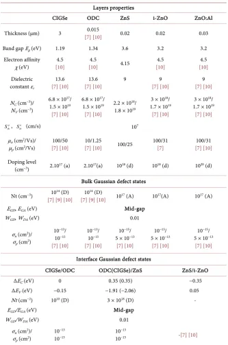
Table 1. Input parameters used for the solar cell simulation. (a) and (d) denote shallow
acceptor and donor while (A)and (D) denote deep acceptor and donor.
Layers properties
CIGSe ODC ZnS i-ZnO ZnO:Al
Thickness (μm) 3 [7] [10] 0.015 0.02 0.02 0.03
Band gap Eg (eV) 1.19 1.34 3.6 3.2 3.2
Electron affinity
χ (eV) [10] 4.5 [10] 4.5 4.15 [10] 4.5 [10] 4.5
Dielectric constant εr
13.6
[7] [10] [7] [10] 13.6 9 [7] [10] 9 [7] [10] 9
NC (cm−3)/
NV (cm−3)
6.8 × 10¹⁷/
1.5 × 10¹⁹
[7] [10]
6.8 × 10¹⁷/
1.5 × 10¹⁹
[7] [10]
2.2 × 10¹⁸/
1.8 × 10¹⁹
3 × 10¹⁸/
1.7 × 10¹⁹
[7] [10]
3 × 10¹⁸/
1.7 × 10¹⁹
[7] [10]
p th
S , n
th
S (cm/s) 107
μn (cm2/Vs)/
μp (cm2/Vs)
100/50
[7] [10] [7] [10] 10/1.25 100/25 100/31 [7] [7] [10] 100/31
Doping level
(cm−3) 2.1017 (a) 2.1017(a) 1018 (d) 1018 (d) 1020 (d)
Bulk Gaussian defect states
Nt (cm−3) 1014 (D)
[7] [9] [10] 10
14 (D)
[7] [9] [10] 1017 (A) 1017(A) 1017 (A)
EGD, EGA (eV) Mid-gap
WGD, WDA (eV) 0.01
σn (cm2)/
σp (cm2)
10−13/
10−15
[7] [10]
10−13/
10−15
[7] [10]
10−15/
5 × 10⁻¹³
[7] [10]
10−15/
5 × 10⁻¹³
[7] [10]
10−15/
5 × 10⁻¹³
[7] [10]
Interface Gaussian defect states
CIGSe/ODC ODC(CIGSe)/ZnS ZnS/i-ZnO
ΔEC (eV) 0 0.35 (0.35) −0.35
ΔEV (eV) −0.15 −1.91 (−2.06) 0.05
Nt (cm−2) 1010 (D) 3 × 10¹⁸ (D) -
EGD/EGA (eV) Mid-gap
WGD/WDA (eV) 0.01
σn (cm2)/
σp (cm2)
10−13
10−15 10
−13
10−15 -[7] [10]
2. Description of the Solar Cell Model
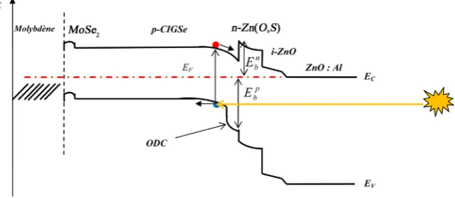
In the present study the CIGS cell structure is consisted of seven stacked layers including the top and back contacts. The CIGS-based solar cell schematic ener-gy-band diagram is illustrated in Figure 1. Based on previous work [9][10][11] [12] the contacts are assumed ohmic with surface recombination velocities
7
10 cm s
n p
DOI: 10.4236/ojmsi.2017.54016 221 Open Journal of Modelling and Simulation
Figure 1. Band diagram of CIGS-based solar cells.
buffer layers. This layer is considered to improve the CIGS cells performance because it increases the absorber band gap at the buffer-absorber interface by lowering the valence band maximum with respect to the Fermi level, and hence reduces the interface recombination rate. Several models have been proposed to explain the properties of this inverted CIGS absorber surface [13]-[25]: the dop-ing model of n-type ODC and the Fermi level pinndop-ing model. For our cell, we used the Fermi level pinning model, characterized by a high density, (3 × 1018 cm−3) of donor defects located at 0.2 eV below the CIGS absorber conduction band. These defects have small capture cross-sections, 18 2
10 cm
n p
σ =σ = − , to
separate pinning defects from recombination defects of SDL. In our simulations, we considered two deep Gaussian defect distributions with narrow bandwidths: donor defects are assigned to the p-type materials and acceptor defects to then-type materials. The bulk recombination defect states are positioned at mid gap of the re-spective layers and the interface defects are placed at the mid gap of the lowest band gap of the two adjacent materials, except for buffer-absorber interface donor defects.
The Shockley-Read-Hall model is used within AFORS-HET to describe the recombination currents in bulk levels and the defects at the interface. The cur-rent transport across interfaces is describes by drift-diffusion approximation and the front and backside boundaries of the semiconductor stack are described by the flat band metal/semiconductor contact model.
The photon absorption is calculated from the spectral absorption coefficient
( )
4πk( )
λ α λλ
= (2)
of each semiconductor layer within the stack and α(λ) has been calculated from the extinction coefficient k(λ) measured by [26][27][28][29].
3. Numerical Simulation
identi-DOI: 10.4236/ojmsi.2017.54016 222 Open Journal of Modelling and Simulation fication of the most important parameters which influence the performance of solar cells and also provides a good understanding their operation since com-plete devices can now be computationally fabricated, simulated and optimized. Several software packages, among which SCAPS-1D (Solar Cell Capacitance Si-mulator One dimension), ASA (Amorphous Semiconductor Analysis), PC1-D (Personal Computer One Dimension), AMPS-1D (Analysis of Micro-electronic and Photonic Structures) and AFORS-HET (Automat FOR Simulation for HE-Terostructures) have been developed to simulate the operation of thin-film solar cells. The advantage of these computer programs is that parameters can be mod-ified on demand, out of the constraints imposed by technological fabrication processes, to simulate relevant mechanisms and provide a clear understanding of the physics of these devices. In this work the powerful numerical simulation tool, AFORS-HET, is used by specifying the parameters listed in Table 1 as inputs. Using Shockley-Read-Hall recombination model, the software numerically solves the one dimensional equations: Poisson’s equation and the transport and continuity equations for electrons and holes, governing the semiconductor ma-terial under steady-state conditions, and calculates their basic characteristics, such as band diagram, generation and recombination rates, carrier densities and cell currents [30]. The cell is subjected to AM1.5G solar spectrum with an inci-dent power density of 100 mW/cm2 at room temperature. The Air Mass (AM) quantifies the reduction in the power of light as it passes through the atmosphere and is absorbed by air and dust. The standard spectrum at the Earth’s surface is called AM1.5G, (the G stands for global and includes both direct and diffuse radia-tion). The standard AM1.5G spectrum has been normalized to give 100mW/cm2.
We first do not take the effects of reflection on the front and back surfaces, se-ries resistance and shunt resistance into account. For comparison purposes, we first calculate the performances of a n-ZnO:Al/i-ZnO/n-ZnS/p-CIGS/Mo solar cell with our reference parameters corresponding to the same structure with a CdS buffer layer. Figure 2(a) is a plot of the resulting J-V characteristic, with emphasis on the particular values of short circuit current JSC, open circuit voltage
VOC, fill factor FF and conversion efficiency η, extracted from the J-V curve.
Figure 2(b) shows the external quantum efficiency EQE as a function of the wavelength of the incident light.
4. Results and Discussion
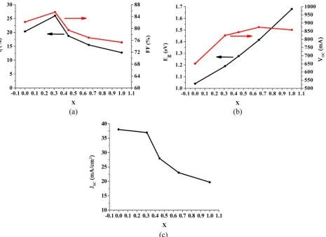
4.1. Effect of Ga-Content of Absorber Layer
DOI: 10.4236/ojmsi.2017.54016 223 Open Journal of Modelling and Simulation
Figure 2. (a) Current density vs. voltage; and (b) external quantum efficiency of the solar cell.
Figure 3. Characteristic parameters of the solar cell as function of the Ga-content: (a) conversion efficiency and fill factor; (b)
CIGS band gap and open circuit voltage; (c) short circuit current.
For this reason, we only observe a slight decrease of the conversion efficiency for
DOI: 10.4236/ojmsi.2017.54016 224 Open Journal of Modelling and Simulation layer which has a minimum value around 1015 cm−3, according to G. Hanna etal.
[33]. The fill factor follows the same trend as the conversion efficiency, although its variations do not exceed 10%. As expected, JSC decreases and VOC increases with x, e.g. the absorber band gap, resulting from a simultaneous reduction of the photo-generation rate and the carrier recombination rate [34]. However, looking into more details, Eg and VOC show opposite curvatures (see Figure
3(b)). To explain this feature, let us remind that the carrier recombination rate depends upon two parameters: 1) the intrinsic carrier concentration, an expo-nential function of the band gap; and 2) the carrier lifetime. The first term un-derlines the strong relation between VOC and Eg. The difference in curvatures is related to the second term and clearly expresses a decrease of the carrier lifetime with increasing band gap. The carrier lifetime decrease is related to the bulk de-fect concentrations which first decrease from 5 × 1015 cm−3 to 1015 cm−3 with in-creasing Ga-content and increase again to 5 × 1016 cm−3 at x = 1 [33]. In conclu-sion, the optimum Ga-content is equal to 0.31 and is very close to values re-ported in literature [25][33][35].
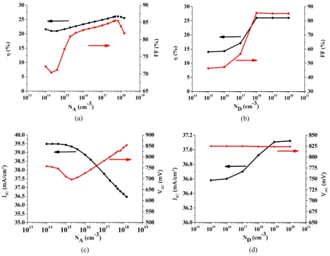
4.2. Effects of Absorber and Buffer Doping Concentrations
In this section we successively investigate the effects of the doping levels of the absorber and the defect layers on the CIGS solar cell performances. All electrical properties of the layers are chosen similar to the bulk CIGS, except the energy band gap and the carrier mobilities (see Table 1). Figure 4 represents the varia-tions of the solar cell characteristic parameters versus absorber and buffer dop-ing concentrations. Let us remind that the absorber layer is of p-type and the buffer layer of n-type. It has been reported [7] that when the absorber doping is above 1017 cm−3 or when the buffer layer doping is below 1018 cm−3 the conduc-tion band minimum shift with respect to Fermi level is very high. This means that the Fermi level is no longer pinned and the buffer-absorber interface re-combination becomes important. When the buffer layer doping is equal to 1018 cm−3 and the absorber doping is below 1017 cm−3 the Fermi level is pinned. The solar cell performance is then governed by the bulk recombination properties of the absorber layer. This behavior is seen in Figure 4(a) where both the conver-sion efficiency and FF show an optimum at a doping level of 5 × 1017 cm−3 How-ever, the sensitivity to the absorber doping level is not strong and limited to few percent. Finally, we observe that JSC and FF show only slight variation for all ab-sorber doping levels above 1017 cm−3. Here, the limiting characteristic is V
OC which is degraded at low absorber doping levels, reducing the conversion effi-ciency of the solar cell.
Keeping the absorber layer doping at 5 × 1017 cm−3, Figure 4(b) and Figure
DOI: 10.4236/ojmsi.2017.54016 225 Open Journal of Modelling and Simulation
Figure 4. Characteristic parameters of the solar cell as a function of the carrier concentration in the absorber and buffer layers: (a),
(b) conversion efficiency and fill factor; (c), (d) short circuit current and open circuit voltage. NA is the acceptor concentration in
CIGS layer and ND the donor concentration in ZnS layer.
4.3. Effect of Buffer Layer Thickness
DOI: 10.4236/ojmsi.2017.54016 226 Open Journal of Modelling and Simulation
Figure 5. Characteristic parameters of the solar cell as a function of ZnS buffer layer
thickness: (a) conversion efficiency and fill factor; (b) short circuit current and open cir-cuit voltage.
Figure 6. External quantum efficiency of the solar cell for different
thicknesses of ZnS buffer layer.
in this narrow range is at the origin of the JSC decrease for thicknesses over 30 nm, leading to a small loss of efficiency. In conclusion, the buffer layer optimal thickness of 30 nm should merely be considered as an indication, to be com-bined with other technological considerations, rather than a mandatory value to be strictly respected.
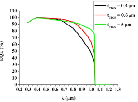
4.4. Effect of Absorber Layer Thickness
Contrary to ZnS, the CIGS layer acts as the absorber, necessitating the use of rel-atively thick layers. Setting the buffer layer thickness to 30 nm, we represent in
[image:9.595.251.498.276.442.2]DOI: 10.4236/ojmsi.2017.54016 227 Open Journal of Modelling and Simulation
Figure 7. Characteristic parameters of solar cell as a function of CIGS absorber layer
thickness: (a) conversion efficiency and fill factor; (b) short circuit current and open cir-cuit voltage.
Figure 8. External quantum efficiency of the solar cell for
dif-ferent thicknesses of CIGS absorber layer.
appreciably with the thickness, at wavelengths above 0.6 μm. However, for thicknesses beyond 5 μm, the quantum efficiency remains almost unchanged at all wavelengths above the CIGS band gap: we have reached the maximum pho-ton absorption.
Looking now at VOC in Figure 7(b), we observe a decrease of VOC with in-creasing thickness, due to the increase of the bulk recombination rate. FF is al-most constant over the whole range. For thicknesses above 1 μm, the interesting effect is that the simultaneous increase of JSC and decrease of VOC compensate each other so that the conversion efficiency is hardly affected. As a result, as far as the absorber thickness exceeds 1 μm, other technological or economic con-siderations should also be taken into account. Materials cost and availability, concerning indium in particular are of primary importance. The best compro-mise is a CIGS absorber thickness of 3 μm corresponding to a conversion effi-ciency of 26%.
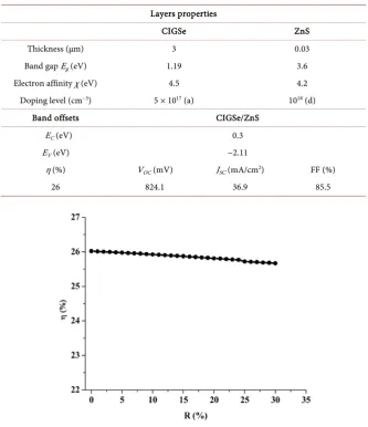
[image:10.595.262.490.268.436.2]perfor-DOI: 10.4236/ojmsi.2017.54016 228 Open Journal of Modelling and Simulation mances.
The reflection can easily be taken into account (anti-reflection layer) by mod-ifying the spectral amplitude of the spectrum used on the illuminated front side. The effect of the front side reflection has been investigated on the solar cell per-formances. Figure 9 represents the variation of the efficiency versus the reflec-tion coefficient. The figure shows that the efficiency decreases almost linearly when the reflection coefficient increases, although its decrease does not exceed 0.35% when the reflection coefficient reaches 30%. A large reduction of optical losses can be achieved by using a transparent anti-reflet layer which allows better photon transmission to the absorber.
5. Conclusion
[image:11.595.206.540.311.698.2]In this work, the numerical modeling software AFOERS-HET was used to simu-late a CIGS-based solar cell operating under AM.1.5G solar spectrum at room
Table 2. Optimum values of the parameters in CIGS solar cells with ZnS buffer layers.
Layers properties
CIGSe ZnS
Thickness (μm) 3 0.03
Band gap Eg (eV) 1.19 3.6
Electron affinity χ (eV) 4.5 4.2
Doping level (cm−3) 5 × 10¹⁷ (a) 1018 (d)
Band offsets CIGSe/ZnS
EC (eV) 0.3
EV (eV) −2.11
η (%) VOC (mV) JSC (mA/cm2) FF (%)
[image:11.595.205.542.317.699.2]26 824.1 36.9 85.5
Figure 9. Efficiency of the CIGS/ZnS solar cell versus the
DOI: 10.4236/ojmsi.2017.54016 229 Open Journal of Modelling and Simulation ers. Simulations give optimum thicknesses of 30 nm for the buffer layer and 3 μm for the absorber layer. Finally, calculating the quantum efficiency, we show how an increase of the buffer layer thickness degrades the solar cell perfor-mances while an increase of the absorber layer thickness improves the solar cell efficiency.
References
[1] Wei, S.-H., Zhang, S.B. and Zunger, A. (1998) Effects of Ga Addition to CuInSe2 on
Its Electronic, Structural, and Defect Properties. Applied Physics Letters, 72, 3199. https://doi.org/10.1063/1.121548
[2] Huang, C.H. (2008) Effects of Ga Content on Cu(In,Ga)Se2 Solar Cells Studied by
Numerical Modelling. Journal of Physics and Chemistry of Solids, 69, 330-334. https://doi.org/10.1016/j.jpcs.2007.07.093
[3] Green, M.A., Hishikawa, Y., Warta, W., Dunlop, E., Levi, D., Hohl-Ebinger, J. and Ho-Baillie, A.W.H. (2017) Solar Cell Efficiency Tables (Version 50). Progress in Photovoltaics, 25, 668-676. https://doi.org/10.1002/pip.2909
[4] Pianezzi, F., Reinhard, P., Chiril, A., Nishiwaki, S., Bissig, B., Buecheler, S. and Ti-wari, A.N. (2013) Defect Formation in Cu(In,Ga)Se2 Thin Films Due to the
Pres-ence of Potassium during Growth by Low Temperature Co-Evaporation Process.
Journal of Applied Physics, 114, Article ID: 194508.
https://doi.org/10.1063/1.4832781
[5] Pohl, J. and Albe, K. (2013) Intrinsic Point Defects in CuInSe2 and CuGaSe2 as Seen
via Screened-Exchange Hybrid Density Functional Theory. Physical Review B, 87, Article ID: 245203.https://doi.org/10.1103/PhysRevB.87.245203
[6] Ahn, B.T., Larina, L., Kim, K.H. and Ahn, S.J. (2008) Development of New Buffer Layers for Cu(In,Ga)Se2 Solar Cells. Pure and Applied Chemistry, 80, 2091-2102.
https://doi.org/10.1351/pac200880102091
[7] Pettersson. J. (2012) Modeling Band Gap Gradients and Cd-Free Buffer Layers in
Cu(In,Ga)Se2 Soalr Cells. Ph.D. Thesis, Uppsala University, Uppsala.
[8] Meyer, B.K., Polity, A., Farangis, B., He, Y., Hasselkamp, D., Krämer, Th. and Wang, C. (2004) Structural Properties and Band Gap Bowing of ZnO1-xSx Thin
Films Deposited by Reactive Sputtering. Applied Physics Letters, 85, 4929-4931. https://doi.org/10.1063/1.1825053
[9] Gloeckler, M., Fahrenbruch, A.L. and Sites, J.R. (2003) Numerical Modeling of CIGS and CdTe Solar Cells: Setting the Baseline. 3rd World Conference of Photo-voltaic Energy Conversion, Osaka, 11-18 May 2003.
DOI: 10.4236/ojmsi.2017.54016 230 Open Journal of Modelling and Simulation
Based Solar Cells. Thin Solid Films, 480-481, 433-438. https://doi.org/10.1016/j.tsf.2004.11.098
[11] Kohara, N., Nishiwaki, S., Hashimoto, Y., Negami, T. and Wada, T. (2001) Electri-cal Properties of the Cu(In,Ga)Se2/MoSe2/Mo Structure. Solar Energy Materials & Solar Cells, 67, 209-215.
[12] Wurz, R., Fuertes Marron, D., Meeder, A., Rumberg, A., Babu, S.M., Schedel Nie-drig, T., Bloeck, U., Schubert-Bischoff, P. and Lux-Steiner, M.C. (2003) Formation of an Interfacial MoSe2 Layer in CVD Grown CuGaSe2 Based Thin Film Solar Cells. Thin Solid Films, 431-432, 398-402.
[13] Yan, Y., Jones, K. M., Abushama, J., Young, M., Asher, S., Al-Jassim, M.M. and Noufi, R. (2002) Microstructure of Surface Layers in Cu(In,Ga)Se2 Thin Films. Ap-plied Physics Letters, 81, 1008.https://doi.org/10.1063/1.1498499
[14] Herberholz, R., Rau, U., Schock, H.W., Haalboom, T., Gödecke, T., Ernst, F., Beil-harz, C., Benz, K.W. and Cahen, D. (1999) Phase Segregation, Cu Migration and
Junction Formation in Cu(In, Ga)Se2. The European Physical Journal Applied
Physics, 6, 131.https://doi.org/10.1051/epjap:1999162
[15] Zhang, S.B., Wei, S.-H., Zunger, A. and Yoshida, H.K. (1998) Defect Physics of the CuInSe2 Chalcopyrite Semiconductor. Physical Review B, 57, 9642.
https://doi.org/10.1103/PhysRevB.57.9642
[16] Schmid, D., Ruckh, M., Grunwald, F. and Schock, H.W. (1993) Chalcopyrite/Defect Chalcopyrite Heterojunctions on the Basis of CuInSe2. Journal of Applied Physics,
73, 2902.
[17] Schmid, D., Ruckh, M. and Werner Schock, H. (1996) A Comprehensive
Charac-terization of the Interfaces in Mo/CIS/CdS/ZnO Solar Cell Structures. Solar Energy Material and Solar Cells, 41-42, 281-294.
[18] Li, Z., Nishijima, M., Yamada, A. and Konagai, M. (2009) Growth of Cu(In,Ga)Se2
Thin Films using Ionization Ga Source and Application for Solar Cells. Physica Status Solidi, 6, 1273-1277.https://doi.org/10.1002/pssc.200881180
[19] Zunger, A., Zhang, S.B. and Wei, S.-H. (1998) Revisiting the Defect Physics in Cu-InSe2 and CuGaSe2. In: Basore, P.A. (Ed.), Proceedings of the 26th IEEE PV Special-ist Conference, AIP, New York, 313.
[20] Levcenko, S., Durán, L., Gurieva, G., Alonso, M.I., Arushanov, E., Durante Rincón, C.A. and León, M. (2010) Optical Constants of Cu(In1−xGax)5Se8 Crystals. Journal of Applied Physics, 107, Article ID: 033502.https://doi.org/10.1063/1.3298499
[21] Zhao, H., Kumar, M. and Persson, C. (2012) Density Functional Theory Study of
Ordered Defect Cu-(In,Ga)-Se Compounds. Physica Status Solidi, 9, 1600-1603. https://doi.org/10.1002/pssc.201100671
[22] Kwon, S.H., Park, S.C., Ahn, B.T., Yoon, K.H. and Song, J. (1998) Effect of CuIn3Se5
Layer Thickness on CuInSe2 Thin Films and Devices. Solar Energy,64, 55-60.
[23] Dharmadasa, I.M. (2009) Fermi Level Pinning and Effects on CuInGaSe2-Based
Thin-Film Solar Cells. Semiconductor Science and Technology, 24, Article ID: 055016.
[24] Jaffe, J.E. and Zunger, A. (1984) Theory of the Band-Gap Anomaly in ABC2
Chal-copyrite Semiconductors. Physical Review B, 29, 1882-1906.
[25] Huang, C.-H. (2008) Effects of Junction Parameters on Cu(In,Ga)Se2 Solar Cells. Journal of Physics and Chemistry of Solids, 69, 779-783.
DOI: 10.4236/ojmsi.2017.54016 231 Open Journal of Modelling and Simulation
(2002) Optical Functions of Chalcopyrite CuGaxIn1−xSe2 Alloys. Applied Physics A,
74, 659-664.https://doi.org/10.1007/s003390100931 [30] Simulation of Heterojunction Solar Cells with AFORS-HET.
http://shodhganga.inflibnet.ac.in/bitstream/10603/42510/8/09_chapter%204.pdf [31] Huang, C.-H. (2008) Effects of Ga Content on Cu(In,Ga)Se2 Solar Cells Studied by
Numerical Modeling. Journal of Physics and Chemistry of Solids, 69, 330-334. [32] Wei, S.-H. and Zunger, A. (1995) Band Offsets and Optical Bowings of
Chalcopyri-tes and Zn-Based II-VI Alloys. Journal of Applied Physics, 78, 3846-3856.
https://doi.org/10.1063/1.359901
[33] Hanna, G., Jasenek, A., Rau, U. and Schock, H.W. (2001) Influence of Ga-Content on the Bulk Defect Densities of Cu(In,Ga)Se2. Thin Solid Films, 387, 71-73.
[34] Touafek, N. and Mahamdi, R. (2014) Back Surface Recombination Effect on the Ul-tra-Thin CIGS Solar Cells by SCAPS. International Journal of Renewable Energy Research, 4, 958-964.