Technische Universität Dresden
Electrical Characterisation of
Ferroelectric Field Effect Transistors based on
Ferroelectric HfO
2Thin Films
Dipl.-Ing. Ekaterina Yurchuk
von der Fakultät Elektrotechnik und Informationstechnik der
Technischen Universität Dresden
zur Erlangung des akademischen Grades
Doktoringenieur
(Dr.-Ing.)
genehmigte Dissertation
Vorsitzender: Prof. Dr.-Ing. habil. R. Schüffny
Gutachter: Prof. Dr.-Ing. T. Mikolajick Tag der Einreichung: 23.07.2014 Prof. Dr. K. Dörr Tag der Verteidigung: 06.02.2015
Abstract
The ferroelectric field effect transistors (FeFETs) are considered as promising candidates for future non-volatile memory applications due to their attractive features, such as non-volatile data storage, program/erase times in the range of nanoseconds, low operation voltages, almost unlimited endurance, non-destructive read-out and a compact one-transistor cell structure without any additional access device needed. Despite the efforts of many research groups an industrial implementation of the FeFET concept is still missing. The main obstacles originate from the conventional perovskite ferroelectric materials (lead zirconium titanate (PZT) and strontium bismuth tantalate (SBT)), in particular their integration and scaling issues. The recently discovered ferroelectric behaviour of HfO2-based dielectrics
yields the potential to overcome these limitations. The decisive advantages of these materials are their full compatibility with the standard CMOS process and improved scaling potential. Utilisation of the Si:HfO2 ferroelectric thin films allows to fabricate FeFETs in a
state-of-the-art CMOS technology node of 28 nm. The ferroelectricity in HfO2 has been discovered only
several years ago. Therefore, there are still a lot of uncertainties about the origin of the ferroelectric behaviour as well as the impact of different fabrication conditions on its emergence. Moreover, the electrical behaviour of both the HfO2-basedferroelectric films and
memory devices based on these films requires more detailed studies. The emphasis of this work lays on the ferroelectric properties of HfO2 thin films doped withsilicon (Si:HfO2). The
potential and possible limitations of this material with the respect to the application in non-volatile FeFET-type memories were extensively examined.
The material aspects of the Si-doped HfO2 thin films were studied at first in order to
gain better insight into the occurrence of ferroelectricity in this system and to acquire guidelines for FeFET fabrication. The influence of the different process parameters such as the Si doping concentration, post-metallisation annealing conditions and film thickness on the stabilisation of the ferroelectric properties in Si:HfO2 films has been examined. Electrical
characterisation combined with structural analyses enabled the correlation of the changes in the macroscopic electrical properties to alterations in the film crystalline structure. The film composition was shown to have a strong impact on the electrical properties of Si:HfO2 films.
By varying the silicon doping level, paraelectric, ferroelectric or antiferroelectric-like behaviour was induced. Moreover, the temperature of the post-metallisation annealing as well as the film thickness can be used to tune the ferroelectric properties of the Si:HfO2 films by
Furthermore, the electrical behaviour of the ferroelectric Si:HfO2 films was analysed in
detail. The effect of field cycling, polarisation switching kinetics and ferroelectric specific degradation (fatigue) were investigated. The improvement of the ferroelectric properties upon field cycling (“wake up” effect) that is often observed in perovskite ferroelectrics was also detected for Si:HfO2 ferroelectric films. The polarisation switching times in the nanosecond
range were ascertained. Fatigue properties of Si:HfO2 films were shown to depend on the
frequency and voltage amplitude. In contrast to perovskite ferroelectrics a dielectric breakdown was identified as one of the factors that limited the cycling capability of the Si:HfO2 ferroelectrics. Due to operation at MHz frequencies and electric fields below
3 MV/cm the cycling capability was extended to 109 cycles and a fatigue-free behaviour was demonstrated up to 106 cycles.
The performance of the Si:HfO2-based MFIS-FET devices, which were fabricated using
the state-of-the-art 28 nm high-k metal gate CMOS technology, was investigated including the key memory characteristics, such as the program and erase behaviour, retention and endurance. The studied FeFETs demonstrated program and erase times in the nanosecond regime (10 – 100 ns) with operation voltages of 4 – 6 V. The operation capability of the Si:HfO2-based ferroelectric transistors was proven in the temperature range between 25 and
210 °C. The retention behaviour of the studied devices deteriorated with increasing temperature and improved at higher operation voltages. Furthermore the impact of scaling on the memory performance of Si:HfO2-based MFIS-FETs down to the gate length of 28 nm was
investigated. The scaled devices demonstrated memory characteristics comparable to that of the long channel structures. The transistor short channel effect rather than deteriorated ferroelectric properties explained the observed difference in the behaviour of the scaled devices in comparison to the long channel devices.
The endurance (limited to 104 – 105 program/erase cycles) and charge trapping that is superimposed with the ferroelectric switching were identified as the main issues of the Si:HfO2-based FeFET devices. A detailed study of both these issues was performed in this
work. The limited endurance was found to be linked to the reliability of the transistor gate stack. A predominant degradation of the interfacial layer, which is embedded between the silicon substrate and the ferroelectric film, was detected. This was similar to the behaviour of the standard high-k metal gate stacks. Indications that this process can be held responsible for the endurance behaviour of the Si:HfO2-based MFIS-FET devices were discussed. The
electron trapping enhanced by the ferroelectric polarisation charge was shown to superimpose with the ferroelectric switching at typical erase operation conditions. This electron trapping impaired a fast erase. It is also suggested as the main cause of the interfacial layer degradation upon endurance cycling. A modified approach for the erase operation was proposed in this work in order to mitigate the impact of trapping and increase the effective erase speed.
Kurzzusammenfassung
Die ferroelektrischen Feldeffekttransistoren (FeFETs) zählen mit zu den vielversprechenden Kandidaten für zukünftige nichtflüchtige Speicheranwendungen. Der Grund dafür sind ihre attraktiven elektrischen Eigenschaften: die nichtflüchtige Datenspeicherung, Programmier- und Löschzeiten im Bereich von wenigen Nanosekunden, niedrige Betriebsspannungen, nahezu unbegrenzte Zyklenfestigkeit, nichtzerstörender Lesevorgang und eine kompakte Bauform der Speicherzelle, welche nur aus einem Transistor besteht und keine zusätzliche Zugriffsbauelemente benötigt. Trotz der Bemühungen von vielen Forschungsgruppen, konnte eine industrielle Umsetzung des FeFET-Konzeptes bisher nicht erreicht werden. Die Integrationsschwierigkeiten und Skalierungslimitierungen, die mit den klassischen Perowskit-Ferroelektrika (Blei-Zirkonium-Titanat (PZT) und Strontium-Wismut-Tantalat (SBT)) verbunden sind, sind dafür verantwortlich. Die vor kurzem nachgewiesene Ferroelektrizität von HfO2-basierten Dielektrika bietet das Potenzial diese
Einschränkungen zu überwinden. Der entscheidende Vorteil dieser neuen ferroelektrischen Materialien ist ihre Kompatibilität mit dem CMOS-Prozess in Kombination mit einem besseren Skalierungspotenzial. Die Anwendung von ferroelektrischen Si:HfO2 Dünnschichten
ermöglichte die Herstellung von FeFET Bauelementen auf einem aktuellen CMOS Technologieknoten von 28 nm. Die Entdeckung der ferroelektrischen Eigenschaften in HfO2
Dünnschichten erfolgte erst vor wenigen Jahren. Infolgedessen gibt es immer noch sehr viele Unklarheiten über den genauen Ursprung dieser Eigenschaften und den Einfluss der verschiedenen Herstellungsprozessfaktoren auf ihrer Entstehung. Darüber hinaus muss ein besseres Verständnis vom elektrischen Verhalten, sowohl der HfO2 ferroelektrischen
Dünnschichten, als auch der auf ihnen basierenden Speicherelemente erworben werden. Das elektrische Verhalten von HfO2 Dünnschichten, deren ferroelektrischen Eigenschaften mit
Siliziumdotierung induziert wurden, stellte den Schwerpunkt der vorliegenden Arbeit dar. Das Potenzial und die möglichen Einschränkungen dieses Materialsystems, mit Bezug auf die Anwendung in nichtflüchtigen FeFET Speicherelementen, wurden ausführlich untersucht.
Als Erstes wurden die Materialaspekte der mit Si dotierten HfO2 Dünnschichten mit
dem Ziel analysiert, ein besseres Verständnis für das Auftreten von Ferroelektrizität in diesem System zu gewinnen. Die erworbenen Erkenntnisse dienten später als Leitpfaden für die Herstellung von FeFET Bauelementen. Der Einfluss von verschiedenen
Siliziumdotierung, die Bedingungen für die Postmetallisierungstemperung und die Schichtdicke betrachtet. Die Kombination der elektrischen Charakterisierung mit den Strukturanalysen, ermöglichte die Änderungen in den makroskopischen elektrischen Eigenschaften mit den Änderungen in der Kristallstruktur zu korrelieren. Eine starke Abhängigkeit der elektrischen Schichteigenschaften von deren Zusammensetzung wurde beobachtet. Paraelektrisches, ferroelektrisches und antiferroelektrishes Verhalten konnte durch die Variierung der Siliziumdotierung induziert werden. Darüber hinaus wurden die Temperatur der Postmetallisierungstemperung und die Schichtdicke als zusätzliche Faktoren, die die Phasenzusammensetzung der Si:HfO2 Dünnschichten und als Folge ihre
ferroelektrischen Eigenschaften beeinflussen können, identifiziert.
Im nächsten Schritt wurde eine detaillierte Untersuchung der elektrischen Eigenschaften von den ferroelektrischen Si:HfO2 Dünnschichten durchgeführt. Der Effekt des Feldzyklens,
die Kinetik des Polarisationsschaltvorgangs und die Degradation, verursacht durch ein kontinuierliches Polarisationsschalten (Fatigue), wurden dabei analysiert. Ein elektrisches Wechselfeld verursachte eine Verbesserung der ferroelektrischen Eigenschaften von Si:HfO2
ferroelektrischen Schichten. Dieser sogenannte "wake up"-Effekt ist auch charakteristisch für die klassischen Ferroelektrika. Polarisationsschaltzeiten im Nanosekundenbereich konnten für die untersuchten Si:HfO2 Schichten nachgewiesen werden. Ihre Fatigue-Eigenschaften waren
sehr stark von der Testfrequenz und der Amplitude des Stresssignals abhängig. Im Unterschied zu den klassischen Perowskit-Ferroelektrika, deren Zyklenfestigkeit hauptsächlich durch die Abnahme der schaltbaren Polarisation beeinträchtigt wird, hat sich für die Si:HfO2 ferroelektrischen Schichten der dielektrische Durchbruch als
Hauptlimitierungsfaktor erwiesen. Durch die Anwendung von Frequenzen im MHz-Bereich und elektrischen Feldern unter 3 MV/cm konnte die Zyklenfestigkeit von Si:HfO2 verbessert
werden, so dass 109 Schaltzyklen realisiert werden konnten. Eine nur geringfügige Degradation bei bis zu 106 Zyklen wurde festgestellt.
Die auf Si:HfO2 Dünnschichten basierenden FeFET Speicherelemente wurden auf der
Basis eines High-k-Metall-Gate-CMOS Prozesses im 28 nm Technologieknoten hergestellt. Ihre wichtigsten Betriebseigenschaften einschließlich der Datenhaltung, der Zyklenfestigkeit, des Programmier- und Löschverhaltens wurden untersucht. Die Programmier- und Löschzeiten im Nanosekunden-Zeitregime (10 – 100 ns) mit Betriebsspannungen von 4 – 6 V konnten nachgewiesen werden. Darüber hinaus wurde die Funktionsfähigkeit dieser Speicherelemente in einem Temperaturbereich von 25 bis 210 °C getestet. Mit zunehmender Temperatur wurde eine Verschlechterung der Datenhaltungseigenschaften festgestellt. Die höheren Betriebsspannungen hatten einen entgegengesetzten Effekt und bewirkten eine Verbesserung der Datenhaltung. Zusätzlich wurde der Einfluss der Skalierung auf die Funktionalität der auf Si:HfO2-basierenden FeFETs analysiert. Zu diesem Zweck wurden die
Speicherelemente mit Gatelängen bis zu 28 nm hergestellt. Die hochskalierten ferroelektrischen Transistoren zeigten vergleichbare Charakteristiken zu den Langkanaltransistoren. Die Unterschiede in dem Verhalten zwischen Speicherelementen mit kurzen und langen Kanälen konnten größtenteils durch Transistorkurzkanaleffekte erklärt werden. Im Gegensatz dazu waren die ferroelektrischen Eigenschaften von der Skalierung nur geringfügig beeinflusst.
Die Hauptproblemen von auf Si:HfO2 basierenden FeFET Speicherelementen sind zum
heutigen Zeitpunkt die Zyklenfestigkeit (begrenzt auf 104 – 105 Programmier- und Löschzyklen) und der Ladungseinfang, der sich mit dem ferroelektrischen Schalten überlagert. In der vorliegenden Arbeit wurde eine ausführliche Analyse beider Aspekte durchgeführt. Es wurde festgestellt, dass Eigenschaften des Transistorgatestapels hauptsächlich für die limitierte Zyklenfestigkeit verantwortlich sind. Eine Ähnlichkeit zwischen den Degradationsvorgängen im ferroelektrischen und dem hoch- Gatestapel wurde festgestellt. Die Degradation während des kontinuierlichen Programmierens und Löschens beschränkte sich auf die Grenzschicht zwischen Substrat und hoch- Dielektrikum. Die Verschlechterung der Speichereigenschaften in den HfO2-basierten FeFETs beim
Programmieren und Löschen lässt sich durch die Gatestapeldegradation erklären. Ein weiterer Einflussfaktor ist der Elektroneneinfang während des Löschens, der durch die ferroelektrische Polarisation des Gatestapels zusätzlich verstärkt wird. Das hat zur Folge, dass sich die Elektroneninjektion vom Halbleitersubstrat bei typischen Löschbedingungen mit dem ferroelektrischen Schalten überlagert. Das gleichzeitige Einfangen von Elektronen beim Schalten, wirkt sich nachteilig auf die Löschgeschwindigkeit aus, die sich dramatisch reduziert. Das Einfangen von Elektronen wurde auch für die Degradation des Transistorstapels während des Zyklens und somit für die begrenzte Zyklenfestigkeit der ferroelektrischen Transistoren verantwortlich gemacht. Ein modifizierter Ansatz für die Löschoperation mit dem Ziel den schädlichen Effekt des Elektroneinfangs zu reduzieren und die effektive Löschgeschwindigkeit zu verbessern wurde in dieser Arbeit vorgeschlagen.
Contents
1
Introduction ... 1
2
Fundamentals ... 5
2.1 Non-volatile semiconductor memories ... 5
2.2 Emerging memory concepts ... 10
2.3 Ferroelectric memories ... 14
3
Characterisation methods ... 29
3.1 Memory characterisation tests ... 29
3.2 Ferroelectric memory specific characterisation tests ... 32
3.3 Trapping characterisation methods ... 38
3.4 Microstructural analyses ... 44
4
Sample description ... 49
4.1 Metal-insulator-metal capacitors ... 49
4.2 Ferroelectric field effect transistors ... 50
5
Stabilisation of the ferroelectric properties in Si:HfO
2thin films ... 53
5.1 Impact of the silicon doping ... 54
5.2 Impact of the post-metallisation anneal ... 64
5.3 Impact of the film thickness ... 67
5.4 Summary ... 72
6
Electrical properties of the ferroelectric Si:HfO
2thin films ... 75
6.1 Field cycling effect ... 75
6.2 Switching kinetics ... 78
6.3 Fatigue behaviour ... 80
7
Ferroelectric field effect transistors based on Si:HfO
2films ... 87
7.1 Effect of the silicon doping ... 88
7.2 Program and erase operation ... 90
7.3 Retention behaviour ... 92
7.4 Endurance properties ... 94
7.5 Impact of scaling on the device performance ... 103
7.6 Summary ... 109
8
Trapping effects in Si:HfO
2-based FeFETs ... 113
8.1 Trapping kinetics of the bulk Si:HfO2 traps ... 114
8.2 Detrapping kinetics of the bulk Si:HfO2 traps ... 117
8.3 Impact of trapping on the FeFET performance ... 119
8.4 Modified approach for erase operation ... 121
8.5 Summary ... 124
9
Summary and Outlook ... 127
Bibliography ... 133
List of symbols and abbreviations ... 157
List of Publications ... 163
1
Introduction
Advancement in the field of microelectronics in the last several decades has revolutionised your daily life, where numerous electronic devices have become its inextricable part. The recent trend is a rapid popularisation of portable electronic devices (smart phones, digital audio players and digital cameras) and portable storage media (memory cards, USB flash drives, solid-state drives). A key enabling technology for this trend is non-volatile semiconductor memories (NVSMs) due to their capability of non-non-volatile data storage, speed, compactness, mechanical robustness and low power consumption [1]. A continuous demand for the higher memory capacity, better performance and more functionality at lower costs drives a continuously ongoing increase in the storage density, which is achieved by scaling of elementary memory devices. The current concept used in NVSMs is the floating-gate (FG) technology, in which the data is stored in form of electric charges within a conductive layer (floating-gate) embedded into a gate stack of a field effect transistor. Up to now the FG devices were able to scale like all silicon technology in accordance with Moore’s law [2], which predicts a doubling of transistor density in an integrated circuit approximately every two-three years. The contemporary technological node for NAND architecture reached the 16 nm benchmark [3], resulting in several billions of transistors on one semiconductor chip. Further scaling will, however, be rather challenging, since the FG approach is already reaching its physical scaling limits [4], [5]. The inability to downsize the thickness of the insulating layers below 6 nm, the resulting high programming voltages, few-electron storage and cross-talk between neighbouring memory cells are the main obstacles for FG downsizing into 1x-nm and below [1], [6], [7]. In addition the FG cell exhibit several other drawbacks such as program/erase times in the range of microseconds to milliseconds, which makes it suitable only as a storage-type memory, as well as significantly higher operation voltages above 15 V in comparison to CMOS logic devices (below 1 V). Therefore, there is a strong demand on new memory concepts, which will be able to overcome the above mentioned limitations of the contemporary technology. The desired features are scaling potential below 16 nm, operation times of several nanoseconds comparable to volatile memories (SRAM and DRAM) in combination with non-volatile data storage possibility as well as low power operation. A wide variety of alternative memory approaches are being recently studied. Charge-trapping memories [8], [9], magnetic RAM [10], phase change RAM [11], resistive RAM [12] and ferroelectric RAM [13] are considered by the International
1 Introduction
In the ferroelectric memories the spontaneous polarisation of the ferroelectric materials is utilised for data storage. This type of memories provides the potential for fast operation due to polarisation switching capability in the nanosecond time range, fast unlimited endurance properties and non-volatile data storage. Moreover, since the ferroelectricity is an intrinsic material property with a single polarisation dipole stored within a unit crystal cell, the scaling can theoretically proceed down to the crystal unit-cell size [14]. The concept of a one-transistor ferroelectric cell (FeFET) is especially promising due to a cell design similar to the floating-gate memory but with a different gate stack structure. It provides the possibility for a destructive readout and a potential for a high integration density. The concept of a non-volatile ferroelectric transistor was proposed in the late 1950’s [15]. Its industrial implementation is, however, still missing. The main obstacles originate from the conventional perovskite-type ferroelectric materials (lead zirconium titanate (PZT) and strontium bismuth tantalate (SBT)), in particular their integration [16], [17] and scaling issues [13]. The recently discovered ferroelectric properties of HfO2-based thin films [18] – [20] renewed the interest in
FeFET [21]. The decisive advantages of the HfO2-based ferroelectrics are their full
compatibility with the standard CMOS process and stable ferroelectric properties at film thicknesses in the nanometre range (5 – 30 nm) [22], [23]. The latter allow for a drastic reduction of the gate stack height, providing gate stack aspect ratios more suitable for scaling. The better scaling potential of HfO2-based ferroelectrics is also assisted by a significantly
lower dielectric constant of ~25 (for PZT or SBT ~200–300) and higher coercive field strength EC of ~1 MV/cm (for PZT or SBT ~50 kV/cm). At reduced ferroelectric thickness
these material properties enable to avoid high depolarization fields and compensate the memory window loss. Utilizing ferroelectric Si:HfO2, FeFETs were fabricated at a
state-of-the-art 28 nm technology node, which finally closed the scaling gap between the ferroelectric and CMOS logic transistors [24]. The effect of the ferroelectricity in HfO2 has been
recognised only several years ago. Therefore, there are still a lot of uncertainties about the origin of this ferroelectric behaviour as well as the impact of different fabrication conditions on its emergence. Moreover, the electrical behaviour of both, the HfO2-based ferroelectric
films and memory devices based on these films, requires more detailed studies.
The emphasis of this work lay on the properties of HfO2 thin films, in which the
ferroelectricity is induced by the silicon doping (Si:HfO2). The potential and possible
limitations of this material system with the respect to the application in non-volatile FeFET-type memories were extensively examined. Material aspects of Si:HfO2 thin films were
studied first using planar capacitor structures in order to get better insight into the ferroelectric properties and guidelines for transistor fabrication. The impact of the silicon doping concentration, post-metallisation annealing and film thickness on the emergence of ferroelectricity was investigated. By performing extensive electrical characterisation and
structural analyses the correlation between the film crystalline structure and their electrical properties was found. The piezoelectric measurements were additionally carried out in order to confirm the structural ferroelectricity of the Si:HfO2 films. Furthermore, their electrical
properties that are relevant for memory applications, including the effect of the field cycling, polarisation switching kinetics and fatigue behaviour were investigated in detail. The performance of the Si:HfO2-based FeFET memory devices, which were fabricated using the
state-of-the-art 28 nm high-k metal gate CMOS technology, was investigated. The key memory characteristics, such as the program and erase behaviour, retention and endurance, were analysed. The impact of scaling of the Si:HfO2-based FeFETs down to the gate length of
28 nm on their memory performance was investigated. The limited endurance and parasitic charge trapping were identified as the main issues of the studied devices. A detailed study of both these issues was performed in this work.
2
Fundamentals
2.1
Non-volatile semiconductor memories
Non-volatile memories (NVMs) are a type of memory that enables information storage in the absence of an external power supply, in contrast to volatile memories, that lose the stored data when the power is turned off. NVMs include magnetic memories (e. g. magnetic tapes, hard drives), optical memories (optical discs) and non-volatile semiconductor memories (NVSMs) (e. g. NAND and NOR Flash, solid state drives). The main advantage of the NVSMs is that they are electrically addressable, which enables fast access times (1 ns – 50 s). The absence of any mechanical parts makes them more robust and transportable than, for example, magnetic hard discs. Moreover, random access of each individual cell can be realised with NVSMs using the NOR memory architecture, a property that is not available for other memory types, in which the physical location of each individual data unit must be addressed mechanically. The price which NVSMs pay for this electrical control is a higher technological cost per bit and significantly lower storage densities in comparison to magnetic and optical memories. There are several types of NVSMs which are distinguished by their ability to be randomly accessed and rewritten [25]: mask-programmed read only memories (mask ROM), programmable read only memories (PROM), electrically programmable read only memories (EPROM), electrically erasable and programmable read only memories (EEPROM) and Flash EEPROM. For example, EEPROM type cells can be electrically erased and programmed byte-wise. The Flash EEPROM type cells can be also electrically erased and programmed; the erase is, however, performed on large blocks, whereas programming remains a byte wise operation. The Flash EEPROM, which enables the highest data storage density, is currently the leader in the NVSM market. The basic structure of all modern electrically programmable NVSMs is a field effect transistor with a floating gate.
2 Fundamentals
2.1.1 Metal-insulator-semiconductor field-effect transistor
Figure 2.1 (a) Schematic diagram of an n-channel MISFET and (b) its transfer characteristic with drain current (ID) or logarithm of ID plotted versus gate voltage (VG).
The metal-insulator-semiconductor field effect transistor (MISFET) forms the basic structure of non-volatile semiconductor memories. Figure 2.1 (a) shows a schematic drawing of an n-channel MISFET device. It consists of a p-type semiconductor substrate with two highly doped n-regions, the source and drain. The conductivity of the channel between source and drain regions can be capacitively controlled by applying a voltage to the gate electrode, which is separated from the semiconductor surface by an insulator. If a negative voltage is applied to the gate electrode, the majority charge carriers, holes, are drawn from the bulk of the semiconductor substrate and accumulate on the surface, resulting in a low electron conductivity of the channel. A positive gate voltage, on the other hand, repels the holes and attracts the electrons. If the applied positive gate voltage is high enough, it leads to the inversion of the conductance type at the semiconductor surface. An n-conductive channel is formed, which enables electrons to flow between the source and drain regions. The gate voltage required to build up an electron conductive channel is called the threshold voltage (VTH). For an n-channel MISFET the threshold voltage can be calculated as [25]:
0 0 2 2 2 2 2 2 , S A B TH FB B i S A B eff MS B i i qN V V C qN Q C C (2.1)where q is the unit electronic charge, 0 – the permittivity in vacuum, S – the relative
semiconductor permittivity (for Si S = 11.9), NA – the acceptor concentration of the p-type
semiconductor substrate, B – the Fermi potential, which is the Fermi level energy with
respect to the middle of the semiconductor band gap, and Ci – the capacitance of the gate
insulator or gate insulator stack in case of multilayer structures. The threshold voltage comprises three terms: (1) the flatband voltage (VFB) required to achieve flatband conditions
Bulk
Source Gate Drain
VG VD 0 V 0 V ID Insulator n+ n+ p-Substrate
I
DV
GV
THlg I
D (a) (b)2.1 Non-volatile semiconductor memories
at the semiconductor surface with zero surface potential S = 0, (2) a voltage of 2B required
to set the semiconductor surface into a strong inversion (where S = 2B) and (3) the voltage
required to compensate the charge of the depletion region of the semiconductor substrate (last term in (2.1)). The value of the flatband voltage is determined by the work function difference between the metal of the gate electrode and the semiconductor (MS) as well as by the voltage
drop, caused by the charges within the insulating layer. The insulator charges are characterised by an effective net surface charge density (Qeff), calculated under the assumption
that all charges are located at the semiconductor-insulator interface. From the definition of the threshold voltage in (2.1) it can be seen that VTH value is affected by the properties of the
semiconductor substrate, e.g. its doping concentration, as well as properties of the gate stack such as the insulator capacitance and the electrode work function. Special attention should be drawn to the fact that an introduction of charges into the insulator layer of the gate stack provides an additional possibility to adjust the threshold voltage. This property is decisive for the NVS memories, as will be discussed in the next chapter 2.1.2.
If a voltage is applied to the drain electrode (VD) while setting the source and bulk
contacts to the ground potential, a drain current (ID) flows through the transistor channel. The
magnitude of ID can be controlled by the applied gate voltage (VG). The transistor can be
operated in different modes (linear, non-linear and saturation) depending on the relationship between the gate and drain voltages [25]. In the linear mode, with VD << (VG – VTH), where
the conductive channel can be treated as a uniform resistive layer, the drain current yields [25]:
where W and L denote the width and length of the transistor channel, respectively, and n
stands for electron mobility in the channel. The dependence of the drain current on the gate voltage at constant drain bias is referred as the transistor transfer characteristic (ID-VG)
(Figure 2.1 (b)). Above the threshold voltage a conductive channel is formed and the drain current exhibits a linear dependence on the gate voltage. The VTH value can be experimentally
obtained by extrapolating the linear region of the ID-VG curve to the zero drain current value
or by using a constant drain current criterion [26]. The region below VTH is called the
subthreshold region. Here the semiconductor surface is in weak inversion or depletion and the drain current is dominated by electron diffusion along the channel due to the electron-density gradient and not by the drift in the lateral electric field. In the subthreshold region the drain
, 2 D D n i G TH D V W I C V V V L (2.2)
2 Fundamentals
2.1.2 Floating-gate memory technology
In the present age of digital electronics, information is stored in form of digital states. The main principle of a data storage device (memory cell) is the possibility to realise of at least two stable states, which represent logical “0” and “1”. In this way 1-bit digital information can be stored by a single memory cell. These two states should be retained independent of an external power supply to enable non-volatile operation.
The modern NVSMs are charge-based devices, where the data is stored in the form of an electric charge within a field effect transistor with a floating-gate. The structure of a floating-gate (FG) cell is schematically illustrated in Figure 2.2 (a). It consists of a field effect transistor as a basic structure with an additional conductive layer, commonly lightly doped polysilicon, embedded into the insulator layer of the gate stack. This conductive layer is called the floating-gate, since it is completely surrounded by an insulator and its potential is floating. The second electrode, control gate (CG), is used for the external control of the channel conductivity. The memory operation is realised by storing the charges on the floating-gate, which is electrically isolated and, thus, retains its charge even if the power is switched off. The conductance of the transistor channel is directly affected by the presence of charges on the floating-gate. For example, the stored electrons will lower the channel conductivity, resulting in a decreased drain current for the same voltage on the control gate (as shown in Figure 2.2 (a) by the thickness of the ID arrow). The VTH-value of the transistor increases
according to (2.1), leading to a positive shift of the ID-VG characteristic. Thus, at least two
memory states can be distinguished for FG cell: “ON”-state, corresponding to high channel conductivity and low VTH-value, and “OFF”-state, corresponding to low channel conductivity
and high VTH-value ((Figure 2.2 (b)). The read operation can be performed non-destructively
by sensing the drain current.
Figure 2.2 Floating gate cell and its data storage principle. (a) Two memory states of a FG cell with and without electrons stored on the FG electrode, representing the “ON”- and “OFF” states, respectively. (b) ID-VG characteristics in two memory states.
0 V Bulk S D VD 0 V ID CG VG Insulator InsulatorFG Bulk S D VD 0 V ID CG VG Insulator Insulator
-
-
-0 V ID VGOFF state
ON state
MWprogram
erase
low VTH high VTH (a) (b)2.1 Non-volatile semiconductor memories
Figure 2.3 Program and erase operations of a FG cell. (a) Program by Fowler-Nordheim tunneling, (b) program by channel hot-electron injection, (c) erase by Fowler-Nordheim tunneling.
The state of the FG cells can be rewritten by changing the amount of charge stored on the floating-gate. The injection of electrons onto the floating-gate is commonly referred to as the program operation which sets the cell into the “OFF” state. During the inverse erase operation the electrons are removed from the floating-gate and the cell is returned into the initial “ON” state. Both program and erase can be performed electrically due to the presence of the control-gate electrode. Two mechanisms for electron injection can be exploited to program the FG cell [27], [1]: Fowler-Nordheim (FN) tunneling and channel hot-electron injection (CHEI). The voltages applied to the transistor terminals and the accompanying electron flow are shown in Figure 2.3 for each approach. For programming with Fowler-Nordheim tunneling (Figure 2.3 (a)) a positive voltage is applied to the control gate and all other terminals are kept at 0 V. Electric fields of 8 – 10 MV/cm are required across the bottom insulator to induce charge injection from the substrate into the floating-gate. Both insulating layers of the gate stack should be at least 6 nm thick in order to ensure good retention of the electrons stored on the floating-gate. Therefore, high operation voltages of about 15 – 20 V have to be used to achieve the required injection fields. In the case of Fowler-Nordheim tunneling the electrons are injected onto the floating-gate uniformly along the channel. The efficiency of this program operation depends on the gate coupling ratio (GCR), which is defined as the ratio of the CG-to-FG capacitance to the total FG capacitance and determines the voltage distribution within the gate stack [27]. The GCR must be more than 0.6 in order to ensure a predominant voltage drop across the bottom insulating layer. The mechanism of FN tunneling is rather slow, resulting in operation times in the range of milliseconds. On the other hand, using channel hot-electron injection (Figure 2.3 (b)), the programming can be accomplished in several microseconds. In this case relatively high drain voltages are applied (4 – 6 V) to accelerate the electrons in the lateral electric field to the energies sufficient to overcome the potential barriers between the channel and the floating-gate. The injection takes
0 V Bulk S D 0 V 0 V CG VG> 0 (~ 15 – 20 V) FG 0 V Bulk S D 4 – 6 V 0 V CG VG~ 8 – 11 V FG 0 V Bulk S D 0 V 0 V CG VG< 0 (~ – 15 – 20 V) FG (a) (b) (c)
2 Fundamentals
scattered by the lattice and redirected towards gate as well as electrons generated by impact ionisationthat gained the required energy. In order to make the programming more efficient, a positive voltage (8 – 11 V) is applied to the control-gate. This approach is rather power consuming, since high currents flow in the channel. The erase operation is performed via Fowler-Nordheim tunneling by applying a negative voltage (about – 15 – 20 V) to the control-gate or positive voltage to the source/drain, which induces back-tunneling of the stored electrons from the floating-gate into the channel (Figure 2.3 (c)).
Tremendous success in the development of the FG memory technology has been achieved in the last several decades. The compact design of the memory cell consisting of a single transistor enabled its continuous rapid scaling and, thus, facilitated a continuous increase of the data storage density. The NVSM market is dominated currently by the NAND-type flash memories with which the highest storage density with commercially available products up to 128 Gb is achieved. Further increases of the storage density will, however, be rather challenging, since the FG approach is already reaching its scaling limits. The contemporary technology node is 16 nm [3], whereas already below 15 nm node new memory concepts will be required according to the International Technology Roadmap for Semiconductors [4]. The main obstacles for FG scaling are the inability to downsize the thickness of the insulating layers below 6 nm and the resulting high programming voltages, the need to maintain a high gate coupling ratio, retention issues due to few-electron storage and cross-talk between neighbouring memory cells [1], [6], [7]. Other drawbacks of the FG cell concept are the relative slow programming times in the range of microseconds to milliseconds as well as endurance restricted to a maximum of 104 – 106 program/erase cycles due to the intrinsic charging and degradation of the bottom insulating layer exposed to repeated charge injection.
2.2
Emerging memory concepts
Several new alternative concepts, referred to as emerging memories, were proposed as possible replacement for the conventional FG approach. The most promising candidates for future memory application are charge-trapping memories, magnetic memories, phase change memories, resistive memories and ferroelectric memories. A short overview of the first four concepts, including their operation principle, advantages and drawbacks, will be given in this chapter. The ferroelectric based memories will be discussed in detail in chapter 2.3.
Charge-trapping (CT) memories that store the charge on localised trap states within a dielectric layer instead of a conductive floating-gate are regarded as the most probable successor to the FG approach for the technology nodes below 15 nm [4]. Silicon nitride commonly serves as the charge storage layer. The charge-trapping memories are also called
2.2 Emerging memory concepts
Figure 2.4 Emerging memory concepts: (a) SONOS-type charge-trapping memory, (b) magnetic RAM [28], (c) phase change RAM [11] and (d) resistive RAM [29].
SONOS-type memories because of the layer sequence used to form the transistor gate stack: polysilicon gate, block oxide, silicon nitride and tunnel oxide on a silicon substrate (Figure 2.4 (a)). The charge is stored in the localised trap sites so this memory type is more tolerant to tunnel oxide imperfections in comparison to the FG approach. Therefore, thinner oxide films (3 – 4 nm) can be utilised, resulting in a reduction of the operation voltages. Moreover, charge-trapping cells do not suffer from the gate coupling ratio issue, since the channel is directly controlled by the control gate, and the cross talk between the neighbouring cells is significantly reduced. The main weak point of SONOS cells is their limited erase capability, which can be improved only at the expense of the retention properties. Proposed solutions to this problem include band engineering of the tunnel oxide (BE-engineering) [30] and implementation of high-k dielectrics for the block oxide in combination with high workfunction metals (MANOS cells) [31]. Moreover, since the change-trapping memories exploit the program/erase concepts similar to the FG, they experience the same scaling obstacles: word-line to word-line breakdown due to the high operation voltages and retention degradation as a result of few electron storage. Therefore, planar scaling below 15 nm will also be challenging for the charge-trapping memories. On the other hand, alternative solutions for increasing the storage density become feasible, such as multi-bit storage in the NROM cells [8], [32] and 3D architectures [9], [33], which enable higher storage densities without the need to decrease the cell size. Ultra-high storage density can be achieved using the latter approach. Complication of the fabrication process is, however, a consequence.
Magnetic random access memories (MRAMs) exploit the tunnel magneto-resistive effect [34] for data storage and belong to the class of non-charge-based non-volatile memories. The elementary cell consists of a magnetic tunnel junction, two ferromagnetic thin films separated by an insulating tunnel barrier, and an access transistor connected in series
Bulk S D VD 0 V ID Gate VG Block SiO2 Tunnel SiO2 Si3N4 0 V (a) (b) (c) (d)
2 Fundamentals
resistivity state corresponds to the parallel magnetisation orientation, whereas antiparallel orientation induces a high resistivity state. The magnetic junctions always include one pinned ferromagnetic layer with fixed orientation of magnetisation and the second free ferromagnetic layer with a changeable orientation of magnetisation. Utilisation of the spin-transfer torque [10], [35] for magnetisation switching enables realisation of highly scaled structures and significantly lowers the power consumption during write operation. Magnetic RAM has already been demonstrated many universal memory features: fast read and write in range of several nanoseconds comparable to DRAM or even better and just slightly worse than SRAM, low operation voltages of around 2 V and an almost unlimited endurance of 1012 write/read cycles [4]. The main obstacle is scaling below 30 nm. The reduction in the cell size degrades the thermal stability, resulting in poor retention. The solution can be found in introduction of new materials [28], which are still at the development stage. Moreover, the complicated structure of the magnetic tunnel junction, including 10 – 12 different layers with thickness of 0.8 – 2 nm, makes the fabrication process challenging from the viewpoint of deposition and etching.
Phase change random access memories (PCRAMs) are resistive-type memories similar to the MRAMs, where the memory states differ in their resistance. The basic memory cell is also similar to the MRAM cell (Figure 2.4 (b)). It consists of a resistor with an adjustable resistance and an access device, typically a field effect or bipolar transistor. The variation in resistance in PCRAM is based on the reversible transition between a high resistive amorphous phase and the low resistive crystalline phase of the functional material. The chalcogenide alloys (most commonly germanium-antimony-tellurium Ge-Sb-Te alloys) are used as the storage medium. These materials have already found wide application in the optical-type memories (CD and DVD disks), which make use of the difference in optical properties for the amorphous and crystalline phases. The PCRAMs utilise, on the contrary, the dependence of the electrical resistance of these materials on their crystalline structure. The resistor of a PCRAM cell consists of top and bottom electrodes with the phase change layer and the heater resistor material embedded in between (Figure 2.4 (c)). The phase change occurs in the local volume of the chalcogenide film above the heater and is accomplished by applying a current pulse, which causes local heating of a material. The amplitude and the width of the current pulse determine the resulting memory state (crystalline structure). A short pulse of high amplitude establishes the high-resistive amorphous state, whereas a longer pulse of lower amplitude is required to obtain the low-resistive crystalline state [11]. The main advantages of this memory type are fast switching times (10 -100 ns), low operation voltages (1 – 2 V), high endurance with 109 cycles [4], the capability of multi-level data storage [11] and relatively uncomplicated integration in to the CMOS process flow. The main obstacles arise from the requirement of high current density during the writing of a memory state. It limits the scaling
2.2 Emerging memory concepts
of the access device and, thus, the entire memory cell [36]. Moreover, high current densities can cause a deterioration of the endurance characteristics [36]. Other matters of concern are the thermal cross-talk between the cells at high storage densities, the read disturb and the retention degradation caused by the structural relaxation [1].
Resistive random access memories (ReRAMs) are another memory type that exploits a reversible change in the resistance of a metal-insulator-metal structure as the data storage principle. The resistive switching is based on electrically induced ionic motion combined with reduction/oxidation (redox) electrochemical reactions. Therefore, this memory type is also often referred as Redox RAM. The memory cell consists of a resistor, which is typically a metal-insulator-metal capacitor that exhibits resistive switching behaviour, and an access device such as a field effect transistor or a diode. There is a wide variety of materials that demonstrate resistive switching [12]: binary transition metal oxides (TiO2, Nb2O5),
perovskite-type complex transition metal oxides materials ((Ba, Sr)TiO3, Pb(ZrxTi1-x)O3),
large band gap high-k dielectrics (Al2O3), chalcogenides and organic compounds. Further, the
ReRAM cells differ in their operation principle. A classification [12], [37] is possible in terms of the electrical switching behaviour (unipolar and bipolar), the conductance mechanism (filament-type and interface-type conductance (Figure 2.4 (d))) or the physical mechanisms responsible for switching (thermo- chemical mechanism, valence change mechanism and electrochemical metallisation). The ReRAMs are able to provide fast read and write operation speeds in the nanosecond time range (<10 ns) at low operation voltages (< 1 V). They are considered to be promising candidates for high-density integration due to the potential scalability of the cell below 10 nm [38], multi-bit storage and the functionality of crossbar-array architectures that use passive access devices (diodes) instead of transistors. Although high endurance (> 1010 write cycles) and good retention properties have been demonstrated for some material systems [39], [40], little data on the statistical analyses is available. Reliability issues such as endurance and retention cannot be excluded, since none of the cell resistance states can be considered as thermodynamically stable [12]. An understanding of the driving force for the resistive switching remains unclear, which is the main obstacle for ReRAM commercialisation that requires a well-understood, predictable and stable technology.
2 Fundamentals
2.3
Ferroelectric memories
2.3.1 The ferroelectric effect
Ferroelectricity is a particular property of some dielectric materials in which they exhibit a spontaneous electric polarisation that can be reversed by an external electrical field. The materials that reveal these properties are called ferroelectrics. Typical examples of widely used ferroelectric materials are barium titanate (BTO) [41] lead zirconate titanate (PZT) [42], [43], [44] and strontium bismuth tantalate (SBT) [14], [45]. Ferroelectric properties have also been found in several organic materials [46], [47].
The ability of a crystal to show ferroelectric behaviour is directly determined by its crystallographic symmetry. Only non-centrosymmetric crystals, which have no inversion centre, can possess ferroelectric properties. In this case the unit cell is allowed to have unique crystallographic directions not mirrored by any symmetry element. This crystallographic direction can act as a polarisation axis. Figure 2.5 (a) illustrates two stable configurations of
Figure 2.5 (a) Unit cell of a PZT crystal in two possible stable states with the central Ti or Zr ion displaced toward either the upper or lower oxygen ion along the tetragonal symmetry axis giving rise to a net electric polarisation directed up (state “0”) or down (state “1”) [49]. (b) Free energy as a function of polarisation for ferroelectric materials without or with an applied external electric field EEXT. (c) Typical ferroelectric hysteresis loop showing polarisation (P) as a function of external
electric field (E). The three important loop parameters are: spontaneous polarisation (PS), remanent
polarisation (PR) and coercive electric field (EC).
“1” “0” F P + PR – PR EEXT= 0 E +EC – EC – PR – PS + PR P + PS F P + PR – PR E EXT< 0 (a) (b) (c)
2.3 Ferroelectric memories
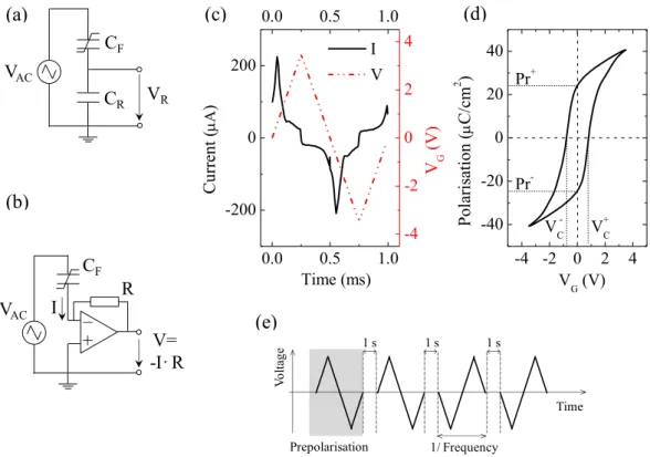
the unit cell of PZT crystal in the tetragonal ferroelectric phase.The central ion (Ti4+ or Zr4+) is displaced from the central position toward either the upper or lower oxygen ion O2–so that the centres of the net negative and positive charges are shifted relative to each other. The net electric polarisation is directed either up or down, which can represent the two logical states “0” and “1”. These two thermodynamically stable atom configurations can be described by means of a double-well potential with two equilibrium positions corresponding to the same minimum value of the free energy and separated by a potential barrier [48] (Figure 2.5(b)). At any given time the central ion of a unit cell (Ti4+ or Zr4+) is located at one of the two possible positions corresponding to one of the energy minima. In the presence of an external electric field the potential barrier is lowered so that the ion can change its position and jump into the other potential minimum. Thus, the polarisation direction is reversed. In ferroelectric materials the relationship between polarisation and electric field is represented by the hysteresis loop (Figure 2.5(c)). It can be used to extract the characteristic material parameters: the spontaneous polarisation (PS), the remanent polarisation (PR) and the coercive electric
field (EC). PS is obtained from extrapolation of the saturating linear part of the hysteresis to
zero field value, whereas PR is the actual polarisation remaining in the crystal after the electric
field has been removed. EC corresponds to the value of the external electric field with a
polarity opposite to the remanent polarisation that is required to reduce the latter to zero. PR
and EC are the decisive characteristics of ferroelectric materials for memory application and
determine the operation voltage and memory window. Table 2.1 summaries these characteristics for the most important ferroelectric thin films.
The local crystal regions with the same orientation of spontaneous polarisation are referred to as ferroelectric domains. The transition regions between domains with different polarisation directions are called domain walls and are 1 – 10 nm thick comprising only 2 – 3 unit cells [54], [55]. In ferroelectric materials a multi-domain structure is commonly formed in order to minimise the total crystal energy [56], [49]. This process is determined by the electrostatic energy associated with the depolarisation field that arises from non-compensated
Table 2.1 Key characteristics of typical ferroelectric thin films [49] – [52].
Materials PR (C/cm2) EC (kV/cm)
Pb(Zr,Ti)O3 (PZT) 25-35 50-70 300-1300
SrBi2Ta2O9 (SBT) 10-25 30-50 120-250
BaTiO3 (BTO) 3-15 30-50 300-1000
2 Fundamentals
Figure 2.6 Mechanisms of polarisation switching in ferroelectric films after [53].
polarisation charges, as well as the elastic energy associated with the mechanical constraints. The impact of mechanical stress on the formation of the domain structure is especially important in polycrystalline materials and thin films [56], [49].
Domains with different polarisations are statistically distributed in unpoled ferroelectric materials resulting in a zero net polarisation. In the presence of an external electric field, the domains reverse so that the polarisation direction of most domains coincides with that of the external field. Three regimes for the switching of the polarisation in ferroelectric films are generally distinguished [53]: nucleation of the domains with polarisations similar to the external field, forward growth of needle-like domains in the direction of the external field and sideways domain expansion (Figure 2.6). The two latter processes occur by means of domain wall motion. Nucleation commonly takes place at the electrode interface or at grain boundaries, where the formation energy is the lowest. The time needed for a nucleus to reach the critical size required for further growth is called the nucleation time, which is about 1 ns for oxide ferroelectrics [53]. The time for forward growth (tFG d v) is determined by the
film thickness (d) and the speed of sound (v). For films thinner than 1 m tFG lies in the
picosecond time range and can be neglected. The time for sideways domain growth depends on the strength of the applied electric field (E) according to 3 2
SG
t C E , where C is a constant. The rate-limiting mechanism depends on the material properties, film thickness [57], crystalline structure (monocrystalline or polycrystalline) [16], temperature [58] and lateral cell size [53]. There are two main models that describe the polarisation switching process [16]: (1) the Kolmogorov-Avrami-Ishibashi model developed by Ishibashi and Tagaki [59], [60], which treats the polarisation reversal in terms of domain wall motion, and (2) the nucleation-limited switching model proposed by Tagantsev [61], which considers the nucleation of reversed domains as the limiting switching mechanism. The first model is applicable for single crystals [62] and epitaxial films [63], whereas the second model describes the switching behaviour in polycrystalline films [61], [64]. Switching typically proceeds in the nanosecond time range (2 – 200 ns) for ferroelectric thin films [65] – [67].
2.3 Ferroelectric memories
Figure 2.7 Characteristic form of the polarisation-electric field P(E) and capacitance-electric field
C(E) curves for three material classes: (a), (b) ideal linear dielectrics, (c), (d) ferroelectrics and (e), (f) anti-ferroelectrics.
A hysteretic dependence between polarisation and electric field is a necessary but not a sufficient condition of true ferroelectricity in a material [68], [69]. Several other artefacts, such as surface polarisation, trapping-detrapping phenomena at Schottky-like electrodes [70] or leakage currents [71], can be also responsible for an experimentally detected hysteresis loop. Additional information about the true material properties can be gained by analysing the voltage dependence of the small signal capacitance. The polarisation-field and small signal capacitance-field curves characteristic for three classes of materials: linear dielectrics, ferroelectrics and antiferroelectrics, are shown in Figure 2.7. In case of linear dielectrics the electric polarisation exhibits a linear dependence from the electric field and field-independent capacitance value (Figure 2.7 (a), (b)). Polarisation hysteresis loops and butterfly-shaped capacitance-field curves are characteristic for ferroelectric materials [72], [73] (Figure 2.7 (c), (d)). The response measured during the capacitance-voltage test is associated with ionic and electronic displacements as well as with reversible domain wall motions around the local energy minima [72]. Since the domain wall concentration is highest at the coercive fields, the value of capacitance should peak at these points [72]. Antiferroelectric materials are similar to ferroelectrics in that they possess spontaneous dipoles originating from their crystal structure. The main difference is, however, that the neighbouring dipoles are aligned antiparallel to each other, resulting in a zero net polarisation. Antiferroelectrics can be field-forced to undergo a phase transition into the ferroelectric phase by applying an external electric field, when a critical field value (ECR) is achieved [74], [75]. This ferroelectric phase is, however, unstable
and transforms back into the antiferroelectric phase when the external field is removed.
P E C E P E +EC – EC C E +EC – EC P E +ECR – ECR C E +ECR – ECR (a) (b) (c) (d) (e) (f)
2 Fundamentals
loop polarisation hysteresis and double-butterfly-shaped capacitance-field curve (Figure 2.7 (e), (f)).
True ferroelectric materials should also reveal piezoelectric and pyroelectric properties in addition to a polarisation hysteresis. This follows from the classification of dielectric materials (Figure 2.8). Ferroelectrics are a special subclass of dielectric materials that belong to pyroelectrics. These are, in turn, a special subclass of piezoelectric materials. The effect of pyroelectricity is based on the temperature dependence of the spontaneous polarisation of the crystal. In a pyroelectric crystal the change in the net polarisation is proportional to the temperature change, which can be measured in a closed circuit as a current flow or in an open circuit as a voltage change across the crystal. Piezoelectricity is the property of a material to acquire an electric polarisation in response to the applied mechanical stress. This is referred as direct piezoelectric effect. The converse piezoelectric effect consists in inducing the deformation of a sample by applying an external electric field. Expansion/constriction is detected when the external electric field is parallel/antiparallel to the direction of the existing spontaneous polarisation in the sample. In ferroelectric materials the displacement versus electric field dependence has the so-called butterfly shape [77], [56], which is caused by polarisation reversal. Figure 2.9 (a) shows the correlation between the idealised polarisation and displacement loops of a ferroelectric, in which the polarisation reverses by 180° [56], [76]. In real ferroelectric materials the shape of the displacement loop is smoother (Figure 2.9 (b)) due to the distribution in the domain coercive fields and existence of non-180° domains [56]. The converse piezoelectric effect is utilised in piezoresponse force microscopy (see chapter 3.2.4) for the visualization of ferroelectric domains.
Figure 2.8 Classification of dielectric materials. Ferroelectrics are a specific subclass of dielectric materials and must possess properties of all upper classes.
Figure 2.9 Converse piezoelectric effect [76]. (a) Correlation between the idealised polarisation P(E) and displacement d(E)
loops in a ferroelectric material, in which the polarisation reverses by 180°. (b) d(E) loop shape of real ferroelectric materials. Dielectrics Piezoelectrics Pyroelectrics Ferroelectrics P E 1 2 3 4 5 6 d E 1 2 3 4 6 5 (a) (b) d E
2.3 Ferroelectric memories
Figure 2.10 Schematic illustration of the main ferroelectric degradation mechanisms after [49]: (a) fatigue, (b) retention loss and (c) imprint.
The reliability properties of ferroelectric materials are essential for their application in memory devices. Three main degradation mechanisms are commonly discussed: fatigue, retention loss and imprint. Each of them is accompanied by a specific change in the polarisation loop (Figure 2.10). The fatigue effect is a result of repetitive polarisation reversal, which causes flattening of the polarisation loop and lowering of the switchable polarisation (Figure 2.10 (a)). Several theoretical models explaining fatigue phenomenon have been developed for perovskite-type ferroelectrics [53], [78] – [82]. The degradation of the switchable polarisation is attributed to modification of the switching process during cycling, where either the domain walls get pinned by mobile charged defects [82] – [84] or the growth of domain nuclei with opposite polarity becomes inhibited [78] – [80]. Two main microscopic origins of fatigue have been proposed – oxygen vacancies [79], [85], [86], redistributing within the ferroelectric layer under electrical stress, or free charges injected from the electrodes [78], [82], [87] – [89]. Retention loss is characterised by a decrease of the polarisation with time in cells with a primary established polarisation state (Figure 2.10 (b)). The retention properties are decisive for non-volatile type memories, where the capability of information storage for at least 10 years is required [1]. The depolarisation field, internal built-in bias and charge injection are considered to be the main driving forces for polarisation loss [90] – [92]. The depolarisation field arises from incomplete compensation of the ferroelectric polarisation at the electrode interfaces. This is the case for electrodes with low free charge carrier density [91], where a depletion layer appears, or for an insulating layer with low dielectric constant, which is embedded between the electrode and the ferroelectric layer [93]. The depolarisation field is an essential issue for metal-ferroelectric-insulator-semiconductor (MFIS) stacks that can lead to retention loss. If one of the polarisation states is retained for a long time, a build-up of the internal bias can take place due to the redistribution of mobile charges within the ferroelectric layer or charge injection through the interfacial layer [16], [81]. This effect is called imprint. It is characterised by a shift of the polarisation hysteresis loop along the E-axis (Figure 2.10 (c)). The imprint effect leads to polarity
P E Cycling P E Loss of PR P E Shift of loop Loss of – PR Established state (a) (b) (c)
2 Fundamentals
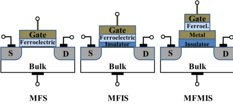
2.3.2 Types of ferroelectric memories
Ferroelectric materials can be used as an information storage media due to their ability to switch between two stable polarisation states. Progress in the fabrication of thin ferroelectric films has led to the development of two basic types of ferroelectric memories: Ferroelectric Random Access Memory (FeRAM) [42] and Ferroelectric Field Effect Transistor (FeFET) [14], [94]. These two concepts differ in the structure of the elementary memory cell and the readout approach. In the FeRAM the ferroelectric layer is integrated into the capacitor of a DRAM-like cell, resulting in a one transistor-one capacitor (1T-1C) memory cell. The FeFET-type cell consists of a single transistor (1T) with a ferroelectric layer built directly into the transistor gate-stack. The main advantages of ferroelectric memories are non-volatility, fast read/write times (under 50 ns), low operation voltages, very high endurance (greater than 10 15 write/read cycles) and low power operation [16], [1], making ferroelectric memory especially attractive for mobile applications.
The FeRAM concept is a more developed one with commercial products already available including embedded (e.g., RFID and microcontrollers) and stand-alone applications (e.g., smart cards). The ferroelectric materials most widely utilized in modern FeRAM cells are PZT [42], [95] and SBT [45], [96] films. One of the main drawbacks of this memory type is a destructive readout scheme, where the polarisation of the cell is switched in order to sense the stored memory state. A voltage pulse is applied to the capacitor during reading and a transient current response is simultaneously sensed. Depending on the initial polarisation state the ferroelectric polarisation either is reversed or remains unchanged, resulting in different value of the transient current response. Since the cell state is changed during the readout operation, it must be rewritten each time after reading. This imposes the requirement of a high endurance resistivity on the ferroelectric material used. Another important issue is the incompatibility of conventional ferroelectric compounds with standard CMOS technology. The main FeRAM integration challenges include [97], [98], [17]:
interdiffusion of ferroelectric oxides’ constituents and silicon, resulting in a performance degradation of both the ferroelectric capacitor and the transistor,
high processing temperatures of ferroelectric films, promoting interdiffusion and impacting the doping profile of the transistors,
oxidation of the interconnect metal layers due to the high pressure oxygen atmosphere used during the fabrication of the ferroelectric films,
incorporation of hydrogen into the ferroelectric films during the forming gas annealing step, impairing their ferroelectric properties,
2.3 Ferroelectric memories
In addition FeRAM, with its large cell size, can hardly compete with the conventional FG technology in the field of storage density and cost per bit. Since a FeRAM cell includes at least one transistor and one capacitor, it is difficult to scale it along with the CMOS technology roadmap. FeRAM has already faced its scaling limit at a contemporary node of 130 nm [99]. The challenge of further cell miniaturisation originates from the minimum signal level (total capacitor charge) required for sensing [100], which is directly proportional to the capacitor area.
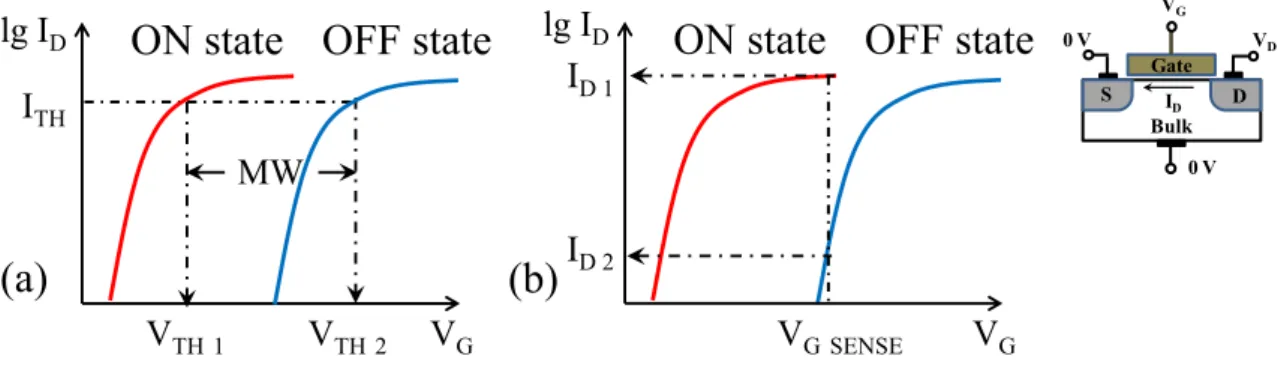
The concept of the FeFET-type memory, where the insulating layer in the gate stack of a standard field effect transistor is replaced by a ferroelectric film, was proposed in the late 1950’s [15]. Figure 2.11 schematically illustrates the structure of a FeFET memory cell and its basic operation principle using the example of an n-channel device. The conductivity of the transistor channel is modulated by the polarisation charge of the ferroelectric layer, which can be controlled by a voltage applied to the gate electrode. It should be noted that the effect of the gate voltage on the channel conductivity in FeFETs is opposite to that of charge-trapping memories (chapter 2.1.2). A positive gate voltage results in a positive polarisation charge at the ferroelectric-semiconductor interface, attracting electrons and increasing the channel conductivity. In this case the FeFET transistor is in the “ON” state with the ID-VG
characteristic shifted to lower gate voltage. An “OFF” state is induced by applying a negative gate voltage which is sufficient to reverse the ferroelectric polarisation. The conductivity of the channel decreases due to the negative polarisation charge at the ferroelectric-semiconductor interface and the ID-VG curve shifts to higher gate voltage. The readout of this
cell can be performed non-destructively by sensing the drain current without changing the polarisation of the ferroelectric layer. This relaxes the requirement for unlimited endurance stability and lowers the power consumption. Furthermore, the compactness of a one transistor (1T) cell provides better scaling potential. Since the surface charge density and not the total
Figure 2.11 Basic structure and operation principle of a FeFET-type memory cell.
p-Substrate n+ n+ Gate Ferroelectric
-+
![Figure 2.10 Schematic illustration of the main ferroelectric degradation mechanisms after [49]:](https://thumb-us.123doks.com/thumbv2/123dok_us/11109020.2998672/29.892.165.729.136.300/figure-schematic-illustration-main-ferroelectric-degradation-mechanisms.webp)

![Figure 3.5 PFM operating principle [76]. (a) Schematic representation of a measurement set-up](https://thumb-us.123doks.com/thumbv2/123dok_us/11109020.2998672/46.892.135.776.752.1016/figure-pfm-operating-principle-schematic-representation-measurement-set.webp)