University of Pennsylvania
ScholarlyCommons
Publicly Accessible Penn Dissertations
1-1-2013
High Performance Optical Transmitter Ffr Next
Generation Supercomputing and Data
Communication
Xiaotie Wu
University of Pennsylvania, [email protected]
Follow this and additional works at:
http://repository.upenn.edu/edissertations
Part of the
Communication Commons
, and the
Electrical and Electronics Commons
Recommended Citation
Wu, Xiaotie, "High Performance Optical Transmitter Ffr Next Generation Supercomputing and Data Communication" (2013).
High Performance Optical Transmitter Ffr Next Generation
Supercomputing and Data Communication
Abstract
High speed optical interconnects consuming low power at affordable prices are always a major area of research focus. For the backbone network infrastructure, the need for more bandwidth driven by streaming video and other data intensive applications such as cloud computing has been steadily pushing the link speed to the 40Gb/sand 100Gb/sdomain. However, high power consumption, low link density and high cost seriously prevent traditional optical transceiver from being the next generation of optical link technology. For short reach communications, such as interconnects in supercomputers, the issues related to the existing electrical links become a major bottleneck for the next generation of High Performance Computing (HPC). Both applications are seeking for an innovative solution of optical links to tackle those current issues.
In order to target the next generation of supercomputers and data communication, we propose to develop a high performance optical transmitter by utilizing CISCO Systems®'s proprietary CMOS photonic technology. The research seeks to achieve the following outcomes:
1. Reduction of power consumption due to optical interconnects to less than 5pJ/bitwithout the need for Ring Resonators or DWDM and less than 300fJ/bitfor short distance data bus applications.
2. Enable the increase in performance (computing speed) from Peta-Flop to Exa-Flops without the proportional increase in cost or power consumption that would be prohibitive to next generation system architectures by means of increasing the maximum data transmission rate over a single fiber.
3. Explore advanced modulation schemes such as PAM-16 (Pulse-Amplitude-Modulation with 16 levels) to increase the spectrum efficiency while keeping the same or less power figure.
This research will focus on the improvement of both the electrical IC and optical IC for the optical transmitter. An accurate circuit model of the optical device is created to speed up the performance
optimization and enable co-simulation of electrical driver. Circuit architectures are chosen to minimize the power consumption without sacrificing the speed and noise immunity.
As a result, a silicon photonic based optical transmitter employing 1V supply, featuring 20Gb/sdata rate is fabricated. The system consists of an electrical driver in 40nmCMOS and an optical MZI modulator with an RF length of less than 0.5mmin 0.13&mu mSOI CMOS. Two modulation schemes are successfully
demonstrated: On-Off Keying (OOK) and Pulse-Amplitude-Modulation-N (PAM-N N=4, 16). Both versions demonstrate signal integrity, interface density, and scalability that fit into the next generation data communication and exa-scale computing. Modulation power at 20Gb/sdata rate for OOK and PAM-16 of
4pJ/bitand 0.25pJ/bitare achieved for the first time of an MZI type optical modulator, respectively.
Degree Type Dissertation
Degree Name
Graduate Group
Electrical & Systems Engineering
First Advisor Jan Van der Spiegel
Subject Categories
HIGH PERFORMANCE OPTICAL TRANSMITTER FOR NEXT GENERATION SUPERCOMPUTING AND DATA COMMUNICATION
Xiaotie Wu
A DISSERTATION
in
Electrical and Systems Engineering
Presented to the Faculties of the University of Pennsylvania
in
Partial Fulfillment of the Requirements for the
Degree of Doctor of Philosophy
2013
Supervisor of Dissertation
Jan Van der Spiegel, Professor, Electrical and Systems Engineering
Graduate Group Chairperson
Saswati Sarkar, Professor, Electrical and Systems Engineering
Dissertation Committee
Nader Engheta, H. Nedwill Ramsey Professor, UPENN
Kenneth R. Laker, Professor, UPENN
Dale Nelson, Adjunct Professor, UPENN
HIGH PERFORMANCE OPTICAL TRANSMITTER FOR NEXT GENERATION
SUPERCOMPUTING AND DATA COMMUNICATION
c
COPYRIGHT
2013
Xiaotie Wu
This work is licensed under the
Creative Commons Attribution
NonCommercial-ShareAlike 3.0
License
To view a copy of this license, visit
ACKNOWLEDGEMENT
Although this work bears my name as the only author, it would not have been possible
without the support and help of many people to whom I would like to express my greatest
gratitude.
First, I would like to thank my advisor, Professor Jan Van der Spiegel, who offered me this
fantastic opportunity to do research in his group and patiently guided me through my entire
Ph.D. study. From him, I not only learned how to write a good paper and give an impressive
presentation, but also learned how to become a competent researcher. I would also like to
thank my committee members, Professor Kenneth R. Laker, Professor Nader Engheta and
Professor Dale Nelson, for the intriguing class they taught and knowledgeable answers to
my research questions.
I am indebted to the companies, Lightwire and CISCO Systems, who sponsored this
re-search program both financially and technically for the past two years. In 2012 Lightwire
was acquired by CISCO, who continued to support this work by granting me access to
their latest silicon photonic technology, providing me the EDA tools, chip fabrication and
lab equipments.
I would like to give my very special thanks to Kal Shastri, founder and CTO of Lightwire,
for bringing me onto the team at Lightwire and introducing me to the exciting field of silicon
photonics and showing me so many amazing technological applications.
I am also grateful to the management team, Kaushik Patel, Bipin Dama, and Sanjay Sunder
at CISCO, for the trust in assigning me with projects, patient mentoring, and
encourage-ments despite results. I don’t believe I will ever be able to find another work environment
with such an amazing group of individuals who are so capable, creative, and supportive of
my personal development on so many different levels - professionally and intellectually.
Craig, Dale, Gregg, Joe, Mark, Peter, Pratix, Rajesh, Som, Terry, Will and Yifan. From
them, I’ve been able to gain a new and deeper understanding in silicon photonics as well
as in IC designs. Without them working day and night, in supporting of my designs, I might
have pushed out the tape-out date for decades.
I would also like to especially thank the Post Doc Milin Zhang and former Ph.D. student
Chengjie Zuo at UPENN, for their kindly help in the design, simulation and characterization
of the wire-grid polarization senor and low power MEMS oscillator.
Last but not least, I would like to thank my wife and parents, for their constant support,
ABSTRACT
HIGH PERFORMANCE OPTICAL TRANSMITTER FOR NEXT GENERATION
SUPERCOMPUTING AND DATA COMMUNICATION
Xiaotie Wu
Jan Van der Spiegel
High speed optical interconnects consuming low power at affordable prices are always a
major area of research focus. For the backbone network infrastructure, the need for more
bandwidth driven by streaming video and other data intensive applications such as cloud
computing has been steadily pushing the link speed to the 40Gb/sand 100Gb/sdomain.
However, high power consumption, low link density and high cost seriously prevent
tra-ditional optical transceiver from being the next generation of optical link technology. For
short reach communications, such as interconnects in supercomputers, the issues related
to the existing electrical links become a major bottleneck for the next generation of High
Performance Computing (HPC). Both applications are seeking for an innovative solution of
optical links to tackle those current issues.
In order to target the next generation of supercomputers and data communication, we
pro-pose to develop a high performance optical transmitter by utilizing CISCOR’s proprietary
CMOS photonic technology. The research seeks to achieve the following outcomes:
1. Reduction of power consumption due to optical interconnects to less than 5pJ/bit
without the need for Ring Resonators or DWDM and less than 300f J/bit for short
distance data bus applications.
2. Enable the increase in performance (computing speed) from Peta-Flop to Exa-Flops
without the proportional increase in cost or power consumption that would be
data transmission rate over a single fiber.
3. Explore advanced modulation schemes such as PAM-16 (Pulse-Amplitude-Modulation
with 16 levels) to increase the spectrum efficiency while keeping the same or less
power figure.
This research will focus on the improvement of both the electrical IC and optical IC for the
optical transmitter. An accurate circuit model of the optical device is created to speed up the
performance optimization and enable co-simulation of electrical driver. Circuit architectures
are chosen to minimize the power consumption without sacrificing the speed and noise
immunity.
As a result, a silicon photonic based optical transmitter employing 1V supply, featuring
20Gb/sdata rate is fabricated. The system consists of an electrical driver in 40nmCMOS
and an optical MZI modulator with an RF length of less than 0.5mmin 0.13µmSOI CMOS.
Two modulation schemes are successfully demonstrated: On-Off Keying (OOK) and
Pulse-Amplitude-Modulation-N (PAM-N N=4, 16). Both versions demonstrate signal integrity,
interface density, and scalability that fit into the next generation data communication and
exa-scale computing. Modulation power at 20Gb/s data rate for OOK and PAM-16 of
4pJ/bit and 0.25pJ/bit are achieved for the first time of an MZI type optical modulator,
TABLE OF CONTENTS
ACKNOWLEDGEMENT . . . iv
ABSTRACT . . . vi
LIST OF TABLES . . . xi
LIST OF ILLUSTRATIONS . . . xviii
CHAPTER 1 : Introduction . . . 1
CHAPTER 2 : High Speed Interconnect Overview . . . 8
2.1 Interconnect at a Glance . . . 8
2.1.1 Wireless Interconnect . . . 9
2.1.2 Electrical Wireline Interconnect . . . 10
2.1.3 Optical Interconnect . . . 16
2.2 Optical Communication Overview . . . 17
2.2.1 System Architecture . . . 19
2.2.2 Modulation Format and Spectral Efficiency . . . 21
2.3 Light Fundamental . . . 23
2.3.1 Light Property . . . 23
2.3.2 Material’s Physical Effects . . . 28
2.4 Optical Modulator Classification . . . 32
2.4.1 Direct Modulation . . . 33
2.4.2 Electroabsorption Modulator . . . 34
2.4.3 Phase Modulator . . . 34
2.4.4 Mach-Zehnder Interferometer(MZI) Modulator . . . 35
2.5 Optical Modulator Characteristics . . . 38
2.6 Silicon Photonics Based Optical Modulator . . . 43
2.6.1 Electrical Structure of Silicon Photonic Modulator . . . 44
2.6.2 Optical Structure of Silicon Photonic Modulator . . . 47
2.7 Summary . . . 49
CHAPTER 3 : SISCAP MZM Model . . . 51
3.1 SISCAP MZM Overview . . . 52
3.1.1 Structure Detail . . . 52
3.1.2 SISCAP MZM Operation Principle . . . 55
3.1.3 Driver and Driving Scheme . . . 57
3.1.4 Performance . . . 59
3.2 SISCAP Characteristics . . . 60
3.2.1 Physical Effects in SISCAP . . . 60
3.2.2 Carrier Concentration . . . 62
3.2.3 Electrical Parameter . . . 65
3.2.4 Simulation of SISCAP . . . 70
3.3 Circuit Model of Optical IC . . . 73
3.3.1 Model Hierarchy . . . 76
3.3.2 Model of MZI . . . 78
3.3.3 Model of SISCAP . . . 81
3.3.4 Model of Bond Wire . . . 85
3.3.5 Model of Routing Parasitic . . . 86
3.3.6 Simulation and Experiment Result . . . 86
3.4 Summary . . . 89
CHAPTER 4 : Optical Transmitter Performance Optimization . . . 90
4.1 System Architecture . . . 90
4.2.1 Bandwidth Enhancement . . . 93
4.2.2 Power Reduction . . . 99
4.2.3 Polarization . . . 109
4.2.4 Integrated Polarization Detection Imager . . . 109
4.3 Electrical Driver Performance Optimization . . . 122
4.3.1 System Level . . . 122
4.3.2 VCO and Tunable MEMS Based Oscillator . . . 127
4.3.3 Clock and Data Recovery . . . 138
4.4 Measurement Result . . . 144
4.4.1 Test Setup . . . 145
4.4.2 Characterization Result . . . 148
4.5 Summary . . . 152
CHAPTER 5 : Conclusion and Future Works . . . 154
5.1 Summary . . . 154
5.2 Future Work . . . 156
LIST OF TABLES
TABLE 2.1 : Inerstion Loss (IL) comparison of different channels. . . 14
TABLE 2.2 : Recent development of PDM systems. . . 22
TABLE 2.3 : Comparison of different link technologies with silicon photonic mod-ulator . . . 49
TABLE 3.1 : Silicon photonic modulator tuning method tradeoffs . . . 65
TABLE 4.1 : Encoding table for different PAM-16 implementations. . . 104
TABLE 4.2 : Comparison of focal plane polarization image sensor. . . 121
TABLE 4.3 : Measured power consumption at different power supply. . . 136
TABLE 4.4 : Comparison of performances in literature. . . 137
LIST OF ILLUSTRATIONS
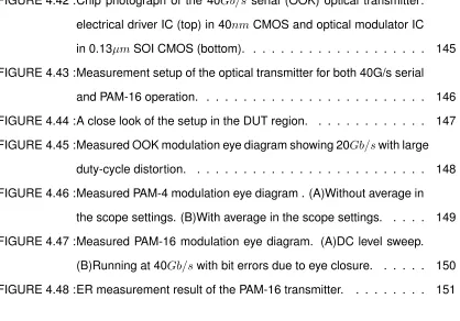
FIGURE 1.1 : Global IP traffic forcast.(Source: Cisco VNI, 2012) . . . 1
FIGURE 2.1 : Moore’s Law of IC (data is compiled from various data sheets and
web sources): (A)CPU Total Transistor Count. (B)CPU Frequency.
(C)GPU Total Transistor Count. (D)FPGA Total Transistor Count. 12
FIGURE 2.2 : IEEE802.3 100Gb/sbackplane insertion loss (Data is from IEEE
website). . . 13
FIGURE 2.3 : Causes of copper channel loss: (A) Skin effect. (B) Surface
rough-ness. (C) Dielectric loss . . . 14
FIGURE 2.4 : System diagram of a DWDM optical link. . . 19
FIGURE 2.5 : Constellation diagrams of different modulation formats in optical
communications. . . 21
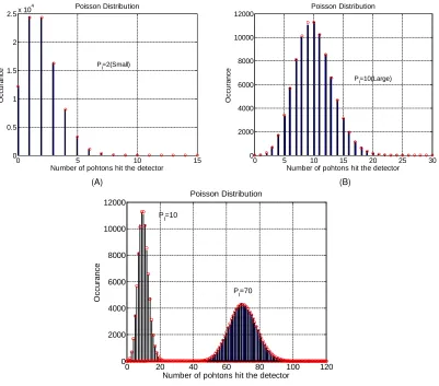
FIGURE 2.6 : Simulation result of photon shot noise.PIis the number of
interac-tion photons with the photo detector. (A)Distribuinterac-tion when number
of photons that interact with detector is small. (B)Distribution when
number of photons that interact with detector is large. (C)Distribution
with different number of photons that interact with detector. . . . 27
FIGURE 2.7 : Optical Modulator Classification. . . 32
FIGURE 2.8 : (A)VCSEL cross section. (B)VCSEL output power v.s. bias
volt-age. (C)VCSEL driving diagram. . . 33
FIGURE 2.9 : Mach-Zehnder interferometer (MZI) modulator working diagram. 35
FIGURE 2.10 :Fabry-Perot modulator (A)Modulator diagram (B)Maximum output
condition (C)Transmittance curve . . . 37
FIGURE 2.11 :(A) Ring resonator modulator diagram. (B)Electric field simulation
of ring modulator. . . 38
FIGURE 2.13 :Extinction ratio and power efficiency comparison. . . 40
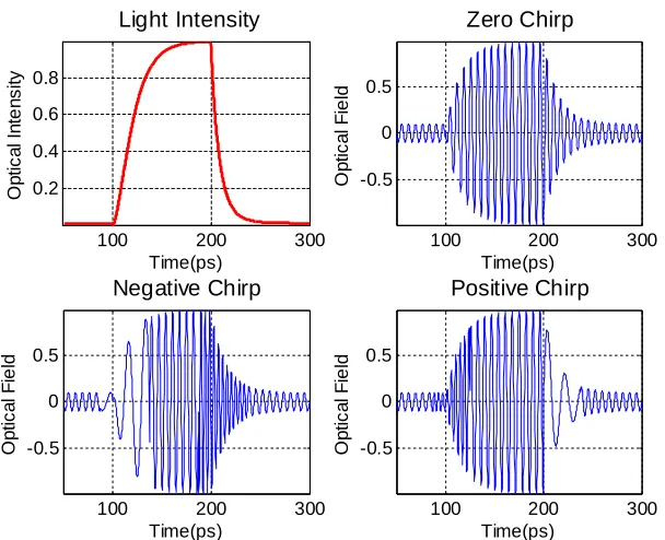
FIGURE 2.14 :Diagram of light pulse and different types of chirp. . . 42
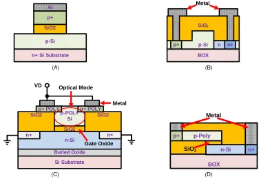
FIGURE 2.15 :(A)Cross section of P-i-N silicon modulator. (B)Cross section of
PN junction silicon modulator. (C)Cross section of MOS capacitor
silicon modulator. (D)Cross section of SISCAP silicon modulator. 45
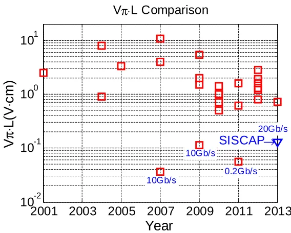
FIGURE 2.16 :Vπ ·Lcomparison chart of different modulator technologies (data
is compiled from various research publications). . . 46
FIGURE 2.17 :(A)MZM based on SISCAP (Courtesy of CISCO Systems). (B)Ring
resonator based on forward biased lateral P-i-N diode. . . 47
FIGURE 3.1 : (A)Diagram of SISCAP based MZM. (B)Cross section of SISCAP
structure (Courtesy of CISCO). . . 53
FIGURE 3.2 : SISCAP high frequency capacitance versus applied voltage. . . . 54
FIGURE 3.3 : Output optical power transfer curve in SISCAP MZM. . . 56
FIGURE 3.4 : (A)Differential driving of SISCAP MZM. (B)Common-poly driving
of SISCAP MZM. (C)Asymmetric poly driving of SISCAP MZM. . 58
FIGURE 3.5 : SISCAP electrical structure. . . 62
FIGURE 3.6 : SISCAP band diagram at different bias conditions (not drawn to
scale). (A)V a=VF B. (B)V a > VF B. (C)V a < VF B . . . 63
FIGURE 3.7 : SISCAP capacitance. (A)At low frequency. (B)At high frequency. 66
FIGURE 3.8 : SISCAP capacitance break down. (A)In accumulation region. (B)In
depletion region. . . 67
FIGURE 3.9 : Simulated SISCAP C-V curve with different gate oxide thickness. 68
FIGURE 3.10 :Simulated SISCAP C-V curve at different doping levels. . . 69
FIGURE 3.11 :FDTD electrical domain simulation results in SISCAP. (A)Electric
field (V/cm). (B)Hole concentration (cm−1).(C)Electron
FIGURE 3.12 :FDTD simulation result of the optical mode (electric field) in
SIS-CAP and MOSSIS-CAP. (A)SISSIS-CAP with λ = 1310nm. (B)SISCAP
withλ= 1550nm. (C)MOSCAP withλ= 1310nm . . . 74
FIGURE 3.13 :FDTD simulation result of the phase shift in SISCAP. . . 75
FIGURE 3.14 :Top level circuit model diagram of the SISCAP based MZI. . . 76
FIGURE 3.15 :Model hierarchy created in this research. . . 77
FIGURE 3.16 :Optical transfer function in the MZI structure. . . 78
FIGURE 3.17 :Electrical model of SISCAP created in this research. . . 82
FIGURE 3.18 :Measured SISCAP capacitance vs voltage and the comparison with curve fitting result. . . 82
FIGURE 3.19 :Measurement result and curve fitting comparison. (A)SISCAP at-tenuation vs voltage. (B)SISCAP phase shift vs voltage. . . 84
FIGURE 3.20 :Transmitter connection diagram. . . 85
FIGURE 3.21 :Wire bond model. . . 86
FIGURE 3.22 :Simulation result of the bond wire model. (A)Self inductance and mutual inductance. (B) Skin depth and resistance for 800µmlong bond wire. (C) Mutual capacitance for different bond wire distance ‘D’. . . 87
FIGURE 3.23 :Simulated eye diagram (on the top) and measured optical eye dia-gram (on the bottom) at different data rate. (A)10Gb/s. (B)28Gb/s. . . . 88
FIGURE 4.1 : System architecture of the proposed optical transmitter. . . 90
FIGURE 4.3 : Simulated optical eye diagram at 40Gb/swith 480µmSISCAP RF
section. . . 96
FIGURE 4.4 : 1-tap FFE implementation in SISCAP MZM. . . 97
FIGURE 4.5 : ∆φchange in the MZM. (A)Without traveling wave matching. (B)With
traveling wave matching. . . 97
FIGURE 4.6 : Measured OOK modulation eye diagram from the test chip. (A)32Gb/s
PRBS7 electrical input. (B)32Gb/sPRBS7 optical output. (C)40Gb/s
PRBS31 electrical input. (D)40Gb/sPRBS31 optical output. . . . 98
FIGURE 4.7 : Simplified MZI driver diagram for power consumption analysis. . 100
FIGURE 4.8 : Different PAM schemes. (A)PAM-2(OOK). (B)PAM-4. (C)PAM-16. 102
FIGURE 4.9 : Implementation methods of PAM-16 with segmented SISCAP MZM:
PAM-2 or OOK (top), binary code weighted PAM-16 (middle) and
thermometer code weighted PAM-16 (bottom). . . 103
FIGURE 4.10 :(A)Binary/thermometer code weighted PAM-N (N=8 in this plot).
(B)Enhanced binary code weighted PAM-N (N=8 in this plot). . . 105
FIGURE 4.11 :MZM structure implementing the enhanced binary code weighted
PAM-16 scheme. . . 105
FIGURE 4.12 :PAM-N (N=4 in this plot) level position optimization. (A)Before
op-timization: the 4 levels are unequally spaced. (B)Using 3 SISCAP
segments with random lengths to generate 8 levels. (C)After
op-timization: 4 levels with equal space are pick from (B) to get the
final PAM-4. . . 106
FIGURE 4.13 :Output intensity distribution in PAM-N. (A)With equally spaced
out-put levels. (B)With optimum outout-put level spacing. . . 107
FIGURE 4.14 :Simulated PAM-16 optical eye diagram with PRBS31 pattern. (A)Data
rate is 40Gb/s with symbol rate = 10GBaud/s. (B)Data rate is
112Gb/swith symbol rate = 28GBaud/s. . . 108
FIGURE 4.16 :FDTD simulation model (right) and electrical field (left) of metal
wire grid polarization filter. . . 112
FIGURE 4.17 :Simulation results of the extinction ratio for a single layer wire-grid
made of the first metal layer (M1), while (A) wire-grid periodΛis
increasing from 100nmto 180nmwith a fixed wire-grid duty cycle
of 50%; (B) the duty cycle of the wire-grid is increasing from 40%
to 80%with a fixedΛ = 200nm. The extinction ratio is evaluated
for different incident wavelength varying from 450nmto 650nm. . 113
FIGURE 4.18 :A comparison of the extinction ratio performance while different
metal layer is selected for a single layer wire-grid implementation. 114
FIGURE 4.19 :Simulation result of metal wire grid polarizer at communication
wave length: ER (top), transmission efficiency T⊥ (middle) and
reflection efficiencyR⊥(bottom). . . 115
FIGURE 4.20 :(A) Circuit diagram of the overall system. The32×32active pixel
sensor (APS) array is divided into2×2blocks. Within each block,
three wire-grid polarizer filters are implemented on top of the
pho-todiode region. The architecture of the pixel and current conveyor
is illustrated on the right. (B)Microphotography of the the
polariza-tion image sensor. (C)Layout of the45◦ wire grid with an effective
period of about 250nm. . . 117
FIGURE 4.21 :(A)Metal stack of the 65nm CMOS process. (B)Wire grid cross
section. (C)Pixel mosaic structure. . . 118
FIGURE 4.22 :Test setup of the polarization image sensor. . . 118
FIGURE 4.23 :Measurement result. (A)Transmission efficiency. (B)Phase error
of pixels covered by wire-grid with a different layout orientations
of0◦,45◦ and 90◦. The degree value on the x-axis is the rotation
angle of the polarizer on the path of the incident. . . 120
FIGURE 4.25 :Top level circuit diagram of the transmitter. . . 123
FIGURE 4.26 :DLL based Frequency doubler. . . 125
FIGURE 4.27 :Simulation of 40nmprocess inverter chain at 1.0V supply. (A)Testbench. (B)Waveform for SS process, -40◦C. . . 126
FIGURE 4.28 :(A) SEM photo of the AlN CMR and the MBVD circuit model of the resonator, (B) Measured AlN CMR admittance curve. . . 130
FIGURE 4.29 :Schematic of the tunable Pierce oscillator working in sub-threshold region. . . 131
FIGURE 4.30 :(A) Simulated transient waveform of the oscillator. (B) Simulated frequency tuning range. . . 133
FIGURE 4.31 :Photo of the oscillator system (Left: Electrical IC, Right: MEMS resonator). . . 134
FIGURE 4.32 :Characterization result with 3 different resonators: 204M Hz(Top), 517M Hz(Middle) and 850M Hz(Bottom). (A)Measured output fre-quency. (B)Measured frequency variation. . . 135
FIGURE 4.33 :Measured phase noise of the 204MHz oscillator. . . 137
FIGURE 4.34 :Master-slave CDR top level diagram. . . 138
FIGURE 4.35 :Half rate bang-bang CDR timing diagram. . . 139
FIGURE 4.36 :Phase detector design: using CML logic (top) and using CMOS logic (bottom). . . 140
FIGURE 4.37 :Dynamic D flip-flop built with transmission gate inverter. . . 141
FIGURE 4.38 :Circuit diagram of the phase interpolator. . . 142
FIGURE 4.39 :Phase interpolator’s output with different input waveform. Bold red curve is inputIP. Bold green curve is inputQP. Thin blue curve is the output signal after interpolation. . . 143
FIGURE 4.40 :Clock buffer and duty cycle correction. . . 143
FIGURE 4.42 :Chip photograph of the 40Gb/s serial (OOK) optical transmitter:
electrical driver IC (top) in 40nmCMOS and optical modulator IC
in 0.13µmSOI CMOS (bottom). . . 145
FIGURE 4.43 :Measurement setup of the optical transmitter for both 40G/s serial
and PAM-16 operation. . . 146
FIGURE 4.44 :A close look of the setup in the DUT region. . . 147
FIGURE 4.45 :Measured OOK modulation eye diagram showing 20Gb/swith large
duty-cycle distortion. . . 148
FIGURE 4.46 :Measured PAM-4 modulation eye diagram . (A)Without average in
the scope settings. (B)With average in the scope settings. . . 149
FIGURE 4.47 :Measured PAM-16 modulation eye diagram. (A)DC level sweep.
(B)Running at 40Gb/swith bit errors due to eye closure. . . 150
CHAPTER 1 : Introduction
Wireline interconnects, as a medium of conveying information, exist in every scale of
peo-ple’s daily lives. On the macro level, the inter-continental IP network has greatly influenced
the way of how people communicate, work and entertain. On the micro level, the
nanome-ter wide metal wire inside a modern integrated circuits is an essential element responsible
for transmitting and receiving signals among transistors.
2010 2011 2012 2013 2014 2015 2016 Business 47,160 59,304 91,356 112,500 134,724 157,560 91,356 Consumer 194,652 309,504 446,928 566,376 715,824 913,236 1,165,82
0 200,000 400,000 600,000 800,000 1,000,000 1,200,000 1,400,000
Traf
fi
c(Pet
aBytes)
Annual Global IP Traffic Forcast
Figure 1.1: Global IP traffic forcast.(Source: Cisco VNI, 2012)
Despite of the economy contracting since 2008, the network traffic as shown in Figure 1.1,
driven by streaming video and other data intensive applications such as cloud computing
has been steadily increasing and is expected to reach 110.3 exa-bytes per month or nearly
1.3 zetta-byte (1.3×10²¹ Bytes) per year by the end of 2016 [1], which is equivalent to a compound annual growth rate of 29%. The demand mostly comes from consumer traffic
which will, in 2016, account for more than 90%of all internet traffic because of the widely
Thirst for bandwidth also exists in the supercomputers and data centers driven by
cus-tomers from financial services, technical companies and military. One major barrier to take
supercomputing to the next level are limitations on data transmission rates between CPUs
and memory, and the connections that switch between CPU nodes for parallel
process-ing. Supercomputer’s tremendous speed is achieved through “parallel processing” which
allows thousands of CPUs to work in concert through a series of switches. The current
design of supercomputers requires significant cabling to tie together inter-node links using
materials that are inefficient, resulting in high energy requirements and high costs for the
operation. Statistics shows that almost 15%∼ 23% of energy is consumed by the
inter-connects [2]. Existing supercomputer such as Roadrunner [3] has a significant appetite
for power, consuming roughly three megawatts of power, or about the power required by a
large suburban shopping center. The power needs for a Japanese supercomputer
devel-oped by Fujitsu Labs is in the neighborhood of 13 megawatts [4], which would likely require
its own power station.
Similarly, seeking for higher speed is the ultimate goal for the semiconductor industry
be-cause of the increasingly demand on computational power. Benefit from the semiconductor
processing scaling down, the total transistor count as well as the overall chip performance
of today’s computer processors follows pretty well Moore’s law. However, this trend does
not apply to the maximum clock frequency a processor can operate mainly because of
the on-chip interconnect delays introduced by the parasitic R and C. It is more likely that
the chip speed will be limited by the wire delay instead of the transistor’s transit frequency
fT which is generally higher for finer process nodes. This speed gap is one of the major
issues for further improving the performance of processors.
Traditionally, the medium for long distance data communication is dominated by optical
fiber because of its high speed, low loss, and excellent signal integrity. However, high
power consumption, low link density and high cost seriously prevent traditional optical
For short reach applications, although copper is the most cost-effective choice for
intercon-nect, the issues related to the existing electrical links such as high power, low bandwidth
and cross talk become major bottlenecks for the next generation of High Performance
Computing (HPC).
As the communication bandwidth requirement increases at its current exponential rate,
copper and traditional optoelectronics interconnects currently provide these connections
are hitting a wall in terms of power consumption, signal integrity and cost limitations at
high speeds. Both applications are seeking for an innovative solution of link technology to
tackle those current issues.
Compared to other emerging or novel interconnect technologies such wireless, nanowire,
Single-Walled Carbon Nanotube (SWCNT) and superconductor, optical is still the best
candidate with a foreseeable future to meet both the performance and commercialization
standard. There is already a tendency of replacing copper wires with optical links in all
system levels even for the IC’s on-chip interconnection [5].
Among all building blocks, finding better method for controlling light is the key element to
build the optical link which has drawn extensive research attention for the past 60 years
since the invention of the laser [6]. In order to address the current issues related to the
optical and electrical links and target the next generation of supercomputers and data
communication, we propose to develop a high performance optical transmitter by utilizing
CISCOR’s proprietary CMOS photonic technology. The research would seek to achieve
the following outcomes:
1. Reduction of power consumption due to optical interconnects to less than 5pJ/bit
without the need for ring resonator modulators and less than 300f J/bit for short
distance data bus applications.
2. Enable the increase in performance (computing speed) from Peta-Flop to Exa-Flops
pro-hibitive to next generation system architectures by means of increasing the maximum
data transmission rate over a single fiber. The goal is to achieve 40Gb/stransmission
data rate using single fiber and single wavelength without using Dense Wavelength
Division Multiplexing (DWDM).
3. Explore the advanced modulation scheme such as PAM-16 to increase the spectrum
efficiency while keeping the same or less power figure.
However, realizing these targets is not trivial. It requires significant research and
develop-ment efforts with heavily investdevelop-ment on equipdevelop-ment, software and human resource. A group
of people at Lightwire (currently CISCO) have been actively involved in this development
process for more than 10 years. This research, as a part of this large project, will focus
on the improvement of both electrical IC and optical IC for the optical transmitter based on
their existing work. An accurate circuit model of the optical device is created to speed up
the performance optimization and enable co-simulation of electrical driver. Circuit
architec-tures and sub blocks are chosen to minimized the power consumption without sacrificing
the speed and noise immunity.
Major challenges of this research are:
1. How to precisely model the behaviors of the electrical IC and optical IC to optimize
their performance.
2. How to push the speed limit of current CMOS technology higher to the 40Gb/srange.
3. How to keep the power figure low with the presence of various leakage sources and
routing parasitics.
4. How to deal with non-ideal factors such as supply noise and signal interference.
None of them are trivial for circuits running above 10GHz. Efforts have been made to
As a result, a silicon photonic based optical transmitter employing 1V supply, featuring
20Gb/sdata rate is fabricated. The system consists of an electrical driver in 40nmCMOS
and an optical MZI (Mach-Zehnder Interferometer) modulator with an RF length of less than
0.5mmin 0.13µm SOI CMOS. Two modulation schemes are successfully demonstrated:
OOK (On-Off Keying) and Pulse-Amplitude-Modulation-N (PAM-N N=4, 16). Both versions
demonstrate signal integrity, interface density, and scalability that fit into the next generation
data communication and exa-scale computing. Modulation power at 20Gb/sdata rate for
OOK and PAM-16 of 4pJ/bitand 0.25pJ/bitare achieved for the first time of an MZI type
optical modulator, respectively.
The contribution of this thesis is summarized as follows:
1. Enhance the existing model of the optical device from Lightwire by adding more
accu-rate parasitic R, L, C information such as bond wire’s mutual inductance, skin effect,
and S-parameter model of the routing. Besides the parasitic components, the model
also incorporates the voltage and temperature dependency. Geometry dependent
information is also added which means the final model is almost fully parameterized.
Thus, the user can simply set the size, doping, voltage, and etc to get the device’s
performance simulated.
2. MZI(Mach-Zehnder Interferometer) models for advanced modulation scheme have
been created including 5 different versions: 40Gb/sserial, PAM-16 binary weighted,
PAM-16 thermometer weighted, PAM-16 enhanced binary weighted, and PAM-16
enhanced thermometer weighted. Other designers can use these models to optimize
the MZI length and determine the best scheme to be implemented.
3. Electrical circuits supporting the operation of the MZI have been developed which
are: 1) Phase picking CDR(clock and data recovery); 2) Resistive termination with
adjustable range and automatic calibration circuit to compensate for PVT variation;
temper-ature sensor which are migrated from different process based on existing Lightwire’s
designs.
4. Matlab model of CDR is created and simulated to evaluating the jitter tolerance
per-formance. The jitter budget analysis is then carried out to help selecting the structure
of the CDR.
5. A MEMS(Micro-Electro-Mechanical Systems) based tunable oscillator is designed to
explore the possibility of further reducing the power consumption.
6. Explore the possibility of using the on-chip metal wire grid to detect the polarization
status of light. An image sensor integrated with focal plane2×2wire-grid polarizer
filter mosaic targeted at visible spectrum is designed.
The thesis comprises 5 chapters. Chapter 2 starts with an general overview of the high
speed interconnects. The advantages and issues with existing technologies are briefly
compared. The remaining sections will focus on the optical interconnect, covering the
both the system level structure and key building blocks. The fundamental properties of
light and its interactions with materials such as electro-absorptive effect, electro-optical
effect and free carrier effect, are described first. The classification and key parameters to
characterize the optical modulator is then discussed in detail. Finally, the optical modulator
based on silicon photonic technology is introduced. Various modulator structures, such
as ring resonator, PN junction based MZI, PIN based MZI , and SISCAP based MZI are
presented in detail. Finally, the chapter will conclude with the performance comparison of
different modulator architectures.
Chapter 3 first introduces basic the structure and key parameters of the SISCAP structure.
A simplified analytical model is then created and discussed. More accurate numerical
simulation is performed and result is given. Based on the model and lab characterization,
a circuit model is constructed which enable the co-simulation of SISCAP with the electrical
Chapter 4 is devoted to the performance optimization of the SISCAP based MZI
transmit-ter. The research focuses on the improvement both the electrical IC and optical IC. The
techniques to reduce the power as well as increase the operating speed are discussed in
detail from the system level down to each building blocks. Simulation result and
measure-ment data are then presented and discussed.
An overall summary of this dissertation is provided in Chapter 5. Suggestions for future
CHAPTER 2 : High Speed Interconnect Overview
This chapter first introduces the background of different interconnect technologies with
more emphasis on the optical links. Among all the building blocks in an optical
communi-cation link, the transmitter especially the optical modulator serves a more important role.
The rest of this chapter concentrates on the optical transmitter technology, starting by
in-troducing the fundamental properties of light. Then, the interaction of materials with light
will be described in detail which serves as the basis of most of the optical modulators.
Nex-t, a classification of optical modulators will be given followed by the major parameters to
characterize the performance of the modulator. Last but not least, the silicon based optical
modulators will be presented. The key parameters of different modulators are summarized
in the end of this chapter.
2.1. Interconnect at a Glance
Communication, coming from the Latin word “communis” which means to share, is the
activity of exchanging information, messages, or thoughts and exists in every aspects of
our society [7]. Interconnect, as the medium of communication, enables the convey of
information by various means such as sound, visuals, or optics/electric signals etc. The
developments of interconnect technologies make possible the communication from billions
of miles between the the earth and the satellite “Voyager1” [8] down to tens of nanometers
between two transistors in the latest generation of computer processor [9].
Theoretically, any detectable changes can be used to carry information. Thus,
intercon-nection can be realized in various approaches. It could be the mechanical vibration of air
stimulated by human’s speech where the combinations of pitches and intensity represent
different meanings. It could be the beacon out of a lighthouse where colors, intensity and
on/off interval provide important information, such as weather conditions, reef locations
and status of an airport. It could be the electrical signals going either wirelessly in the air
full of data travelling at 60mph on the highway which may have more bandwidth than most
of our home networks. It could also be the quantum status of an atom travelling faster than
light in the teleportation [10] predicted by Albert Einstein’s theory of special relativity [11].
Among all the realizations of interconnects, three of them are most widely adopted by
modern information systems for different applications:
1. Wireless signals via the air
2. Electrical signals carried by metal wire
3. Optical signals through fiber
The choice of which technique to implement is determined by the systems’ unique
char-acteristics which lead to trade-offs among speed, distance, power, cost and deployment
difficulty, just to name a few.
2.1.1. Wireless Interconnect
Wireless interconnect is undoubtedly the first choice for applications where mobility is
im-portant such as in the cell phone market, or when it is impossible to establish a wired
connection such as in communications between the earth and satellite. Beside the
con-venience that user device can move easily within the signal range, wireless also has the
advantages of easy and inexpensive to deploy since there is no need for cabling
infras-tructures and devices. In addition, it can easily support hundreds of users simultaneously
through either broadcasting or multiplexing.
However, wireless has its own disadvantages such as relatively lower bandwidth, limited
working ranges affected by environment condition, and less security. Due to attenuation
and interference, the wireless link can not support very high data rate. Even the latest
802.11ac WiFi standard [12] can only reach 867M b/swithin tens of meter using a single
antenna. Going to higher carrier frequencies such as 60GHz can provide more bandwidth
network from GSM to 3G or 4G LTE, the global mobile phone sales reached 472 million
units in the fourth quarter of 2012 [13],44%of which are smart phones with data network
feature. In order to support the explosive network traffic, the backbone system in the base
station has to use electrical routers/switches and optical links running at multiple Gb/s.
Attenuation is a serious problem in extending the wireless link’s range. Apart from the
intensity decrease due to inverse-square law geometric spreading, the energy of
electro-magnetic wave can be absorbed or scattered by the molecules in the atmosphere. The
wireless signals are also vulnerable to a wide variety of interference, as well as complex
propagation effects which degrades the signal to noise ratio (SNR) and finally reduce the
link distance. Increasing the transmit power, adding repeaters or using a directional
an-tenna can partially address this issue at the expense of decreased power efficiency and
increased system cost. Wireless networks is also prone to breaches due to the physical
channel’s open nature. Utilizing the encryption technologies can only alleviate this issue
but doesn’t guarantee 100%level of security.
2.1.2. Electrical Wireline Interconnect
Compared to wireless and all the other forms of communication mediums, metal wire is
still the most widely adopted medium for a broad range of applications because it has
the advantages of simple interface, wide selections of link distance, flexible data rate, low
power and inexpensive to fabricate. Since most of today’s information and data are
pro-cessed electrically by electrical integrated circuit (IC), metal wire carrying electrical signals
eliminating the need of doing signal converting at systems’ boundaries which makes the
interface between different functional blocks very simple. While considering the distance
of a wired link, it can be tens of nanometers in a semiconductor chip or several kilometers
in the metropolitan networks. Besides, almost all the circuit board level connections, rack
to rack links and local area networks (LAN) are implemented with copper wires. As for link
capacity, a single channel of metal wire provides flexible choices from several hundred bit/s
running multiple channels in parallel. Copper wire also consumes less energy than
wire-less since most of its signal power is confined within the wire and sent only to the receivers
with known distance and data rate. As regards the cost, since both the material is easy to
acquire and the manufacturing process is mature, metal wires can be fabricated in large
volume at very low price. Electrical wiring can also carry power and provide ground which
are essential to any electronic circuits.
Albeit having those advantages, metal wires still suffer from several drawbacks which
pre-vent them from meeting the future needs of interconnect. These channel impairments
include but are not limited to:
1. Limited bandwidth and large delay caused by parasitic RC
2. Frequency dependent attenuation (insertion loss) which results in symbol
inter-ference(ISI) and finally leads to deterministic jitter (TX and RX)
3. Crosstalk caused by coupling between traces and in connector which includes near
end crosstalk (NEXT) and far end crosstalk (FEXT)
4. Reflection(return loss) caused by impedance discontinuities
5. Thermal noise which degrades the SNR
First, the metal wire demonstrates parasitic R and C which limit the maximum achievable
signal frequency and increase the signal latency especially in the IC industry. Fueled by
process scaling during the past 50 years, the number of transistors in a processor and
its overall computational power double every two years which is known as Moore’s Law.
Although the scaling predicted by Moore’s Law will eventually hit a wall when the thickness
of transistor’s gate oxide reaches 0.5nm (about 2 times of silicon atom’s diameter) as
indicated by ITRS 2006 Front End Process Update [14], a quick check among different
computer companies shows the total transistor count in modern CPU, GPU, and FPGA
As Moore’s Law applies to the total transistor count, it is not the case for the maximum clock
frequency although the transistor performance, such as intrinsic frequency (fT), improves
as gate length, dielectric thickness, and junction depth are scaled. From Figure 2.1 (B), it is
clear to see that the maximum CPU frequency deviates from Moore’s Law after 2000. The
key reason of this deviation is that the metal wires in modern integrated circuits, usually
made of copper or aluminum, don’t benefit from the scaling since the parasitic R and C,
intrinsic to those wires, increase as the minimum feature size decreases. Parasitic RC from
interconnect contributes most of the delays not only limiting the local switching frequency
but also increase the global signal latency. Simulations indicates that for 65nmprocess,
the signal delay of 0.1mm copper trace is about 200ps, about two orders of magnitude
higher than the propagation delay of the electromagnetic waves associated withSiO2.
1980 1990 2000 2010 4 5 6 7 8 9 Year
Transistor Count (log scale)
CPU Transistor Count and Moore’s Law
1980 1990 2000 2010 5 6 7 8 9 10 11 Year
CPU Clock Frequency (log scale)
CPU Frequency and Moore’s Law
(A) (B)
1998 2000 2002 2004 2006 2008 2010 2012 7 7.5 8 8.5 9 9.5 Year
Transistor Count (log scale)
GPU Transistor Count and Moore’s Law
1998 2000 2002 2004 2006 2008 2010 8
8.5 9 9.5
Year
Transistor Count (log scale)
FPGA Transistor Count and Moore’s Law
(C) (D)
Figure 2.1: Moore’s Law of IC (data is compiled from various data sheets and web sources): (A)CPU Total Transistor Count. (B)CPU Frequency. (C)GPU Total Transistor Count. (D)FPGA Total Transistor Count.
Thus, the RC delay is worse in finer technology with thinner and narrower wires which is
While the resistivity can be reduced by replacing aluminum with copper, tremendous
re-search efforts have focused primarily on how to minimize the parasitic capacitance. One
method is to use low dielectric constant (low-k) material such as fluorine-doped silicon
dioxide [15] or carbon-doped silicon dioxide [16] which lowers the dielectric constant of
SiO2 from 3.9 to 3.0. Researchers also try to partially remove the SiO2 between metals
which creates voids or pores filled with air with a dielectric constant of nearly 1. Employing
this method, the effective dielectric constant as low as 2.0 has been reported [17].
More-over, the power consumption is higher with larger parasitic. As IC process scales down,
the energy consumed by the interconnect eventually exceeds that is needed to switch a
transistor on and off. Simulation result shows, for 40nmprocess, the energies to make a
’0’ to ’1’ transition in a transistor and a 1mmwire are 0.15f J and 3.5f J, respectively.
The second issue of metal wire is it has a frequency dependent loss.
0
10
20
30
40
-200
-150
-100
-50
0
L
o
s
s
(d
B
)
Frequency(GHz)
Frequency Dependent Insertion Loss
Nelco4000-6 42.8"
Megtron-6 42.8"
Nelco4000-6 29.8"
Megtron-6 29.8"
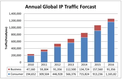
Figure 2.2: IEEE802.3 100Gb/sbackplane insertion loss (Data is from IEEE website).
Figure 2.2 plots the insertion loss versus signal frequency of a typical IEEE802.3 100Gb/s
backplane with different substrate materials and trace lengths [18]. The insertion losses at
Table 2.1: Inerstion Loss (IL) comparison of different channels. Channel Type Length(inch) IL at 10GHz(dB) IL at 20GHz(dB)
Nelco4000-6 42.8¨ -39.9 -79.3
Megtron-6 42.8¨ -22.6 -43.3
Nelco4000-6 29.8¨ -28.1 -57.2
Megtron-6 29.8¨ -16.2 -32.2
backplane may have huge insertion loss which could exceed 80dBat half of the signal data
rate. In effect, this frequency dependent loss tends to attenuate signal with high frequency
pattern such as 01010101 more than the low frequency pattern such as 111000111 and
leads to ISI or Data-Dependent Jitter which limits the range of communication.
There are 3 major causes of insertion loss in the copper channel:
1. Skin effect (IL(dB)∝√F requency)
2. Surface roughness (IL(dB)∝F requency)
3. Dielectric loss (IL(dB)∝F requency)
as denoted in Figure 2.3.
Metal
Metal
Depth
AC Current Density
f1>f2
Metal
(A) (B) (C)
Figure 2.3: Causes of copper channel loss: (A) Skin effect. (B) Surface roughness. (C) Dielectric loss
Skin effect confines the high frequency AC current to flow only in a thin layer on the metal
surface which increases the effective resistance of the channel. The surface roughness
exaggerates the skin effect by increasing the total signal path’s length. The molecules of
the dielectric material usually have more or less the dipole moments due to asymmetric
rotating these dipoles dominates the loss at higher frequency since it is proportional to the
signal frequency.
To address the loss issue, equalization technique, at both the transmitter and the receiver
side, has been employed intensively which tries to compensate the signal distortion of
the communication channel by making the overall frequency response as flat as possible.
Nevertheless, these techniques are still facing a lot of challenges such as high power
consumption, increased chip area, cost and complexity, susceptible to process, voltage,
and temperature (PVT) variations in an analog equalizer, and stringent timing requirements
in a digital equalizer etc.
Another approach to tackle the loss issue is to reduce the symbol rate by implementing
a multi-level modulation scheme such as PAM-4(Pulse-amplitude modulation with 4
lev-els) [19] where the symbol rate is only one half of the data rate. While PAM-N (N is the
number of levels) achieves a symbol rate reduction oflog2N from the data rate, it has the
drawbacks of requiring anlog2N-bit DAC (digital-to-analog converter) and anlog2N-bit
AD-C (analog-to-digital converter) on both sides of the interconnect as well as reduced SNR
performance. The symbol rate can also be kept low by running multiple wires in parallel.
However, it is difficult to align the parallel data to clock at high frequency due to mismatch.
Furthermore, when integrating so many transceiver into a small area, the heat generated
by these circuitry could be prohibitively high for the system to function properly.
While the use of parallel wires for data and address could mitigate the loss problem and
increases the link capacity to a certain extent, the crosstalk arises from the parasitic
capac-itance between wires which is another severe issue of metal interconnect. Crosstalk not
only increases the chance of data error but also consumes more power while charging and
discharging the parasitic capacitance. To maintain the signal integrity, differential signaling
or shielded wire are widely used while both of them will reduce the link density and incur
2.1.3. Optical Interconnect
When an electrical channel is reaching its fundamental limits such as bandwidth and
dis-tance, optical links, on the other hand, are far from those limits. Optical fiber
communica-tion has several major advantages over convencommunica-tional electrical links.
1. Very long link distance and extreme high data rate
2. Thinner,lighter and low cost
3. No crosstalk issue
An optical link can be treated as a wireless channel with carrier frequency many
thousand-s of timethousand-s higher than thothousand-se of microwave electrical carrierthousand-s (about 194T Hz for 1.55µm
wavelength) which provides ample bandwidth for data. With the help of wavelength-division
multiplexing (WDM), the optical equivalent of frequency-division multiplexing, one
opti-cal fiber can transmit multiple carriers simultaneously. In addition, advanced modulation
schemes such as pulse amplitude modulation (PAM), quadrature phase-shift keying
(QP-SK), and polarization-division multiplexing further increase the link capacity. Link speed
of 112Tb/s over a 76.8km7-core fiber has been achieved with 160 107Gb/schannels per
fiber [20]. As transmission technology advances, higher bandwidths are possible over
the same optical fibre links without having to replace the cables. Thanks to the extremely
low loss fiber and low noise optical amplifier, the optical signal can be transmitted over
12,000km at 495Gb/s [21]. The optical fiber core, usually made ofSiO2 or glass with a
diameter of 125µm, is cheaper and lighter than copper. More importantly, optical fibre is
immune to electro-magnetic interference due to the dielectric nature of the fiber materials,
and so is ideal for environments where there is high voltage equipment nearby.
Even though an optical link provides unsurpassable link speed and distance over electrical
link, its disadvantages should also be mentioned:
optical links, when considering the transmitter, receiver, repeater, and etc., are still
more expensive than copper. The commercial product are also bulky and power
hungry in order to meet the stringent specifications of the telecom market.
2. Fragility - Optical fibre can’t be bent too much otherwise it will break.
3. Sensitive to chemicals -SiO2 property can be affected by various chemicals such as
hydrogen gas in underwater environment.
4. Opaqueness - Most fibers become hard and opaque when exposed to Nuclear
radi-ation.
5. Hard to maintain - Optical fibres cannot be connected together as a easily as copper
wire.
For these reasons, optical links are mostly found in long haul applications where capacity
and distance were big concerns prior to 2000.
In summary, the choice among wireless, electrical, optical fiber or other technologies for a
particular system is based on a number of trade-offs. There is no single solution can serve
all applications needs.
2.2. Optical Communication Overview
Optical communication has a long history which can go back to more than 2000 years ago.
At that time, people in ancient China, Greece and Egypt once used mechanical methods
to modulate the light including smoke signals, fire beacons, and optical telegraphs [22]
some of which are still being used today in some emergency situations. These
approach-es, which are referred to as free-space optical communication now, can not achieve a very
high data rate due to its mechanical nature. The distance is also subject to environmental
conditions such as fog, rain and day light. Lacking of techniques to tackle these issues,
their positions in real time, long distance communication were soon replaced by electrical
twen-tieth century , during which period extraordinary scientific progresses had been made in
the electromagnetic theory, generation and detection of radio signals, new materials, and
elemental electronic devices etc.
Due to lack of capable technologies to generate, modulate, and detect the the light, the
evolution of optical communication seems to stop until the 1950s. In 1958, the major
breakthrough of optical communication, laser, was first invented [6] after its theoretical
foundations being established by Albert Einstein almost 40 years before [23]. After that,
optical communication embraced its golden age with the explosive discoveries and
ad-vancements in the areas of light sources, light detectors, material’s interaction with light,
low loss optical transmission medium, integrated circuits and etc.
Shortly after the invention of the laser, the semiconductor laser diode was successfully
demonstrated [24] followed by the high speed avalanche photo detector [25]. In the mean
time, extensive research had been carried out to study the material electro-optic
proper-ties which can be potentially used to modulate light. In fact, the first optical modulators
based on electro-optic effect was introduced almost the same time as the ruby laser was
invented [26]. For the optical fiber, the major medium in optical links, the fiber loss has
been reduced from the early date of 20dB/km [27] to about 0.15dB/km [28] at the
low-loss window around 1.55µm. In addition, to compensate for the fiber loss, Erbium-doped
fiber amplifier (EDFA) was invented [29] which greatly extended the optical link reach.
Ad-vanced modulation and multiplexing schemes, such as QAM, DWDM, OFDM (orthogonal
frequency-division multiplexing), and PolPSK (polarization multiplexing phase-shift keying),
have been developed to sustain the increasing demand for bandwidth.
After almost 60 years of intensive developments, a global optical network infrastructure
has been established responsible for carrying virtually all telephone calls and internet
traf-fics. Initially, fiber networks were mainly deployed for long-haul or submarine transmission
because it offers unparallel reach and bandwidth product. In the mean time, the explosive
even into individual homes. For short reach applications such as HPC, there is also a trend
of replacing the interconnect, historically dominated by copper wire, with optical links at all
levels from local area network (LAN) and rack to rack, to board level or even inter chip
interconnect [5]. In these domains, traditional optoelectronics interconnects have some
serious issues in terms of power consumption, link density and cost. For example, the IBM
Roadrunner supercomputer has 57 miles of cable and consumes nearly 3 megawatts of
power, almost 15% ∼23% of which is contributed by the interconnects [2]. The existing
optical transceiver module is also bulky and expensive which usually costs a few thousand
dollars for a 10Gb/smodule. To meet the future needs of HPC, the price of optical link has
to be cheaper than $1/Gb/sand the power efficiency has to be better than 5mW/Gb/s[30].
It also needs to be compact such that hundreds of links can fit into a small space.
2.2.1. System Architecture
When people talk about optical communication, most of them refer to the long-haul fiber
network which spreads globally. To increase the capacity, dense wavelength division
mul-tiplexing (DWDM) is intensively employed in today’s optical links, in which more than a
hundred wavelengths carrying 10Gb/s or more data are combined into a single fiber of
125µmin diameter [20, 31, 32].
Laser λ1 Modulator
MUX Laser λn Modulator
Fiber
Amplifier
Information
Information
DE MUX
Detector λ1
Detector λn
Figure 2.4: System diagram of a DWDM optical link.
Figure 2.4 shows the system diagram of a typical DWDM optical link. In this system, digital
information such as audio, video and data is first converted to optical power through the
external modulator which is known as electrical to optical converter, or E/O converter. The
optical input of the modulator comes from laser sources with different wavelengths (e.g.
modulated by the information to generate the desired output. All the outputs from the
mod-ulator are then merged into a single strand of fiber via the optical multiplexer (MUX). After
the light travels a long distance in the fiber, it may suffer from loss, chromatic dispersion
and polarization mode dispersion which require optical amplifier or repeater to regenerate
the signal before it reaches the receiver. On the receiver end, after de-multiplexing
(DE-MUX), lights with different wavelengths are sensed by the photo detector and converted
back to electrical signal (optical to electrical conversion, or O/E). This electrical signal is
then processed, which may include reconditioning the signal in the analog domain and
restoring the clock in the digital domain, to recover the original information.
One of the key building blocks in the optical link is the modulator or the transmitter since it
directly impacts the performance of the link such as capacity, reach, power consumption,
receiver design, and in some applications the cost. In the past 60 years, tremendous
research efforts have been spent in the areas of material, electrical circuit, and fabrication
process etc. to develop the E/O converter in order to meet these performance requests.
The focus of this work is to design a high performance optical transmitter by leveraging the
novel modulator technologies developed by CISCO Systems.
In real systems, there are also other additional blocks to make the link more robust. For
example, a temperature control unit is required for the laser source to keep the wavelength
stable especially in the DWDM system where the channel spacing is so small (0.8nmwith
100GHz channel spacing). In the polarization division multiplexing DWDM, a polarization
detector is necessary to de-multiplex the signal. Also, when the optical power exceeds the
working range of the detector, a variable optical attenuator (VOA) is needed.
Although optical links other than this long-haul network may have slightly different
topolo-gies, their fundamental building blocks and system scheme, as mentioned above, are
2.2.2. Modulation Format and Spectral Efficiency
Analogous to electrical wireline or wireless communication, the physical signals in
opti-cal communication could have multiple forms. Although continuously changing intensity
of light can carry information such as TV signal [33], it is susceptible to noise,
nonlin-earity of fiber and other non-ideal factors due to its analog nature and is rarely used in
commercial products. On the contrary, digital modulation formats don’t demonstrate these
drawbacks because they map information into discrete digital status. Thus, digital
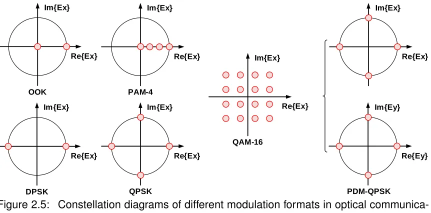
modula-tion formats are the primary choices in fiber links. The constellamodula-tion diagrams of different
digital modulation formats are illustrated in Figure 2.5. On-off keying (OOK), as a two-level
Im{Ex}
Re{Ex}
OOK
Im{Ex}
Re{Ex}
DPSK
Im{Ex}
Re{Ex}
PAM-4
Im{Ex}
Re{Ex}
QAM-16
Im{Ex}
Re{Ex}
Im{Ey}
Re{Ey}
PDM-QPSK Im{Ex}
Re{Ex}
QPSK
Figure 2.5: Constellation diagrams of different modulation formats in optical communica-tions.
amplitude-shift keying (ASK), is probably the simplest form in optical links where the binary
information is represented by the presence and absence of light which can be expressed
by the amplitude of the electric field (Ex) or light intensity (∝Ex2). Owing to its simplicity,
OOK was exclusively adopted by digital optical networks prior the year of 2000. It is
ac-tually the first format being employed in 40Gb/scommercial product [34] and in 100Gb/s
research project [35]. OOK has a spectral efficiency (SE) of 1b/s/Hz. To increase the SE,
digital message is encoded to multiple intensity levels resulting in N-level pulse-amplitude
number of levels.
Phase-shift keying (PSK), in which digital signals are mapped to different phases of the
carrier — light, is another important modulation form in optical links. Several schemes
exist for PSK such as binary phase-shift keying (BPSK) — the basic 2-level PSK,
differen-tial phase-shift keying (DPSK) — the differendifferen-tial version of BPSK, quadrature phase-shift
keying (QPSK) — BPSK in quadrature form, and n-PSK — multi-level PSK. Similar as in
PAM-N, the SE in PSK is determined by the number of phases. Because the error rate can
not be well controlled, higher order PSK than 8-PSK is seldom implemented.
As demand for bandwidth continuously increases, high order quadrature amplitude
modu-lation (QAM) is developed in which PAM-N is applied to two carriers (lights with the same
wavelength) 90◦ out of phase (quadrature phase). The result waveform is called QAM-N2 with a SE of Nb/s/Hz.
To further increase the SE, polarization is another parameter to leverage. Since the linear
polarizations, Ex and Ey, are orthogonal, the information contained in each polarization
direction is resolvable at the receiver after polarization filters. Combining this
polarization-division multiplexing (PDM) with other modulation techniques, the SE is easily doubled.
Performances of some recently developed PDM systems are summarized in Table 2.2.
Table 2.2: Recent development of PDM systems.
Format Baud rate (GBaud/s) Data rate (Gb/s) Reference
PDM QAM-256 4 64 [36]
PDM QAM-32 10 93 [37]
PDM QAM-64 9.3 112 [38]
PDM QPSK 56 224 [39]
There are also other formats available such as frequency-shift keying (FSK) and orthogonal
frequency-division multiplexing (OFDM) which can be thought as a special type of WDM
by encoding data into different frequencies.
real SE, as determined by Shannon’s “Theory of Information” [40], is always smaller due
to noise.
2.3. Light Fundamental
To effectively control the light, a profound knowledge of its fundamental properties is
es-sential. Among all kinds of light, laser is virtually the solo source of all commercialized
optical communication systems because it has high coherence, very pure spectrum and
high directionality. This section starts by introducing the basic properties of light. Then, the
physical effects of material which influence these optical properties will be given.
2.3.1. Light Property
Light/laser exhibits both wave and particle properties which is known as wave-particle
du-ality, a central concept of quantum mechanics.
While considering its wave property, light is a type of electromagnetic wave following
Maxwell equations (2.1) - (2.4):
∇ ·D=ρ (2.1)
∇ ·B= 0 (2.2)
∇ ×E=−∂B
∂t (2.3)
∇ ×H=J+∂D
∂t (2.4)
whereEand Hare the electrical and magnetic field,D =εE,B =µH, andJ =σEare
called the constitutional relations. The permittivityεand permeabilityµare related to the
relative permittivityεr and relative permeabilityµr byε =ε0εr and µ=µ0µr respectively.
For nonmagnetic medium, which is true for most optical devices,µris one.
non-conductive medium (ρ=0, σ=0) along z-axis, the general solution for the electrical
field can be expressed as
E=E0ej(kz−ωt) (2.5)
where
k=pεµ0ω2 (2.6)
is defined as the propagation constant andω is the frequency of light . The speed of light
in the medium can then be written as
v= ω k =
c nRI
(2.7)
wherec= √1
ε0µ0 is the velocity of light in free space,nRI is the refraction index (RI) of the
medium. Thus
nRI =
ck
ω =
√
εr (2.8)
which is a real quantity. However, the refractive index is complex in general because of loss
in the material. Without loss, light will propagate in the medium with constant amplitude
as shown in (2.5). In reality, materials exhibit dielectric loss at high frequencies because
the polarization status can not respond fast enough to an applied field. In addition, ideal
insulator with σ = 0 doesn’t exist. Considering both aspects, loss can be modeled by
permittivity that is both complex and frequency dependent as
ε(ω) =εR(ω) +jεI(ω) (2.9)
To be noted that,εRandεI are related to each other by the Kramers-Kronig equation
εR=
1 πP
Z +∞
−∞ εI(ω
0
)dω0
ω0 −ω (2.10)
εI =−
1 πP
Z +∞
−∞ εR(ω
0
)dω0
ω0−ω (2.11)
Thus, the refractive index becomes a complex number which can be defined as
From (2.8) and (2.12),ε(ω)is related tonRI(ω)by
εR=n2R−n2I (2.13)
εI= 2nRnI (2.14)
Now, the propagation constant becomes
k= nRω c +j
nIω
c (2.15)
The electrical field can now be expressed as
E=E0e−
nIωz
c ejω(
nRz
c −t) (2.16)
Therefore, the electric field is attenuated exponentially as
|E|=E0e−
nI ωz
c =E0e−
1
2αz (2.17)
whereα = 2nIω
c is the absorption coefficient or loss coefficient. The factor 1/2 is added in
(2.17) simply because the loss is conventionally defined for intensity which is proportional
to the square of the electric field and can be written as
I(z) =I0e−αz (2.18)
While considering its particle property, light is composed of discrete photons, an
elemen-tary particle, which is the quantum of light. Each photon possesses a frequency dependent
energy
Ephoton=
hc
λ (2.19)
wherehis Planck constant andλis the light’s wavelength.
A close examination of (2.16) reveals there are multiple properties of light that can be used
to carry message.
Amplitude
Nearly all commercially available optical links use the amplitude to carry information. From
(2.16), the amplitude of the electric field is E0e
−nIcωz
![Figure 2.10(B). According to the empirical equation from [56], the transmittance of the](https://thumb-us.123doks.com/thumbv2/123dok_us/9323936.1467206/58.612.148.497.119.372/figure-b-according-empirical-equation-transmittance.webp)