Review
1
Infra-Red Plasmonic Sensors
2
Anthony Centeno 1,2,3,*, Siti Rahmah Aid2 and Fang Xie 3
3
1 Department of Electrical and Electronic Engineering, Xi’an Jiaotong Liverpool University, 111 Ren’ai Road,
4
Suzhou Dushu Lake Higher Education Town, Jiangsu Province, China, 215123
5
6
2 Department of Electronic Systems Engineering, Malaysia Japan International Institute of Technology,
7
University Technology Malaysia, 54100, Kuala Lumpur, Malaysia; [email protected]
8
3 Department of Materials, Imperial College London, Exhibition Road, London, UK. SW7 2AZ;
9
10
* Correspondence: [email protected]; Tel.: +86 512 81884766
11
Abstract: Plasmonic sensors exploiting the Localized Surface Plasmon Resonance (LSPR) of noble
12
metal nanoparticles are common in the visual spectrum. However, for bio-sensors the near
infra-13
red (NIR) windows (600 nm – 900 nm and 1000 nm -1400 nm) are of interest, as it is a region where
14
the absorption coefficient of water, melaninm deoxy- and hemoglobin are all low. The first part of
15
this paper reviews the work that has been undertaken on using gold (Au) and silver (Ag) particles
16
in Metal Enhanced Fluorescence (MEF) in the NIR. Despite this success there are limitations, as there
17
is only a narrow band in the visual and NIR where losses are low for traditional plasmonic materials.
18
Further, noble metals are not compatible with standard silicon manufacturing processes, making it
19
challenging to produce on-chip integrated plasmonic sensors with Au or Ag. Therefore, it is
20
desirable to use different materials for plasmonic chemical and biological sensing, that are
foundry-21
compatible with silicon (Si) and germanium (Ge). One material that has received significant
22
attention is highly doped Ge which starts to exhibit metallic properties at a wavelength as short as
23
6 μm. This is discussed in the second part of the paper and the results of recent analysis are included.
24
Keywords: NIR; Plasmonics; LSPR; MIR; Germanium
25
26
1. Introduction
27
At the interface between materials with different signs for the real part of the permittivity Surface
28
Plasmon Polaritons (SPP) can be excited. The requirements for the negative permittivity material is
29
normally undertaken by noble metals, gold (Au) and Silver (Ag). Since the wave is on the boundary
30
of the metal and an external medium it is very sensitive to any change of this boundary. The excitation
31
of surface plasmons by light is termed surface plasmon resonance. The resultant resonant interaction
32
between the SPP and the metal surface results in a significantly enhanced electromagnetic near-field
33
[1]. SPP exhibit many applications in subwavelength optics, including chemical sensors and
34
biosensors [2,3].
35
If Au or Ag nanoparticles, of dimensions much smaller than the wavelength of excitation, are
36
considered incident light can excite Localised Surface Plasmons (LSP), where the charge density
37
oscillations are confined to the metallic particles. An external field is able to displace the free electrons
38
in the nanoparticle, with respect to the fixed ionic core [1]. This displacement sets up a restoring force
39
leading to coherent oscillations of the charge density, hence, a resonant frequency. This is termed
40
Localised Surface Plasmon Resonance (LSPR).
41
One application that exploits the LSPR, which has received much attention for the purpose of
42
bio-sensing, is Metal Enhanced Fluorescence (MEF) [4-22]. MEF is now a well-recognized technology
43
wherein the near-field interaction of fluorophores with metallic nanostructures can lead to
44
substantial fluorescence enhancement.
45
Fluorescent molecules emitting at wavelengths in the infra-red window, in which penetration
46
depth is high and autofluorescence minimum are of particular interest and are potentially an
47
attractive technology for bio-applications [20]. However, the low quantum yield and poor
48
photostability of NIR dyes currently limits their applicability. To design and synthesize Near
Infra-49
red (NIR) dyes with high quantum yield and photostability has proved to be extremely challenging,
50
due to the complex synthetic routes required for these large, complex molecules [20]. The
51
amplification of light from NIR fluorophores by MEF is a promising strategy for dramatically
52
improving both the detection sensitivity and image enhancement, thereby realizing the potential
53
advantages of the NIR fluorophores. Section 2 of this paper discusses the physical process of MEF
54
and reviews some of the published work by the authors.
55
At the NIR loses arise in Au and Ag from intraband (or Drude) losses. There is, therefore, only
56
a narrow band in the visual and NIR where losses are low for traditional plasmonic materials. A
57
further challenge associated with noble metals is that they are not compatible with standard silicon
58
manufacturing processes. Further, Nobel metals diffuse into the semiconductor forming deep level
59
traps which have an adverse effect on device performance. Whilst Au and Ag are the obvious choice
60
for visible and NIR applications there is a desire and need for chemical and biological sensing in the
61
mid-infrared (MIR) [22-24] using materials that are foundry-compatible with silicon (Si) and
62
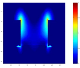
germanium (Ge), that might lead to on-chip integration of devices governed by plasmonic effects
63
[25,26]. One material that has received significant attention as a potential plasmonic material in the
64
MIR is highly doped Ge [22, 25, 26]. In section 3 of this paper we explore the advantages of highly
65
doped Ge as a MIR plasmonic material. By analysing data available in the literature for doped Ge
66
thin-films we discuss, using computational electromagnetics, some of the fundamental issues related
67
to future applications and exploitation.
68
2. Metal Enhanced Fluorescence in the Near Infra-Red
69
MEF can be considered a three stage process [17]. The first is the increased absorption of exciting
70
light by the dye molecule due to the enhanced electric field around the nanoparticle caused by the
71
LSPR. Once in an excited state the molecule undergoes internal processes to bring it into the emitted
72
excited state. Although the metal can modify these processes they are very fast compared to the
73
other two processes, and are not usually considered in the analysis of the MEF mechanism. Finally
74
the molecule decays, through the emission of a photon, to the ground state. The metal will modify
75
the radiative decay rate and create new channels of non-radiative decay, through energy and charge
76
transfer between the molecule and metal.
77
The fluorescence rate, Ψ, is the product of the excitation rate, γe, and the quantum yield, q. At
78
the excitation wavelength of the molecule, λex, the incident light irradiates the metal nanoparticle and
79
the near-field around the particle excites the emitter. At the emission wavelength, λem, of the
80
fluorophore it behaves as an oscillating dipole. Since it is in the proximity of the metal nanoparticle
81
the radiated emissions from the fluorophore, and hence the quantum yield, are modified [27].
82
The quantum yield of an isolated fluorophore molecule is [27]:
83
84
0 0
0 0
nr r
r
q
γ
γ
γ
+
=
(1)85
86
whereγ0r and γ0nrare the radiative and non-radiative decay rates respectively. The superscript 0
87
indicates the fluorophore is isolated, rather than in the presence of a metal nanoparticle.
88
In the presence of a metallic particle there will be additional radiative and absorption channels,
89
giving a modified quantum yield [28]:
90
91
0 nr m abs m r
m r m
q
γ + γ + γ
γ
= (2)
Considering a single fluorophore coupled to a nanoparticle to obtain values of modified
93
quantum yield and fluorescent rate enhancement. This requires calculating the decay rates,
γ
rm, m absγ
94
and
γ
r0by considering the spontaneous emission of the fluorophore as a small electric dipole [28].95
These decay rates can be found in terms of the Poynting vector, as described in reference [28] such
96
that:97
98
(
)
2 da Re s * r
× = γ T T H E (3)99
100
and101
(
)
2 da Re s * m abs
× − = γ S S H E (4)102
103
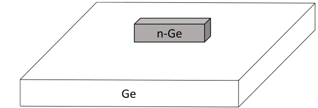
where s is a surface that encloses the fluorophore molecule (small dipole) and nanoparticle. In
104
equation (6) we consider the total electric and magnetic field crossing s, whereas in equation (7) it is
105
the scattered fields from the nano-cylinder that are considered, hence the subscripts T and S. To find
106
0 r
γ
from equation (6) only the small dipole has to be considered in the calculation, whilst to find107
m r
γ
the metal nano-cylinder is added to the model and enclosed by the surface.108
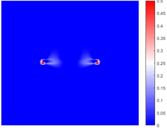
The excitation rate is found by considering the local electric field at the position and wavelength
109
of excitation, E(xd, λex) and the emitters orientation ep . If we consider the electric field in the presence
110
of the metal nanoparticle near the fluorophore molecule, then the excitation rate enhancement is [29]:
111
112
2 2 ex d 0 e m e | | | ). , x ( | i p E e E λ = γ γ =χ (5)
113
where Ei is the free space electric field (incident field) without the nano-cylinder being present.
114
The fluorescent rate enhancement, Ψenh, can now be found from:
115
116
0 m enh q q . χ =Ψ (6)
117
118
From Equations (1)-(6) it is possible to calculate the emission enhancement from a fluorophore
119
in close proximity to metal particle using computational electromagnetics [1, 28, 29].
120
Figure 1 shows the electric field enhancement around cylindrical nanoparticles for an incident
121
plane wave of wavelength 650 nm. It can be seen that in most of the gap the magnitude of the electric
122
field exceeds that of the incident field (The scale is logarithmic). This leads to excitation enhancement
123
of fluorophores in this region. In the proximity of the corner, at the top of the nano-cylinder, the
124
magnitude of the near-field is seen to exceed that of the incident field by 2 orders of magnitude.
125
Previously published work used Finite Difference Time Domain (FDTD) analysis to calculate both
126
the excitation and emission enhancement of fluorophores. The results showed that it is important, for
127
the maximum fluorescent rate enhancement that the excitation and wavelengths of the dye should
128
130
131
Figure 1. Electric field in the gap between two cylindrical nanoparticles. The electric field magnitude is
132
normalized to the magnitude of the incident field. (Note the scale is logarithmic from 0(dark blue) to 2 (dark
133
red))
134
135
The NIR windows (600 nm – 900 nm and 1000 nm -1400 nm) are of interest as it is a region
136
where the absorption coefficient of water, melaninm deoxy- and hemoglobin are all low. Most of the
137
reported work on MEF for the enhancement of NIR fluorescent dyes are based on gold nanostructures
138
including nanorods, nanoshells and porous Au films by dealloying [20]. This is primarily because Au
139
has a lower plasma frequency than Ag, so the LSPR peak is at a longer wavelength, as well as having
140
a higher chemical stability. However, Ag can be an attractive material since it has a lower absorption
141
efficiency and a higher scattering efficiency. This leads to larger field enhancement at the LSPR,
142
leading to a larger excitation enhancement in MEF. The LSPR is dependent not just upon material but
143
also on the shape of the nanoparticle, and MEF has been successfully demonstrated in the NIR using
144
triangular-like Ag nanoparticles immobilized on glass substrate [19, 20], nanocylinders [15] and
145
Nanostar [16]. Table 1 summarizes some of the results presented in published work by the Xie group
146
at Imperial College for MEF in the NIR, for both Au and Ag nanoparticles, for excitation wavelengths
147
up to 780 nm.
148
149
Table 1. Metal enhanced fluorescence in the near infra-red using Au and Ag nanoparticles
150
Fluorophore Excitation wavelength
(nm)
Emission wavelength
(nm)
Fluorescent Enhancement
Type of Nanoparticle
Reference
AF 790 780 790 68.8 Au,
Nanotriangle
[19]
AF 790 780 790 83 Ag,
Nanotriangle
[20]
AF 750 730 750 235 Au, Cylinder [15]
AF 750 730 750 321 Au, Nanostar [16]
AF 790 780 790 195 Au, Nanostar [16]
Ag2QD 780 1205 40 Au, Nanostar [16]
151
3. Ge as a Plasmonic Material in the Mid Infra-Red
152
Germanium (Ge) is a promising material for replacing silicon as a substrate for MOS devices.
153
Further downscaling of silicon based devices will lead to the Short Channel Effect (SCE) that will
154
result in an increase in the leakage current [30-32]. This leakage current will increase the power
155
consumption of devices, whilst also reducing the performance. High drive current capability of
156
devices without further downscaling process can be realized by increasing the carrier mobility in the
157
transistor, due to its higher electrical carrier mobility (3900 cm2/ V.s for electrons and 1900 cm2/ V.s
159
for holes) [30]. Furthermore, its similarity with conventional Si will ease the replacement process in
160
manufacturing lines. It would therefore be very attractive if plasmonic sensors could be based on Ge
161
for on-chip integration.
162
To consider this further we can start from the free electron response in metals, given by the
well-163
known Drude model:
164
ω
γ
ω
γ
ω
γ
ω
ω
ε
ωγ
ω
ω
ε
ε
ε
ω
ε
)
(
''
'
)
(
2 22 2 2 2 2 2
+
+
+
−
=
+
−
=
+
=
∞ ∞ p pi
i
p (7)165
Where ε∞ is the high frequency relative permittivity, ωp is the plasma frequency and γ is the
166
Drude relaxation rate.
167
The optical response of free carriers is described by equation 7. If we consider the real part and
168
define a cross-over frequency, ωc, where the real part becomes zero, we get:
169
170
)
(
2 22
ε
ω
γ
ω
p=
∞ C+
(8)171
Rearranging (8) gives:
172
173
2 2γ
ε
ω
ω
=
−
∞ pc (9)
174
This is the shortest wavelength where the semiconductor can exhibit metal like properties that
175
is have a negative real part of permittivity. The required free carrier concentration, n, in the
176
semiconductor for a cross-over frequency can be found from [26]:
177
178
2 0 * 24
e
m
n
pπε
ω
=
(10)179
180
Where ε0 is the free space permittivity, m* is the effective mass of the carrier and e is the electron
181
charge.
182
As can be seen the higher the free carrier concentration the higher the cross-over frequency. It
183
should be noted here that in the literature it is often assumed that the plasma frequency and the
cross-184
over frequency are the same. In fact this is only the case for the lossless case where γ=0 and if
185
interband transitions are ignored (ε∞ =1). This is discussed in depth by Frigerio et al [26]. To fit the
186
Drude model to the dielectric function the value of ε∞ is approximately the dielectric constant of
187
undoped semiconductor in the MIR (≈16 for Ge).
188
In the visual-NIR the analysis and design of plasmonic devices requires accurate determination
189
of the dielectric function. This is then used to find the electromagnetic field, or find the dispersion
190
relation, using computational electromagnetics. To do this the parameters ε∞, ωp, and γ need to be
191
found and applied in an electromagnetic simulation. The parameters can be found by using a
192
multilayer based model to calculate the reflectance from the doped Ge film and iteratively modifying
193
the parameters to obtain a good fit to measurements. These can be obtained in the MIR using Fourier
194
Transform Infra-Red (FTIR) spectroscopy (rather than UV-VIS-NIR spectroscopy). The calculation of
195
reflection can be done using the transfer matrix method [33] [see for example the code from Steven
196
Byrnes at http://sjbyrnes.com]. However, since the reflectivity measurements are made on a thin film
197
it is very fast to calculate reflection using a Finite Difference Time Domain (FDTD) model, as the only
198
spatial discretization required is in the direction of the incident plane wave, which is normal in this
199
In this work we have first considered published data from Frigerio et al [26] and Prucnel et al
201
[22]. In both cases we derive the Drude model from their experimental data. We also fit data from
202
FTIR measurements we have undertaken on Ge thin films manufactured using Ion Implantation and
203
rapid laser annealing [30].
204
Frigerio et al [26] have considered heavily doped films produced using a
low-energy-plasma-205
enhanced Chemical Vapor Deposition (CVD) reactor, using phosphorus as the n-type dopant. They
206
present the dielectric functions for samples with carrier densities (η) up to 3.0x1019 cm-3. We have then
207
used the RefFIT code [35] to extract the parameters for the Drude model for two samples, shown in
208
Table 2. These are then used in an FDTD code [36] to calculate the extinction properties and electric
209
field enhancements.
210
211
Table 2. Drude parameters for Phosphorus doped Ge derived, from Figure 7, ref [26] using ReFIT [35]
212
The thickness of the Ge films reported in [26] are 2 μm.
213
Material number
η (cm-3) ε∞ ωp (cm-1) ωc (cm-1) γ (cm-1) Sample
number in ref [26]
1 2.3x10¹⁹ 16.5 4032 974.3 189.83 9338
2 3.0x10¹⁹ 16.2 4705 1147.4 224.64 9336
214
Using these parameters we have investigated the sprectral response of a rectangular prism
215
doped (n-Ge) particles sitting on an un-doped Ge substrate, as depicted in Figure 2. Figure 3 shows
216
the absorption, scattering and extinction for a particle that is 2 μm long, 1 μm wide and 1 μm high. It
217
can be seen that there are two extinction peaks, one at 490 cm-1 (wavelength of 20.4 μm) and the other
218
at 1050 cm-1 (9.523 μm).
219
220
221
Figure 2. Phosphorous doped, n-type germanium particle on a germanium substrate.
222
223
n-Ge
224
Figure 3. Spectral response for rectangular prism n-Ge particle (material 2 in Table 2) calculated using FDTD.
225
Height 1 μm, length 2 μm, width 1 μm.
226
227
Considering the extinction peaks in Figure 3 it can be seen that the lower frequency peak,
228
although predominantly absorption, also has a significant scattering content. On the other hand the
229
higher frequency peak is absorption dominated. Figure 4 shows the electric field enhancement at both
230
frequencies. It can be seen from Figure 4(a) that at 490 cm-1 the peak field enhancement is 2 orders of
231
magnitude at the corners of the n-Ge particle, at the interface with the Ge substrate. Nevertheless at
232
least an order of magnitude (x10) enhancement is seen around the sides of the particle. In contrast
233
the field enhancement is much lower at 1049 cm-1, with a maximum of 1 order of magnitude very
234
close to the n-Ge surface. The sensitivity of an LSPR sensor is related to the increased electric field
235
enhancement around the particle.
236
237
238
(a) (b)
239
Figure 4. Electric field enhancement the extinction peaks of 1 μm high n-Ge particle. The excitation is (a) 490 cm
-240
1 and (b) 1049 cm-1respectively. The scale is logarithmic and the electric field enhancement is normalized to the
241
incident electric field. The plots are for a cross-section through the centre of the particle (mid-width). (The
242
incident field is normal to the top surface of the particle and polarized in the length direction.)
243
244
The height of the n-Ge particle considered in the model was reduced to 0.5 μm and 0.1 μm,
245
respectively. The spectral response is shown in Figure 5 for both FDTD calculations. It can be seen
246
particle, whilst for the 0.1 μm case there is only a single observable peak, which is caused almost
248
totally by absorption.
249
250
(a) (b)
251
Figure 5. Spectral response for rectangular doped Ge particles (material 2 in Table 2) for (a) height 0.5 μm and
252
( b ) h e i g h t 0 . 1 μm . T h e l e n g t h i s 2 μm a n d t h e w i d t h i s 1 μm i n b o t h c a s e s .
253
254
The electric field enhancement for the 0.1 μm high n-Ge particle at 651 cm-1 is shown in Figure
255
6. The enhancement is much less than 1 order of magnitude and strongly confined to the sides of the
256
particle. This suggests that the use of n-Ge as LSPR sensors is limited by their height.
257
258
Figure 6. Electric field enhancement for extinction peak of 0.1 μm high n-Ge particle. The scale is logarithmic
259
and the electric field enhancement is normalized to the incident electric field.
260
A higher carrier (doping) density is obtainable using ion implantation and annealing. Prucnal et
261
al [22] achieved carrier concentrations of ~2.2 x 10²⁰ using rear side flash-lamp annealing (r-FLA). This
262
gave n-Ge films of thickness 140 nm. In our analysis, based on their reflection measurements, this
263
gave a ωc of 1850 cm-1 (wavelength = 5.4 μm). Our group has produced n-Ge films from ion
264
implantation and rapid laser thermal annealing [30]. The thickness of these films is between 40 and
265
90 nm on a Ge substrate. FDTD models were used to replicate the reflection obtained from FTIR
266
measurements. From this analysis it was found that an n-Ge film had the following Drude
267
parameters; ωp = 6500 cm-1, ε∞ = 16.5, γ = 241 cm-1. The comparison between the experimental and
268
fitted results is shown in Figure 7. The analysis gives a ωc of 1582 cm-1 (wavelength 6.3 μm) and a
269
carrier concentration of 5.5 x 1019 cm3. (Reference [30] should be referred to for further discussion of
270
the fabrication process)
271
273
Figure 7. Measured and modelled reflection from an n-Ge thin film of thickness 40 nm, and ωc 1582 cm-1.
274
275
These results show that n-Ge films can be produced with large carrier concentrations and
cross-276
over wavelengths around 6 μm. Unfortunately, the thickness of the films is only of the order of 100
277
nm, or less, too thin to support large field enhancement from the LSPR of a particle. Nevertheless, it
278
may be possible that the thin film can be used to support propagating surface plasmon polaritons for
279
a plasmonic MIR sensor. The production of n-Ge films, with a high ωc, is an important first step along
280
this path but significant research is needed in the future to produce integrated plasmonic sensors.
281
4. Discussion and Conclusion
282
In this paper we have discussed the application of the Localised Surface Plasmon Resonance to
283
infra-red chemical and biological sensors. Using Metal Enhanced Fluorescence (MEF) it has been
284
demonstrated that traditional palsmonic materials, Au and Ag, can be used in the NIR window. The
285
excitation wavelength of the LSPR, though, is limited to short wavelengths in the NIR (~ 780 nm) as
286
intraband (or Drude) losses become increasingly large. In addition, it would be very attractive to have
287
on-chip integration of plasmonics sensors using materials that are compatible with silicon and
288
germanium. Germanium is a promising material for replacing silicon as a substrate for MOS devices
289
so the use of highly doped n-type germanium as a plasmonic material would be very beneficial.
290
Whilst carrier densities in phosphorous doped germanium are high enough for cross-over
291
frequencies with wavelengths shorter than 6 μm the thickness of these films are only around 100 nm
292
or less. This is too thin to enable the fabrication of LSPR sensors with large field enhancement. This
293
is a fundamental limitation, because such high carrier densities are obtained using ion implantation
294
and some form of rapid annealing. Whilst the thickness of the film can be increased, by increasing
295
the annealing times, this would result in a lower carrier density and a subsequent decrease in the
296
cross-over frequency. Further electromagnetic modelling based on films presented in the literature
297
produced using low-energy-plasma-enhanced Chemical Vapor Deposition (CVD) indicate that low
298
frequency LSPR modes have stronger field enhancement. This suggests that there are significant
299
challenges associated in the development of LSPR sensors for wavelengths shorter than 20 μm.
300
SPP could be supported at the shorter wavelengths, although this will present significant design
301
challenges in exciting the SPP and integrating the sensors onto an on-chip platform. Nevertheless,
302
the initial work that has been carried out on highly doping Ge substrates and calculations of the
cross-303
over wavelength, indicate that fully integrated MIR plasmonic sensors are feasible for n-Ge material.
304
305
Acknowledgments: This work has been supported by an Imperial College Global Engagement
306
Teknologi Malaysia Research University Grant Tier 1 (14H01) and a British Council Newton Grant
308
(#216239013). We would like to acknowledge Prof. Hiroshi Ikenoue, Department of Gigaphoton Next
309
GLP, Kyushu University, Japan for undertaking the rapid laser annealing process in the production
310
of our n-Ge films.
311
312
Conflicts of Interest: The authors declare no conflict of interest.
313
314
References
315
316
1. Centeno, A.; Xie, F. An electromagnetic study of metal enhanced fluorescence due to immobilized particle
317
arrays on glass substrate. Mater. Today: Proceedings 2015, 2, 94-100.
318
2. Wijaya, E.; Lenaerts, C.; Maricot, S.; Hastanin, J.; Habraken, S.; Vilcot, J-P.; Boukherroub, R,; Szunerits, S.
319
Surface plasmon resonance-based biosensors: From the development of different SPR structures to novel surface
320
functionalization strategies, Current Opinion in Solid State and Materials Science 2011, 15, 5, 208-224.
321
3. Pranveer, S. SPR Biosensors: Historical Perspectives and Current Challenges, Sensors and Actuators B: Chemical
322
2016, 229, 110-130.
323
4. Xie, F.; Baker, M. S.; Goldys, E. M. Homogeneous silver-coated nanoparticles for enhanced fluorescence
324
detection. J. Phys. Chem. B2006, 110, 23085–23091.
325
5. Lakowicz, J.R. Radiative Decay Engineering: Biophysical and Biomedical Applications. Anal. Biochem.,
326
2001, 291, 1-24.
327
6. Lakowicz, J.R. Radiative decay engineering 5: metal-enhanced fluorescence and plasmon emission. Anal.
328
Biochem., 2005, 337, 171-194.
329
7. Geddes, C.D.; Parfenov,A.; Roll, D.; Fang,J.; Lakowicz, J.R. Langmuir 2003, 19, 6236-6241.
330
8. Lakowicz, J.R.; Geddes, C.D.; Gryczynski, I.; Malicka, J.; Gryczynski, Z.; Aslan, K.; Lukomska, J.;
331
Matveeva, E.; Zhang, J.; Badugu, R.; Huang, J. Advances in Surface-Enhanced Fluorescence. J. of
332
Fluorescence2004, 14, 4, 425–441.
333
9. Pribik,R.; Dragan, A.I.; Zhang, Y.; Gaydos, C.; Geddes, C.D. Metal-Enhanced Fluorescence (MEF): Physical
334
characterization of Silver-island films and exploring sample geometries, Chem. Phys. Lett. 2009, 478, 70.
335
10. Yang, Z.; Ni, W.; Kou, K.; Zhang,S.; Sun,Z.; Sun,L-D.; Wang, J.; Yan, C-H. Incorporation of Gold Nanorods and
336
Their Enhancement of Fluorescence in Mesostructured Silica Thin Films, J. of Physical Chemistry C 2008, 112, 48,
337
18895.
338
11. Sun, B.; Wang, C.; Han, S.; Huc, Y.; Zhangd, L. Metal-enhanced fluorescence-based multilayer core–shell
Ag-339
nanocube@SiO2@PMOs nanocomposite sensor for Cu2+ detection, RSC ADV 2016, 6, 61109.
340
12. Xu, S.; Cao, Y.; Zhou, J.; Wang, X.; Wang, X.; Xu,W. Plasmonic enhancement of fluorescence on silver nanoparticle
341
films, Nanotechnology 2011, 22, 27, 275715.
342
13. Xia, B.; He, F.; Li, L. Metal-enhanced fluorescence using aggregated silver nanoparticles, Colloids and Surfaces A:
343
Physicochemical and Engineering Aspects 2014, 444, 9.
344
14. Yang, B.; Lu, N.; Qi, D.; Ma, R.; Wu, Q.; Hao, J.; Liu, X.; Mu, Y.; Reboud, V.; Kehagias, N.; Torres, C.M.S;
345
Boey, F.Y.C.; Chen, X.; Chi, L. Tuning the Intensity of Metal-Enhanced Fluorescence by Engineering Silver
346
Nanoparticle Arrays, Small 2010, 6, 9, 1038.
347
15. Pang, J.; Theodorou, I.G.; Centeno, A.; Petrov, P.K.; Alford, N.M.; Ryan, M.P.; Xie, F. Gold nanodisc arrays as
348
near infrared metal-enhanced fluorescence platforms with tuneable enhancement factors, J. of Mats Chem. C 2017,
349
5, 917-925.
350
16. Theodorou, I.G.; Jawad, Z.A.R.; Q, J.; Aboagye, E.O.; Porter, A.E.; Ryan, M.P.; Xie, F. Gold Nanostar
351
Substrates for Metal-Enhanced Fluorescence through the First and Second Near-Infrared Windows, Chem. of Mats.
352
2017, 29, 6916-6926.
353
17. Darvill, D.; Centeno, A.; Xie, F. Plasmonic fluorescence enhancement by metal nanostructures: shaping the
354
future of bionanotechnology, Phys. Chem. Chem. Phys. 2013, 15, 15709-15726.
355
18. Deng, W.; Xie, F.; Baltar, H.T.M.C.M.; Goldys, E.M. Metal-enhanced fluorescence in the life sciences: here, now
356
and beyond, Phys. Chem. Chem. Phys. 2013, 15, 15695-15708.
357
19. Xie, F.; Centeno, A.; Ryan, M.R.; Riley, D.J.; Alford, N.M. Au nanostructures by colloidal lithography: from
358
quenching to extensive fluorescence enhancement, J. of Mat. Chem. B. 2013, 1, 536-543.
359
20. Xie, F.; Pang, J.S.; Centeno. A.; Ryan, M.P.; Riley, D.J.; Alford, N.M. Nanoscale control of Ag nanostructures for
360
21. Drozdowicz-Tomsia, K.; Xie, F.; Goldys, E.M. , Deposition of Silver Dentritic Nanostructures on Silicon for
362
Enhanced Fluorescence, J. of Phys. Chem C 2010, 114, 1562-1569.
363
22. Prucnal, S.; Liu, F.; Voelskow, M.; Vines, L.; Rebohle, L.; Lang, D.; Berencén, Y.; Andic, S.; Boettger, R.;
364
Helm, M.; Zhou, S.; Skorupa, W. Ultra-doped n-type germanium thin films for sensing in the mid-infrared,
365
Scientific Reports 2016, 6, 27643.
366
23. Stanley, R. Plasmonics in the mid-infrared, Nature Photon 2012, 6, 409-411.
367
24. Soref, R. Mid-infrared photonics in silicon and germanium, Nature Photon 2010, 4, 495-497.
368
25. Baldassarre, L.; Sakat, E.; Frigerio, J.; Samarelli, A.; Gallacher, K.; Calandrini, E.; Isella, G.; Paul, D. J.;
369
Ortolani, M.; Biagioni, P. Midinfrared plasmon-enhanced spectroscopy with germanium antennas on silicon
370
substrates, Nano. Lett 2015, 15, 7225-7231.
371
26. Frigerio, J.; Ballabio, A.; Isella, G.; Sakat, E.; Biagioni, P.; Bollani, M.; Napolitani, E,; Manganelli, E.; Virgilio,
372
M.; Grupp, A.; Fischer, M.P.; Brida, D.; Gallacher, K.; Paul, D. J.; Baldassarre, L.; Calvani, P.; Giliberti, V.;
373
Nucara, A.; Ortolani, M. Tunability and losses of mid-infrared plasmonics in heavily doped germanium thin films,
374
arXiv: 1601.05321v1 [cond-mat.matrl-sci] 2016,(https://arxiv.org/pdf/1601.05321.pdf)
375
27. Bharadwaj, P.; Novotny, L. Spectral dependence of single molecule fluorescence enhancement, Opt.Express 2007,
376
15, 14266-14274.
377
28. Centeno, A.; Xie, F.; Alford, N. Predicting the fluorescent enhancement rate by gold amd silver nanospheres using
378
finite-difference time-domain analysis, IET Nanobiotechnology 2013, 7, 50 – 58.
379
29. Liaw, J.W.; Chen, C.S.; Chen, J.H. Plasmonic effect of gold nanospheres on spontaneous emission, Prog.in
380
Electromagnetics Research B 2011, 31, 283-296.
381
30. Aziz, U.A.; Rashid, N.N.; Aid, S.R.; Centeno, A.; Akira, S.; Ikenoue, H.; Xie, F.Electrical and Structural
382
Analysis on the Formation of n-type Junction in Germanium, IOP Conf. Series: Materials Science and
383
Engineering 2017, 204, 012003.
384
31. Aid, S. R.; Matsumoto, S.; Fuse, G. 2011 Physica Status Solidi A, 208, 1646-1651.
385
32. Aid, S. R.; Matsumoto, S.; Fuse, G.; Sakuragi, S.; 2011 Physica Status Solidi A, 208, 2772-2777.
386
33. Byrnes, S.J. Multilayer optical calculations, arXiv:1603.02720 [physics.comp-ph] 2016,
387
(https://arxiv.org/pdf/1603.02720.pdf)
388
34. Centeno, A.; Ahmed, B.; Reehal, H.; Xie, F. Diffuse scattering from hemispherical nanoparticles at the air-silicon
389
interface, Nanotechnology 2013, 24, 415402.
390
35. Kuzmenko, A. Guide to RefFIT software to fit optical spectra 2015
391
(https://sites.google.com/site/reffitprogram/home)
392
36. Oskooi, A.F.; Roundy, D.; Ibanescu, M.; Bernel, P.; Joannopoulos, J.D.; Johnson, S.G. MEEP: A flexible
free-393
software package for electromagnetic simulations by the FDTD method, Comput. Phys. Commun. 2010, 181,
687-394