LETTER
Fracture analysis of anodically bonded
silicon substrates during the CMP process
Sung‑min Sim
1, Yeonsu Lee
1, Hye‑Lim Kang
1, Youngsuk Hwang
2, Chi‑Hyun Park
2, Ignacio Llamas‑Garro
3and Jung‑Mu Kim
4*Abstract
In this paper, a stress and fracture study, occurring during the chemical mechanical polishing (CMP) of anodi‑ cally bonded substrates is presented. The samples contain glass pillars, used to form the glass cavities and a silicon substrate sealing the glass structure, the samples are fabricated using the anodic bonding process. The mechani‑ cal stresses of the bonded silicon substrate are simulated using the COMSOL software. The fracture strength after post‑processing is investigated based on the criterion value, which is the ratio of the anodically bonded area over the cavity area. It is found that the bonded area and the distribution of pillars are related to the mechanical stability of the bonded substrate during the CMP process. Studies on the stability of subsequent processes, like CMP after anodic bonding, plays an important role in improving the fabrication yield of anodic bonded devices.
Keywords: Anodic bonding, Chemical mechanical polishing, von Mises stress
© The Author(s) 2018. This article is distributed under the terms of the Creative Commons Attribution 4.0 International License (http://creat iveco mmons .org/licen ses/by/4.0/), which permits unrestricted use, distribution, and reproduction in any medium, provided you give appropriate credit to the original author(s) and the source, provide a link to the Creative Commons license, and indicate if changes were made.
Introduction
Wafer bonding is used in microelectromechanical sys-tems (MEMS) to protect and package sensitive internal structures from environmental influences, such as tem-perature, humidity and pressure. Wafer bonding is clas-sified into direct bonding, anodic bonding and bonding performed by introducing an intermediate layer [1]. The anodic bonding process is among the wafer bond-ing techniques widely used for MEMS packagbond-ing, since it provides strong bonding strength, hermetic encap-sulation, high temperature resistance and permanent bonding; frequently used to package devices such as accelerometers and pressure sensors [2, 3].
Anodic bonding should be done under an electric field at high temperatures. When temperature and volt-age are applied after the silicon and glass substrates are in contact, they are bonded by covalent bonds, formed at the bonding interface between the silicon and glass. In the process, both substrates have typical requirements for a successful bond, involving low surface roughness
(< 10 nm). A temperature lower than the glass transition temperature is applied to increase the glass ion mobility. The applied temperature and voltage induce glass chemi-cal bond dissociation, the cations (Na+) in the
dissoci-ated ions drift toward the backside of the glass, where the cathode is applied. As the cations move, the anions (O2−)
in the dissociated ions remain at the bonding interface. Then, a depletion region is formed by the applied volt-age, resulting in an irreversible bond. In other words, the remaining anions (O2−) react with the silicon surface to
form silicon oxide, resulting in two anodically bonded substrates.
After the anodic bonding process, the bonded sub-strates usually become the final electronic device, through performing subsequent processes such as chemical mechanical polishing (CMP), thin film depo-sition, etch and dicing [4, 5]. Subsequent processes are indispensable for the complete fabrication of a specific MEMS device; however fracture is frequently observed on the anodically bonded substrates, caused during the subsequent processes [5–7]. Since the two materials (glass and silicon) have slightly different thermal expan-sion coefficients, the substrates bonded at high temper-atures will have a residual stress at room temperature, resulting in fractures on the bonded substrate, obtained
Open Access
*Correspondence: jungmukim@jbnu.ac.kr
4 Department of Electronic Engineering, Chonbuk National University, Jeonju 54896, Republic of Korea
during the subsequent processes. In other words, the anodically bonded substrate involving residual stress may be fractured or deformed, due to mechanical and chemi-cal influences present during the subsequent processes. Therefore, stress analysis is important to improve subse-quent process stability and device production yield.
In this paper, the stability and fabrication yield regard-ing the subsequent processes can be improved by stud-ying the fractures occurring on anodically bonded substrates, with respect to the area and shape of the bonding interface. A stress and fracture model of Micro-infinity Co., Ltd., company that manufactures and com-mercializes MEMS devices, was simulated using the COMSOL software. The stresses present on the anodi-cally bonded substrates were analyzed based on the ratio of bonded area to cavity area. The results allow to predict the deformation and fracture possibility during the CMP process, after anodic bonding.
Design and fabrication
Figure 1 shows a schematic diagram of the bonded sub-strates, where the glass substrate contains the cavities, the glass substrate is sealed with a silicon substrate by using the anodic bonding process. The bonded substrates are designed and fabricated by Microinfinity Co., Ltd. for commercial resonator and accelerometer production.
In order to analyze the stresses of the bonded sub-strates with respect to area and shape of the bonded interface between glass and silicon substrates, the glass substrate has four cavity patterns, designed as shown in Fig. 2. The bonding area rate (BAR) is used in each sam-ple for the von Mises stress analysis, present during the CMP process:
The glass substrate cavity area is 6.37 × 6.37 mm2, and
the cavity depth is 30 μm. The anodically bonded area of sample 1 is 2.8 mm2, and the areas of samples 2, 3, and
4 are 3.1 mm2, 3.5 mm2, and 8.6 mm2, respectively. All
samples have an internal structure for the MEMS sensor in the cavity (see Fig. 2). Sample 1 with a BAR of 7.0%
BAR=
Anodic bonded area Total area of cavity .
has only the internal structures for the MEMS sensor in the cavity, these are also used to support the sealed cav-ity. Glass pillars with a diameter of 20 μm are arranged in the cavity at 320 μm-intervals in sample 2, with a BAR of 7.6%. A glass pillar array with a pitch of about 1.2 mm is arranged to support the cavity space in sample 3, with a BAR of 8.5%. For sample 4, glass pillars with a radius of 15 μm are arranged at intervals of 60 μm, with a BAR of 21.2%.
Figure 3 shows the fabrication process used to create the samples, where anodic bonding and CMP processes are performed. A borosilicate glass substrate having a thermal expansion coefficient of 3.3 × 10⁻⁶/K, similar to
the silicon substrate (2.6 × 10⁻⁶/K) was used. A
photore-sist mask was patterned on the glass substrate to form the cavities on desired locations and areas of the substrate. Using an HF-based etchant, the unmasked regions were engraved as cavities. Both silicon and glass substrates are cleaned to reduce surface roughness. The anodic bond-ing process took place in a vacuum better than 1.33 Pa. The anodically bonded substrates were polished using the CMP process until the thickness of the silicon substrate became 60 μm. As shown in Table 1, the CMP process was performed at an external pressure (Pout) of 5.37 kPa
and an internal pressure (Pin) of 1.33 Pa at a temperature
of 25 °C.
Results and discussion
The stress occurring during the CMP process was simu-lated using the COMSOL Multiphysics® software
Fig. 2 Anodic bonded sample interface, used to analyze the stress occurring during the CMP process: bonded area (blue color), glass cavity (silver color)
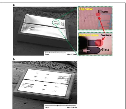
stresses of samples 2 and 3 are 1.58 MPa and 9.27 MPa, respectively, which is much lower than the maximum von Mises stress of sample 1 (89.50 MPa). For the samples, the glass pillars are arranged in the cavity. The presence of these glass pillars greatly affects the stress reduction. Figure 6 shows the SEM image and the optical micro-scope image of the fabricated samples 1 and 3. As shown in Fig. 4, sample 1 was broken during the CMP process in the region where the von Mises stress is concentrated. On the other hand, sample 3 was stably prepared for the CMP process after the anodic bonding process by
relieving the stress concentration using the glass pillars. When the von Mises stress is concentrated over 69 Mpa during the CMP process, the glass will be destroyed first (see bottom view of Fig. 6). It is believed that the sharp edges and particles of the broken glass destroyed the sili-con substrate (see top view of Fig. 6).
The simulation results show that the higher the BAR is, the lower the stress is, during the CMP process. However, if the BARs are similar as in the case of samples 1, 2, and 3, additional factors must be considered during the stress analysis. As mentioned above, sample 2 and 3 signifi-cantly reduced the stress by using glass pillars, although the BAR was similar to sample 1. In samples 2 and 3, the glass pillars supporting the cavity were arranged at inter-vals of 0.32 μm and 1.2 mm, respectively; the two samples used glass pillars with a similar BAR, but samples 2 and 3 were designed to have narrow and wide spacing arrange-ments of glass pillars, respectively. Sample 2 has under-gone the less stress, because the glass pillars of sample 2 were more densely dispersed compared to sample 3. In
Table 1 CMP process conditions of anodically bonded substrate
Temperature
(°C) P(kPa)out Pin (Pa) Silicon thickness (μm)
Glass cavity depth (μm)
Glass thickness (μm)
25 5.37 1.33 60 30 675
other words, the distribution of glass pillars apparently has a greater impact on stress distribution than the BAR, in the case of structures having a similar BAR. Table 2
shows the comparison of bonding properties for the four types of cavity pattern samples. Consequently, the anodi-cally bonded areas and distribution of the glass pillars play a major role in preventing the fracture of the anodi-cally bonded substrates during the subsequent CMP process.
Conclusion
Anodically bonded substrates having a large cavity are fabricated for a silicon MEMS device. Anodic bonded substrates with four different bonding areas are simulated for the analysis of stresses, occurring during the CMP process. In order to prevent anodically bonded substrate Fig. 5 Maximum von Mises stress for each sample
fracture, the stress intensity of four samples is analyzed according to the bonded area and pattern of the glass pil-lar arrays inside the cavity. As the ratio of bonded area to cavity area increased from 7.0 to 21.2%, the von Mises stress occurring during the CMP process was relieved from 89.5 to 0.3 MPa. As a result, the anodically bonded area and the distribution of the glass pillars inside the cavity are important factors for a stable subsequent CMP process, impacting the productivity, reliability and fabri-cation yield of the MEMS device.
Authors’ contributions
All authors read and approved the final manuscript.
Author details
1 Division of Electronics and Information Engineering, Chonbuk National Uni‑ versity, Jeonju 54896, Republic of Korea. 2 Microinfinity Co., Ltd, Suwon 16229, Republic of Korea. 3 Centre Tecnològic de Telecomunicacions de Catalunya, CERCA , Castelldefels, 08860 Barcelona, Spain. 4 Department of Electronic Engi‑ neering, Chonbuk National University, Jeonju 54896, Republic of Korea.
Acknowledgements Not applicable.
Competing interests
The authors declare that they have no competing interests.
Availability of data and materials Not applicable.
Funding
This work was financially supported by the National Research Foundation of Korea (NRF‑2017R1A2B4005687). Part of this work has been supported by the Generalitat de Catalunya under Grant 2017 SGR 891.
Publisher’s Note
Springer Nature remains neutral with regard to jurisdictional claims in pub‑ lished maps and institutional affiliations.
Received: 7 October 2018 Accepted: 4 December 2018
References
1. Cunningham Shawn, Kupnik Mario (2011) Wafer bonding. In: Ghodssi Reza, Lin Pinyen (eds) MEMS materals and processes handbook. Springer, New York
2. Hinzel DH, Goldsmith CL, Linder LF (2003) Method of integrating MEMS device with low‑resistivity silicon substrates. US Patent 6,559,530 B2, May, 2003
3. Seki T, Uno Y, Narise K, Masuda T, Inoue K, Sato S, Sato F, Imanaka K, Sugiyama S (2006) Development of a large‑force low‑loss metal‑contact RF MEMS switch. Sens Actuators A 132(2):683–688
4. Lee Byeungleul, Seok Seonho, Chun Kukjin (2003) A study on wafer level vacuum packaging for MEMS devices. J Micromech Microeng 13(5):663–669
5. Auersperg J, Auerswald E, Collet C, Dean Th, Vogel D, Winkler Th, Rzepka S (2018) Investigations of the impact of initial stresses on fracture and delamination risks of an avionics MEMS pressure sensor. Microelectron Reliab 87:238–244
6. Ma Zhibo, Wang Yinan, Shen Qiang, Zhang Han, Guo Xuetao (2018) Key processes of silicon‑on‑glass MEMS fabrication technology for gyroscope application. Sensors. 18(4):1240
7. Sim S, Lee Y, Kang H‑L, Hwang Y, Park C‑H, Llamas‑Garro I, Kim J‑M (2017) Stress analysis of anodic bonded wafer after CMP process In: Proceed‑ ings of 43rd international conference on micro and nano engineering (mne2017), 18–22 September 2017
8. Ring Terry A, Feeney Paul, Boldridge David, Kasthurirangan Jaishankar, Li Shoutian, Dirksen James A (2007) Brittle and ductile fracture mechan‑ ics analysis of surface damage caused during CMP. J Electrochem Soc 154(3):H239–H248
Table 2 Comparison of bonding properties for the cavity patterns
Sample 1 Sample 2 Sample 3 Sample 4
Area of glass pillar (mm2) 2.8 3.1 3.5 8.6
Bonding area rate (%) 7.0 7.8 8.6 21.2
Maximum von Mises stress (MPa) 89.50 1.58 9.27 0.3