IJSRSET185303 | Published : 28 April 2018 | March-April-2018 [(5) 3 : 22-31]
Themed Section : Engineering and Technology © 2018 IJSRSET | Volume 5 | Issue 3 | Print ISSN: 2395-1990 | Online ISSN: 2394-4099
22
Circuits for Digital Modulation Applications
Atul Kumar Varshney1, Vipul Sharma2
12ECE Department, Faculty of Engineering and Technology, Gurukula Kangri Viswavidhyalyaya, Haridwar
(U.K.), India
[email protected],[email protected]2
ABSTRACT
In this paper, some circuits for digital modulation applications circuits are performed using an IC and few components on project board. For generation of these circuits for digital communication modulation application experiments, various costly, heavy-weighted and tedious circuits and devices have been discovered and are available. This paper presents a very economic, light-weighted and simple circuits, those uses one or two LF 398 IC, LM 741 IC and a single resistor and/ or capacitor for generation of PAM, natural sampling, flat-top sampling, sample and hold, PAM-TDM, PWM, ASK, FSK & PSK modulation against conventional transistor based methods. Tested hardware circuits and their resultant observed waveforms have been included that justify behavior of the hardware circuitry. Laboratory implementation of digital modulation applications have been presented in this work.
Keywords: LF 398 IC, PAM, PWM, Natural Sampling, Flat-Top Sampling, Sample and Hold, PAM-TDM, ASK, FSK & PSK
I. INTRODUCTION
Analog signals, such as music, are often converted to, and stored in, digital form. To do this, the analog signal is periodically sampled (its instantaneous value is acquired by a circuit), and that constant value then hold and is converted to a digital word. For example, music signals are often sampled at 44 kHz, which means there are just a bit more than 20 microseconds available to sample, hold, and then convert the sampled value to a digital word. Then, the whole process of sample/hold/convert happens again. So, any type of analog-to-digital converter must contain, or be preceded by, a circuit which holds the voltage at the input to the ADC converter constant during the entire conversion time. Conversion times varied widely from nanoseconds (for flash ADCs) to microseconds (for successive approximation ADCs) to hundreds of milliseconds (for dual-slope integrator ADCs). In
sample and hold experiment we will use a sample and hold integrated circuit, controlled by an external clock (square wave) signal, and observe its output for a variety of input signals. In addition, the droop rate of the sample and hold IC will be measured with different values of hold capacitor.
In natural sampling and flat top sampling experiments, the properties and limitations of the sampling theorem were investigated. Specific sampling circuits have been constructed and tested using a variety of input signals and sampling signals.
In Pulse amplitude modulation (PAM) experiment amplitude of square wave pulse is varied in accordance with sinusoidal message signal. A specific PAM circuit has been constructed and tested using a variety of input message signals and square wave carrier frequencies [1, 7, 8, 9, 10, 15].
In Pulse width modulation (PWM) experiment width or duration of square wave pulse is varied in accordance with sinusoidal message signal. A specific PAM circuit has been constructed and tested using a variety of input message signals and square wave pulse frequencies [1, 7, 8, 9, 10, 15].
In pulse amplitude modulation time division multiplexing (PAM-TDM) experiment variety of input signal combinations has been chosen and tested on hardware [7, 8].
In digital communications, the modulating wave consists of stream of binary digits or an M-ary encoded version of it. High frequency sinusoidal is best choice for carrier [9]. The modulation process involves switches or keying the amplitude, frequency, or phase in accordance with the incoming binary data. The result of this modulation process is amplitude shift keying (ASK), frequency shift keying (FSK), or phase shift keying (PSK), respectively [1, 7, 9]. PSK and FSK signals are much more widely used than ASK signals in microwave radio links and satellite channels because PSK and FSK modulations have constant envelope and do not have any amplitude nonlinearity [4, 10]. Numerous costly, heavy-weighted and tedious kit based circuits and devices have been discovered and are available for generation of these digital shifts keying techniques. This paper demonstrates a very economic, portable and simplest tested circuits using a single LF 398 IC [5] and a single 39 KΩ resistor for generation of ASK and FSK modulation whereas PSK modulation also consists a LM 741 op-amp inverter [2, 3]. Tested hardware circuits and their resultant observed waveforms have been included that justify behavior of the hardware circuitry. In addition, the added advantages of this paper are lower value of dc
supply voltage and lower value of resistor that helps in lowering the cost of needed hardware circuitry.
The remaining sections of this paper describes literature review, circuit diagrams for generation of digital communication experiments, modulation techniques and their output waveforms followed by results and concluding remarks.
II. LITERATURE REVIEW
A. Sample And Hold LF 398 IC
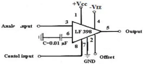
LF 398 IC is an 8-Pin IC as shown in fig.1. LF 398 is very important IC for analog and digital communication modulation generation. Its functional diagram includes a precision half wave rectifier, a comparator that compares digital data (basically a square wave) with a logic reference voltage, an n-channel FET (MPF 102) that work as a switch and a voltage follower circuit as illustrated in fig. 2. Detailed connection diagram of LF 398 IC has been shown in fig.3 [17].
B. General Description
The LF198/LF298/LF398 is a monolithic sample-and-hold circuits which utilize BI-FET technology to obtain ultra-high dc accuracy with fast acquisition of signal and low drop rate. Operating as a unity gain follower, dc gain accuracy is 0.002% typical acquisition time is as low as 6 μs to 0.01%. A bipolar input stage is used to achieve low offset voltage and wide bandwidth. Input offset adjust is accomplished with a single pin, and does not degrade input offset drift. The wide bandwidth allows the LF198 to be included inside the feedback loop of 1 MHz op-amps without having stability problems. Input impedance of 1010 Ω allows high source impedances to be used
without degrading accuracy.
temperature instabilities. The overall design guarantees no feed-through from input to output in the hold mode, even for input signals equal to the supply voltages [12].
C. Features
Some important specifications of LF 398 IC [12]: Operates from ±5V to ±18V supplies Acquisition time < 10 μs
TTL, PMOS, CMOS compatible logic input 0.5 mV typical hold step at Ch = 0.01 μF
Gain accuracy 0.002%
Low output noise in hold mode
Input characteristics do not change during hold mode
High supply rejection ratio in sample or hold Wide bandwidth
Input offset voltage 7to 10mV. Input bias current 50 to 100nA.
Input impedance very high (1010 Ω) of the
order of few GΩ.
Output impedance very low 4Ω. Logic and logic reference input current 10µA.
Leakage current into hold capacitor 200nA.
Figure1. Sample and Hold LF 398 IC
Figure 2. Functional diagram of LF 398 IC
Figure 3. Connection diagram of LF 398 IC
D. Digital Modulation Techniques
Digital modulation can easily detect and correct the noise. Information security is more in digital modulation. Digital modulated signal can travel a long distance. Because of the following advantages digital modulation schemes are most widely used in all over the world for various modes of communications [2, 3, 17]. A verity of simulated results and waveforms for digital communication laboratory have been shown using PROTES software [18].
III. GENERATION METHODOLOGY AND OBTAINED RESULTS
Very cost-effective, simplest compact circuits those utilizes one or two LF 398 IC, LM 741 IC and a single resistor and/ or capacitor methodologies for generation of PAM, natural sampling, flat-top sampling, sample and hold, PAM-TDM circuits and methodologies of generation ASK, FSK and PSK digital modulation techniques. It uses LF 398 IC, few other circuit components have been illustrated and implemented on laboratory project board in fig. 4 to fig.12, and their results obtained on CRO screen have been shown.
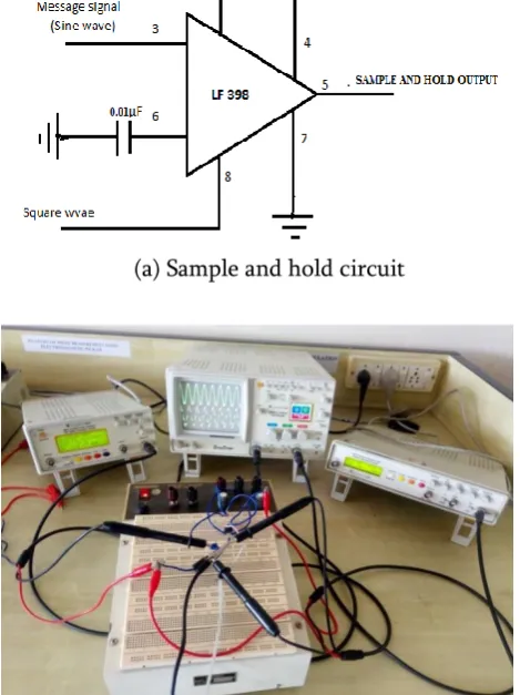
(a) Sample and hold circuit
(b) Implementation of Sample and Hold Circuit
(c) Message signal and Sample and hold output waveform
Figure 4. Generation of Sample and Hold Output Waveform
B. Generation of Pulse Amplitude Modulation (Pam) Waveform
(a) PAM Circuit
(b) Implementation of PAM
(c) Message Signal and PAM Output Waveform Figure 5. Generation of PAM Output Waveform
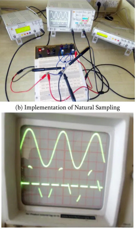
(a) Natural Sampling Circuit
(b) Implementation of Natural Sampling
(c) Message Signal and Natural Sampling Output Waveforms
Figure 6. Generation of Natural Sampling Output Waveform
D. Generation of Flat Top Sampling Waveform
(a) Flat Top Sampling Circuit
(b) Flat top sampling implementation
(c) Message signal and Flat top sampling output waveforms
Fig.7. Generation of flat top sampling waveform
(a) PAM-TDM circuit
(b) Implementation of PAM-TDM circuit
(c) Message Signal and PAM-TDM output Figure 8. Generation of PAM-TDM
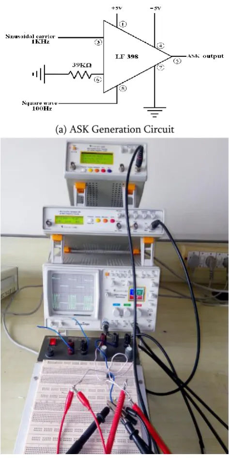
F. Generation of Amplitude Shift Keying (Ask) Waveform
ASK modulation realized using a LF 398 IC and a 39 KΩ resistor.
(a) ASK Generation Circuit
(b) Implementation Digital Data Input and ASK Output Waveform
Figure 9. ASK Waveform Generation
G. Generation of Frequency Shift Keying (FSK) Waveform
(a) FSK Generation circuit
(b) FSK Implementation and Its Output Waveform Fig. 10. FSK Waveform Generation
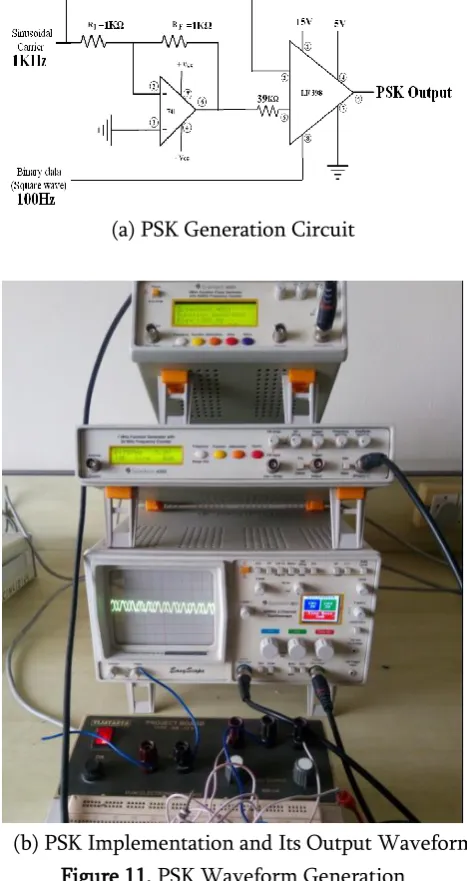
H. Phase Shift Keying (PSK)
PSK modulation realized using an op-amp 741 IC inverter followed by LF 398 IC and a 39 KΩ resistor.
(a) PSK Generation Circuit
(b) PSK Implementation and Its Output Waveform Figure 11. PSK Waveform Generation
I. Generation of Pulse Width Modulation (PWM) waveform
(b) PWM Implementation
(c) Output Waveform of PWM Figure 12. PWM Waveform Generation
IV. RESULTS
The circuit used for generation of sample and hold, PAM, natural sampling, Flat top sampling, PAM-TDM, ASK, FSK and PSK experiments had been arranged on project board. Message signals, binary inputs data and carrier waves were applied from the function generator/s, their amplitude and frequencies were adjusted suitably. Finally, the resultant output digital communication particular application wave has been obtained and observed on the cathode ray oscilloscope (CRO) as shown in fig. 4 to fig.12. Tabulated results have been shown in I to table-VII.
SAMPLE AND HOLD RESULTS S.No. Analog input message
signal (Sine Wave)
Control switching input (Square Wave)
Amp. Freq. Amp. Freq.
1 4 V(pp) 316 Hz 4 V(pp) 4.35 KHz
2 8 V(pp) 316 Hz 8 V(pp) 3.28 KHz
PAM RESULTS
S.No. Analog input
message signal
(sine wave)
Sampling
signal(square wave)
Amp. Freq. Amp. Freq.
1 4 V(pp) 316 Hz 4 V(pp) 3.27 KHz
2 8 V(pp) 316 Hz 8 V(pp) 3.28 KHz
3 8 V(pp) 316 Hz 4 V(pp) 8.09 KHz
4 8 V(pp) 316 Hz 2.5 V(pp) 8.08 KHz
NATURAL SAMPLING RESULTS
S.N o.
Analog input message signal(sine wave)
Sampling signal
frequency(square wave)
Amp. Freq. Amp. Freq.
1 8 V(pp) 318 Hz 8 V(pp) 3.01 KHz
2 8 V(pp) 316 Hz 8 V(pp) 764 Hz
3 8 V(pp) 316 Hz 8 V(pp) 7.90 KHz
4 8 V(pp) 316 Hz 8 V(pp) 30.57 KHz
5 8 V(pp) 318 Hz 8 V(pp) 1.00 KHz
FLAT TOP SAMPLING RESULT
S.No. Analog input
message signal(sine wave)
Sampling signal
frequency(square wave)
Amp. Freq. Amp. Freq.
1 8 V(pp) 318 Hz 8 V(pp) 2.65 KHz
2 8 V(pp) 225 Hz 8 V(pp) 2.65 Hz
3 8 V(pp) 225 Hz 8 V(pp) 1.91 KHz
PAM-TDM RESULTS S.N o Message 1 (sine wave) input Message 2 (triangular wave) input Sinusoidal carrier signal(square wave)
Amp. Freq. Amp. Freq. Amp. Freq. 1 4V(p
p) 415 Hz 2.4V(p p) 788
Hz 4V(pp)
3.87K Hz 2 6V(p
p) 415 Hz 2.5V(p p) 788
Hz 4V(pp)
3.87K Hz 3 8V(p
p) 415 Hz 4.2V(p p) 788
Hz 4V(pp)
3.87K Hz
Digital Modulation Techniques
Binary data (square wave) input
Sinusoidal Carrier1
Sinusoidal carrirer2
Amp. Freq. Amp. Freq. Amp. Freq. ASK
4V(pp) 100
Hz 4V(pp) 1KHz --- --- FSK
4V(pp) 100
Hz 4V(pp) 1KHz 4V(pp) 3KHz PSK
4V(pp) 100
Hz 4V(pp) 1KHz --- ---
PWM Results
S.No. Analog input message signal (sine wave)
Triangular wave
Amp. Freq. Amp. Freq.
1 4 V(pp) 50 Hz 2.3 V(pp) 600 Hz
2 6 V(pp) 82 Hz 2.1 V(pp) 1.36 KHz
3 8 V(pp) 100
Hz
2.6 V(pp) 1.36 KHz
V. CONCLUSION
The circuit used for generation of sample and hold, PAM, natural sampling, flat top sampling, PWM, PAM-TDM, ASK, FSK and PSK are arranged, realized and demonstrated using LF 398 IC and few other circuit passive components. All waveforms are observed on CRO has been justified the results. In this paper, we reduces the value of desired resistor and DC supply voltage from 15V to a pencil cell upto 5-9V, these advantages enhances a very low cost and simple circuitry based generation of digital communication laboratory experiments. Thus these circuits surely become the first choice in optical fiber and microwave link modulation schemes. These circuits are also help full for digital communications laboratory purposes for graduate and post graduate students. LF 398 IC is not limited to only these digital modulation applications but we can also generate analog modulations DSB-SC AM, FM, PM waves too. LF 398 IC could also be used to produce sample and hold circuit for reconstruction of sampling and natural sampling, and flat-top sampling in conjunctions with few filter circuits and other simple ICs. Pulse amplitude modulation and Time Division Multiplexing circuits have been also be implemented and verified those omits the use of very
costly kits available in the laboratory. So we conclude that by the use of LF 398 IC, we can replace our communication laboratory economic and hands-on rather than using costly kits.
VI. REFERENCES
[1] S. Haykin, “Digital Communications”, reprint, John Wiley & Sons, 2001.
[2] B. Kamini, “An alternate approach to the lboratory implementation of communication experiments”, Digital signal processing education workshop & IEEE, 2011.
[3] A. Goyel, “ Generation of ASK, FSK & PSK using sample and hold IC LF 398”, in Proc IEEE xplore, International conference on signal processing & communication (ICSC), Delhi, 2016, pp. 51-54.
[4] J. Milliman and C. C. Halkias, “Integrated Electronics,” 2 ed., Tata McGraw Hill, 1991. [5] D. R. Choudhury & S. B. Jain, “ Linear
Integrated Circuits”, 4 ed., New Age International Publication, 2012.
[6] J. G. Prokis, “ Digital Communications”, 4 ed., McGraw Hill, 2000.
[7] B. P. Lathi, “ Modern Digital and Analog Communication systems”, 3ed., Oxford University Press, 1998.
[8] A. B. Carlson and P. B. Crilly, “Communication Systems”, McGraw Hill, 5 ed., 2010.
[9] W. Tomasi, “Electronics Communication Systems Fundamentals Through Advanced”, 5 ed., Printice Hall India, 2008.
[10] A. K. Varshney,“Digital and Analog Communication”, 1 ed., International Book House publication, 2011.
[11] I. Xilinx, “Design Suit”, 2012.
[12] National Semiconductors, LF 398 data sheet. [13] National Semiconductors, LM 741 data sheet. [14] A. Sharma, S. Majumdar and A. Naugarhiya,
[15] S. Haykin, “Communicztion Systems”, 2 ed.”, Wiley Estern Limited, 1983.
[16] G. Kennedy, “Electronic Communication Systems”, 3 ed., Tata McGraw Hill, 1989. [17] A. Varshney, “A Cost Effective Generation of
Digital Modulation Techniques(ASK, FSK & PSK) Using LF 398 IC”, Recent trends in analog devices and circuits, vol. 1, issue 1, HBRP, 2018.
[18] B Kanmani, “Digital Communication Using Labview”, MITE-2013, IEEE International Conference on MOOC, Innovation and Technology in Education (MITE), Jaipur, 20-22 December, 2013.