On Chip Calibration For A 7 Bit Comparator
Based Asyncronous Binary Search (CABS) A/D
Converter
Vikash Kumar Singh, Kumari Archana
Abstract: An on-chip calibration technique has been proposed for a 7-bit Comparator Based Asynchronous Binary Search (CABS) A/D Converter. The proposed design is veri-fied using an 8-bit, 3.3V, 10 MS/s Asynchronous SAR A/D Converter by integrating the calibration scheme into the A/D Converter. The 8-bit Asynchronous SAR A/D Converter consists of a track-and-hold followed by a two-step conversion process. The two-step architecture consists of a 1-bit course and a 7-bit fine converter. The 1-bit coarse converter is implemented using the SAR-CC principle and the 7-bit fine converter is implemented using the CABS principle. The 7-bit CABS sub-A/D converter consists of 127 comparators with differ-ent threshold voltages. All these 127 comparators with different threshold voltages are calibrated using a calibration technique in which the thresholds are adjusted to the desired value by tuning the total current flowing through the differential pair in the comparator circuit. The calibration technique and the A/D converter have been designed in 0.18 mm CMOS technology with a supply voltage of 3.3 V. The simulation results showed an ENOB of 6.7 for SNDR of 42.09 dB at Nyquist frequency.
Index Terms: 2-step 8-bit ADC Architecture, Calibration of 7-bit CABS ADC, 7-bit CABS stage
————————————————————
1
I
NTRODUCTIONAs data conversion interfaces are designed for higher preci-sions, the non-idealities that accompany monolithic device such as mismatch, non-linearity and finite intrinsic gain of a transistor, limits the raw resolution to approximately 6 bits in CMOS technology. For higher resolutions, it is often necessary to correct for these effects in the design phase itself by means of a circuit or algorithmic techniques. Such techniques are ap-plied to individual building blocks to improve their precision, as well as to the overall architecture to make its output characte-ristics approach the ideal. In addition to the reg-ular mode of operation, circuits employing some of these techniques typical-ly require a dedicated period to carry out calibration, thereby complicating the system‘s timing schedule. This project aims at designing an on-chip calibration technique for a 7-bit Com-parator Based Asynchronous Binary Search (CABS) A/D Con-verter. The proposed calibration setup adjusts the threshold voltages to the desired values by tuning the total current flow-ing through differential pair, thereby reducflow-ing the effect of mismatch and process variation. Hence the overall accuracy of the ADC is improved by using cali-bration. The data conver-sion rate of 10 Mega-Samples Per Second (MS/s) is targeted in this design. Transistor level circuits are designed using 0.18 mm CMOS technology. The circuit design and transient simu-lations are done in LTspice. The simulation data is exported to MATLAB for frequency domain analysis in order to measure the dynamic performance metrics of the ADC.
2
A
NALOG TOD
IGITALC
ONVERSIONAnalog to Digital Conversion is an essential function in data processing systems. A/D Converters (ADCs) interface the digi-tal signal processors with the analog world input. This chapter discusses the basic concepts and operations related to A/D conversion followed by the definition of various static and dy-namic performance metrics.
2.1 Basic Conversion Principle
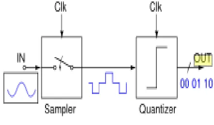
Analog-to-digital conversion consists two distinct operations: sampling and quantiza-tion. Sampling converts a continuous time, continuous amplitude analog signal into a discrete time, continuous amplitude signal, while quantization converts the continuous amplitude of this sampled signal into a set of dis-crete levels. Figure 2.1 shows the principle of A/D conversion.
Figure 2.1: Principle of A/D conversion
The I/O characteristics of an ideal 3-bit ADC is shown in Fig-ure 2.2
————————————————
Vikash Kumar Singh is currently pursuing Masters De-gree program in Embedded System and VLSI Designf rom LIET, JNTU Hyderabad.
E-mail: [email protected]
PH: +91-9000764778
Kumari Archana is currently pursuing Master’s degree program in Embedded System and VLSI Designfrom LIET, JNTU Hyderabad.
11
Figure 2.2: Input/output characteristic of 3-bit ADC.
3. 2-step, 8-bit ADC Architecture 3.1 ADC Specifications
The following are the design specifications of the A/D conver-ter.
Supply voltage 3.3 V
Reference voltage 1 V
Architecture 2 step fully differential
Maximum differential input 2 V (peak to peak)
Input common mode 1.65 V
Frequency of operation 10 MS/s
Resolution 8 bits
Technology 0.18 mm CMOS process
3.2 Two step ADC architecture
The 2-step architecture proposed in has been modified for 8-bits and the block dia-gram of 2-step, 8-bit Architecture is shown in Figure 3.1. The 8-bit A/D Converter is implemented using a sample & hold circuit followed by a 2-step conversion pro-cess. The 2-step architecture consists of a 1-bit course and 7-bit fine converter. The 1-bit coarse converter is imple-mented using the SAR-CC principle and the 7-bit fine conver-ter is implemented using the CABS principle.
Figure 3.1: 2-step, 8-bit Architecture
Digital output of this 2-step, 8-bit Architecture will be in signed 2‘s complement form.
• 1-bit SAR gives the sign bit.
• 7-bit CABS stage gives the magnitude bits.
3.2.1 Operation of SAR-CC
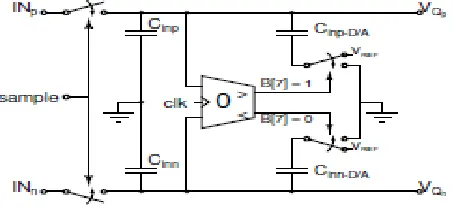
The circuit diagram of 1-bit SAR-CC sub A/D converter is shown in Figure 3.2.
Figure 3.2 SAR-CC sub A/D Convertrer
Initially both the capacitors (i.e, Cinp�D=A & Cinn�D=A) are connected to VREF. Depending on the output of the compara-tor, one of the capacitor is disconnected from VREF and grounded, in this way subtracting charge on either the positive or negative node. This operation changes both the differential and the common mode signal levels. The operation of SAR-CC can be analyzed mathematically as follows. Let us assume that INp > Inn. Total charge on the node VQp before the com-parator makes decision is given by
Total charge on the node VQp after the comparator makes decision is given by
By the law of conservation of charges equating Q1 and Q2
if Cinpdtoa = Cinp, then eq 3.3 reduces to
Total charge on the node VQn after the comparator makes decision is given b
By the law of con-servation of charges equating Q3 and Q4
Similarly for INp < INn, it can be shown that
From equations 3.4, 3.7, 3.8 & 3.9 it is clear that once the 1-bit converter makes a decision, it subtracts a charge which cor-responds to VREF2 either from the node VQp or from the node the VQn depending on whether INp > INn or INp < INn. This operation brings the differential signal into the input range of the 7-bit CABS A/D Converter.
3.2.2OPERATION OF CABS SCHEME
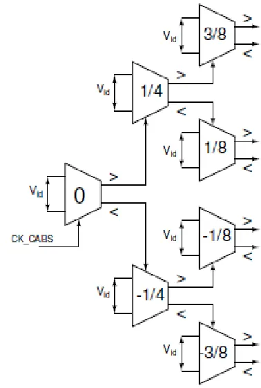
The operating principle of the CABS converter is based on Asynchronous binary search, the same principle that is used in a successive approximation A/D Converter. But in the CABS architecture instead of approximating the input signal, the comparators with built-in thresholds are used to bracket the input signal. Figure 3.3 shows the CABS architecture instead of approximating the input signal; the comparators with built-in thresholds are used to bracket the input signal. Figure 3.3 shows the CABS architecture illustrated for 3-bits, but it can be extended to more number of bits.
Figure 3.3: CABS A/D converter, shown for 3-bits
Similar to a flash converter, the sampled input signal is applied to all comparators, but all the comparators are not clocked (like in a Flash ADC). Instead the comparators are connected in a binary tree, in which the root comparator compares the input signal with zero and based on its decision synchronously triggers one of the comparator in the next level, (i.e, compara-tors with threshold 1/4 and -1/4). If the input signal is greater than zero the comparator with threshold 1/4 is triggered, if smaller than zero, the comparator with threshold -1/4 is trig-gered. This second comparator in turn triggers one of the comparators in the third layer, thereby closing in on the input signal. Based on the outputs of the activated comparators an unsigned binary code is derived: logic 1 is encoded for Input greater than threshold and logic 0 for Input lesser than thre-shold.
3.2.3 DESIGN OF COMPARATOR CIRCUIT WITH EMBEDDED THRESHOLD
An N-bit CABS stage requires ‗2N�1‘ comparators with differ-ent built-in threshold voltages. The 3-bit CABS circuit contains 7 comparators each with different built-in threshold voltages. So, the 7-bit CABS stage rquires 127 comparators with differ-ent built-in threshold voltages. In order to achieve this it is ne-cessary to know, upon which parameters the comparator thre-shold depends.
Threshold voltage of an NMOS differential pair
13
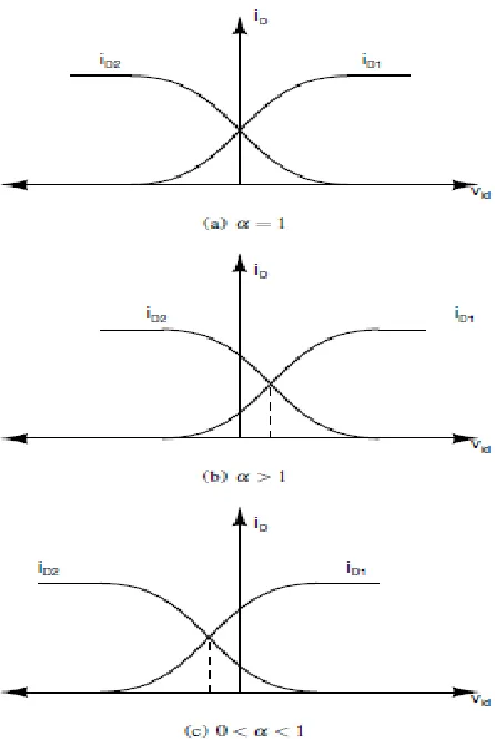
Fiure 3.4: Differential pair with different (W/L) ratios From the Figure 3.4 Vid can be written as
If M1 and M2 are in saturation, then
Solving the equations 3.10 & 3.11 for iD1 & iD2, we get
Now we can obtain the threshold by finding vid at which iD1-iD2 = 0. Therefore by solving iD1�iD1-iD2 = 0 for Vid, we get
The variation of threshold voltage for different values of ‗a‘ is shown in Figure 3.5. From the equation 3.14, it is clear that the threshold voltage can be controlled by I tail and a (i.e, ratio ofW/L)s of M1 and M2 transistors of NMOS differential pair shown in Figure 3.4). So, comparator circuits with different threshold voltages are designed using a differential pair by properly choosing Itail and values.
Figure 3.5: Threshold variation of a comparator
Comparator circuit and its operation
Basically a comparator consists of three components. They are
• Current mirroring circuit (M3 through M6) • PMOS differential pair (M1 and M2) • latch circuit (M7 through M10)
This comparator circuit operates in two phases. They are
• Reset Phase (i.e, when Comp signal is at logic ‗0‘): In this phase, all the internal nodes of latch are grounded by using M11 through M14 transistors and the mirroring circuit is turned OFF by using M4 and M6. In this phase, both the outputs (Greater & Lesser) will be at logic ‗0‘.
• Comparison Phase (i.e, when Comp signal is at logic ‗1‘): In this phase, the applied differential input to the differential pair is compared with the threshold voltage and based on the comparison, one of the output‘s of the comparator goes to logic ‗1‘ and the other goes to logic ‗0‘ i.e, if the differential input is greater than the threshold voltage of the comparator then ‗Greater‘ signal becomes logic‗1‘ and ‗Lesser‘ signal becomes logic‗0‘and vice-versa.
4.
C
ALIBRATION OF7-
BITCABS
ADC
4.1NEED FOR CALIBRATION
Once the ADC is fabricated, due to process variations, there will be transistor mismatches. So, the transistor mismatches introduce non-linearity in the current mirroring circuit. Because of the transistor mismatches and the non-linearity in the cur-rent mirroring circuit, the threshold voltage of the comparator deviates from the desired value. Hence, non-linearity is intro-duced in the overall ADC design. So, it is necessary to cali-brate the comparators so that the effect of process variation is minimized.
4.2
C
ALIBRATION OF AN INDIVIDUAL COMPARATORThreshold voltage for an NMOS differential pair having widths is proportional to (W/L) and (W/L) asshown in Figure 4.1 is given by
Figure 4.1: Differential pair
So, it is clear that the threshold voltage of a comparator can be adjusted by varying the ‗Itail‘ and/or ‗a‘ (i.e, the ratio of (W/L)s of the differential pair). So, in this project calibration is done by
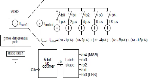
tuning the tail current. In the proposed calibration scheme ‗Itotal‘ is implemented as shown in Figure 4.2. During the cali-bration mode, the desired value of threshold has to be applied as input to the corresponding comparator. A 5-bit counter is used to tune the current to the desired value. The output of the counter is connected to binary weighted current sources hav-ing an LSB of 1mA. Since a 5-bit counter is used, the available range for tuning is 32mA with a step size of 1mA.
Figure 4.2: Implementation of ‗Itotal‘
4.2.1 CALIBRATION SETUP FOR A POSITIVE THRESHOLD VOLTAGE COMPARATOR
For a positive threshold voltage comparator, ‗Iinitial‘ is set such that
Here the 5-bit counter acts a down counter. So, the initial value of the counter is all 1‘s, which means all the binary eighted current sources are turned ON thereby setting ‗Itotal‘ greater than the desired one. This implies that the threshold has been set to a value greater than the desired value. So the ‗Lesser‘ and ‗Greater‘ output‘s of the comparator will be logic ‗high‘ and logic ‗low‘ respectively. The counter is decremented by one for every clock cycle and based on the counter code a finite even number of fingers (each pair of fingers carrying a current of 1mA) gets turned ON. Initially Itotal has been set to a value greater than the desired value. For every clock cycle Itotal is decremented by 1mA. After some clock cycles, when the ‗Itot-al‘ reaches the desired value, the output flips i.e, ‗Greater‘ be-comes logic ‗high‘ and ‗Lesser‗ bebe-comes logic ‗low‘, then the latch gets disabled thereby holding the counter code for which the outputs have flipped and thus completing the calibration process. Figure 4.3 shows the circuit diagram of the compara-tor circuit having positive threshold voltage with the calibration setup included. Here the comparator has two modes of opera-tion i.e, calibraopera-tion mode and normal mode. In the calibraopera-tion mode (i.e, when ‗calib‘ signal becomes logic ‗1‘),
• Desired threshold voltage is applied across the PMOS differential pair and it is held till the calibration of the comparator is complete.
• Depending on the counter code a finite number of fin-gers is turned ON.
15
on a finite number of fingers in the current mirroring circuit. The comparator makes a
• decision based on the comparison for every clock cycle.
• Once the desired threshold is set, the latch gets dis-abled and the counter value is held and thus fixing the number of fingers to be connected in the current mir-roring circuit. This completes the calibration phase for that comparator.
• Since the initial state of latches is not known, latch output nodes are groundedusing M30 through M34 transistors.
• M25 through M29 transistors are used to turn ON all the fingers initially.
In the normal mode (i.e, when ‗calib‘ signal becomes logic ‗0‘),
• For each clock cycle, the comparator compares the differen-tial input signal applied across the PMOS differendifferen-tial pair with the it‘s threshold voltage. The comparator makes a decision based on the comparison for every clock cycle.
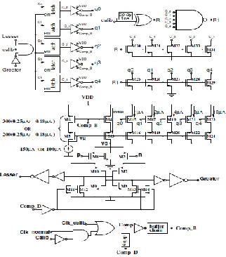
Figure 4.3: Circuit diagram of a positive threshold voltage comparator
4.2.2CALIBRATION SETUP FOR A NEGATIVE THRESHOLD VOLTAGE COMPARATOR
For a negative threshold voltage comparator ‗Iinitial‘ is set such that
Here the 5-bit counter acts a up counter. So, the initial value of the counter is all 0‘s, which means all the binary weighted
cur-rent sources are turned OFF thereby setting ‗Itotal‘ lesser than the desired one. This implies that the threshold has been set to a value lesser than the desired value. So the ‗Lesser‘ and ‗Greater‘ output‘s of the comparator will be logic ‗low‘ and logic ‗high‘ respectively. The counter is incremented by one for every clock cycle and based on the counter code a finite even number of fingers (each pair of fingers carrying a current of 1mA) gets turned ON. Initially Itotal has been set to a value
lesser than the desired value. For every clock cycle Itotal is incremented by 1mA. After some clock cycles, when the ‗Itotal‘ reaches the desired value, the output flips i.e, ‗Greater‘ be-comes logic ‗low‘ and ‗Lesser‗ bebe-comes logic ‗high‘, then the latch gets disabled thereby holding the counter code for which the outputs have flipped and thus completing the calibration process. In the calibration mode (i.e, when ‗calib‘ signal be-comes logic ‗1‘),
• Desired threshold voltage is applied across the PMOS differential pair and it is held till the calibration of the comparator is complete.
• Depending on the counter code a finite number of fin-gers is turned ON.
• For each clock cycle, the comparator compares the applied differential input (Desired threshold voltage) with the present threshold voltage i.e, set by turning on a finite number of fingers in the current mirroring circuit. The comparator makes a
• decision based on the comparison for every clock cycle.
• Once the desired threshold is set, the latch gets dis-abled and the counter value is held and thus fixing the number of fingers to be connected in the current mir-roring circuit. This completes the calibration phase for that comparator.
• Since the initial state of latches is not known, latch output nodes are grounded using M25 through M29 transistors.
In the normal mode (i.e, when ‗calib‘ signal becomes logic ‗0‘),
• For each clock cycle, the comparator compares the differential input signal applied across the PMOS dif-ferential pair with the it‘s threshold voltage. The com-parator makes a decision based on the comparison for every clock cycle.
4.3 CALIBRATION SETUP FOR THE 7-BIT CABS A/D
CONVERTER
This calibration scheme employs only one 5-bit up/down coun-ter to calibrate all the 127 comparators of the CABS. So, only one comparator can be calibrated at a time. This project re-quires calibration of 127 comparators one after the other. So to select one comparator out of 127 comparators for calibration, a 1x128 Demux is used. Here, the comparators are calibrated in a particular order (i.e, level by level starting from MSB to LSB) so that an error in one level due to threshold variation, is not carried to the next level.
Figure 4.4: Calibration set up for the entire ADC
The output pins of the Demux should be connected to
compa-rators in such a way that they are calibrated level by level. A 7-bit up-counter is used to generate selection lines for Demux and the same counter codes are applied as input to ideal 7-bit DAC, so as to generate the required input threshold voltages during calibration. Since a 5-bit up/down counter is used for calibration, a maximum of 32 clock cycles are required for ca-librating each comparator. DAC generates a differential Analog voltage corresponding to that code and is applied to all the comparators. At the same time 1x128 Demux selects one of the 127 comparators for calibration and the Clock signal is applied to that comparator only. Based on the LSB of 7-bit up counter, the operation of 5-bit counter (i.e, whether it should act as up/down counter) is decided. 5-bit counter incre-ments/decrements for each clock cycle. After 32 clock cycles, the 7-bit up counter code is incremented by 1 and the 5-bit counter is cleared. Now the new 7-bit up counter code is ap-plied as input to ideal DAC and 1x128 Demux and the process continues until all the comparators are calibrated
.
The flow-chart for the calibration process is shown in the Figure 4.5Figure 4.5: flowchart for the calibration process Clock signal for 7-bit up counter and clear signal for 5-bit up/down counter has been generated as shown in Figure 4.9. The reference threshold voltages required generated by DAC during calibration has to be applied from the front end of the ADC i.e, it has to be applied to the bit SAR stage. But the 1-bit SAR subtracts Vref 2 from the applied input. To avoid this, the first stage (1-bit SAR) has to be by-passed during calibra-tion phase. This is achieved by adding some addicalibra-tional circuit as shown in the Figure 4.6 with dotted lines.
17
5.
R
ESULTS5.1TIME-DOMAIN ANALYSIS
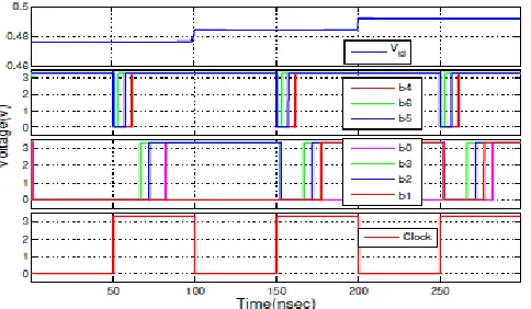
5.1.1CALIBRATION PHASE
The designed ADC is operated in calibration phase (i.e, by setting ‗calib‘ signal to logic ‗1‘). The calibration phase of com-parators with threshold voltages (32/128)V and -(32/128)V are shown in Figure 5.1 & 5.2. As mentioned earlier, the desired threshold voltage is applied as input to the comparator in the calibration phase. The desired threshold voltages has been generated using an ideal DAC and applied to the comparator during calibration phase.
Figure 5.1: Calibration phase of (32/128) V threshold voltage Comparator
Figure 5.2: Calibration phase of -(32/128) V threshold voltage Comparator
Figure 5.3 shows the calibration phases of comparators with threshold voltages (32/128)v, -(32/128)v, (16/128)v, -(48/128)v and (48/128)v. here calibration is performed level by level. (32/128)v and -(32/128)v threshold voltage comparators be-long to first level and the remaining bebe-long to second level.
Figure 5.3: Calibration phases of 1st and 2nd level Comparators
5.1.27-BIT CABS STAGE
The 7-bit CABS ADC is applied with a differential inputs of (61/128)V, (62/128)V and (63/128)V respectively with a DC common mode voltage of 1.4V as shown in the Table 5.1. A clock signal of 10MHz frequency, having a duty cycle of 50% is used foroperating the ADC.
Figure 5.4: Simulation result of CABS stage
5.2FREQUENCY-DOMAIN ANALYSIS
5.2.1THE COMPLETE ADCSYSTEM
A 100 KHz sinusoidal input of amplitude 1.0 V and DC level 1.65V (amplitude varies between 0.65 to 2.65 V) is applied to the de-signed 2-step, 8-bit ADC and the digital code generated by ADC is applied to an ideal DAC (Spice code taken from) and the simulation data is exported to MATLAB. Figure 5.5 shows the input of an ADC and the output of DAC with both DC levels adjusted to 0V and Fig-ure 5.6 shows the power spectrum of input of an ADC and the out-put of DAC.
Figure 5.5: Response of 8-bit ADC for Sinusoidal input of 100 KHz
Figure 5.6: Power Spectrum of 8-bit ADC for Sinusoidal input of 100 KHz
5.3PERFORMANCE METRICS
The performance specifications are measured from multiple transient simulations and the calculated average values are listed in the Table 5.2. The offset error and gain error shown in the table are normalized w.r.t LSB.
6
CONCLUSION
An on-chip calibration technique has been designed for a 7-bit Comparator based Asynchronous Binary Search (CABS) ADC. The on-chip calibration has been verified by using the 7-bit CABS ADC as a second stage in an 8-bit, 10 MS/s Asynchronous SAR ADC. The calibration phases of each comparator in the 7-bit ADC have been thoroughly verified. The 7-bit CABS ADC takes 4224 clock cycles for the entire calibration process In the proposed calibration technique, each comparator is alloted a fixed amount of time (33 clock cycles) for calibration. This can be reduced by selecting the next comparator (which is to be calibrated) once the desired thre-shold voltage is set for the comparator (which is being calibrated). The overall calibration time for the 7-bit ADC can also be reduced by using a higher frequency (twice) clock signal, for calibration. However the overall ruggedness of the calibration technique can only be verified after fabricating the IC.
R
EFERENCES[1] M.Waltari and K. Halonen, Circuit techniques for low-voltage and high-speed A/D converters. Springer, 2002, vol. 709.
[2] G. Van der Plas and B. Verbruggen, ―A 150MS/s 133mW 7b ADC in 90nm digital CMOS Using a Comparator-Based Asynchronous Binary-Search sub-ADC,‖ in Solid-State Circuits Conference, 2008. ISSCC 2008. Digest of Tech-nical Papers. IEEE International. IEEE, 2008, pp. 2631– 2640.
[3] M. Mano and M. Ciletti, Digital design, 1984.
[4] G. Yeap, Practical low power digital VLSI design. Springer, 1998.
[5] J. Rabaey, A. Chandrakasan, and B. Nikolic, Digital inte-grated circuits. Prentice-Hall, 1996.