A VLSI Architecture for Neural Network Chips
M a r le y M a r ia B ern a rd es R e b u z z i V ella sco
a thesis subm itted fo r the degree o f
Doctor of Philosophy in C om p u ter Science
U n iversity o f L o n d o n
D epartm ent o f C om puter Science
University College London
Gower Street, London WC1E 6BT
ProQuest Number: 10610866
All rights reserved
INFORMATION TO ALL USERS
The qu ality of this repro d u ctio n is d e p e n d e n t upon the q u ality of the copy subm itted.
In the unlikely e v e n t that the a u th o r did not send a c o m p le te m anuscript and there are missing pages, these will be note d . Also, if m aterial had to be rem oved,
a n o te will in d ica te the deletion.
uest
ProQuest 10610866
Published by ProQuest LLC(2017). C op yrig ht of the Dissertation is held by the Author.
All rights reserved.
This work is protected against unauthorized copying under Title 17, United States C o d e M icroform Edition © ProQuest LLC.
ProQuest LLC.
789 East Eisenhower Parkway P.O. Box 1346
Abstract
This thesis reports the research for the development of a neural network VLSI design environment where a neural application defined in a high-level programming environment is automatically mapped into custom VLSI chips.
This work forms the basis of the UCL hardware investigations in the Esprit II Pygmalion project into VLSI architectures for neural network chips. The ultimate goal is to take a neural network application defined by Pygmalion's neural specification language, and automatically translate it to one or more CMOS integrated circuits.
The thesis is composed of four parts: the neural network specification language; the target architecture, formed by the generic neuron model and its corresponding VLSI architecture; a simulator for the architecture; and finally a prototype Back Propagation VLSI chip.
The neural network specification language at the centre o f Pygmalion has been designed to achieve flexibility and portability to allow an easy translation from a neural network specification to either binary code, for simulation, or to silicon, for execution. The language, named nC, has been defined as a subset of C. The basic concepts and the issues concerning how to use nC are fully examined in this thesis.
The target architecture is the critical issue for automatically translating a high-level specification of a neural network into application-specific chips. Consequently, the
definition of a generic neuron model incorporating the main features o f neural
algorithms, and its associated VLSI architecture, form the main scope o f this thesis. The architecture’s communication strategy and the internal organisation o f the processing element are thoroughly investigated.
The adequacy of the proposed architectural model is analysed using a simulator implemented in the C language. Simulation results of the Back Propagation execution are presented, verifying the effects of the hardware implementation on the neural network execution.
The viability in terms of layout design has been evaluated by designing and fabricating a hand-crafted prototype VLSI chip, performing the "Back Propagation" algorithm. A detailed examination of the layout results is provided, including a full description o f the cell library designed.
Acknowledgements
I would like to acknowledge my indebtedness to my supervisor Prof. Philip Treleaven who assisted, advised and gave me tremendous support throughout this work. His guidance and continuous encouragement made the conclusion o f this thesis possible.
I am also indebted to many other staff and colleagues in the Department of Computer Science at UCL, for their valuable discussions, encouragement and friendship. In particular, I would like to thank Marco Pacheco, Carlo de Oliveira and Meyer Nigri for their irreplaceable friendship and invaluable discussions through the whole process o f the architecture specification and implementation. I am also very grateful to Michael Recce for his patience and real incentive during the writing up phase of this thesis.
I would also like to thank Dr. Peter Rounce and Dr. Apostolos Refenes for reading this report and giving invaluable comments.
Special thanks must go to all my friends, Debinha, Id ea, Cristina, Sergio, Marquinhos and many others, for their support, encouragement and friendship throughout these years.
I wish to thank the Brazilian institution CNPq and the Pontiffcia Universidade Catdlica do Rio de Janeiro for sponsoring my postgraduate studies here at University College London. In addition, I want to thank the Esprit II Galatea project for financing the fabrication of the prototype integrated circuit.
Table of Contents
C H A P T E R 1 - I n tr o d u c tio n ... 11
1.1. Neural C o m p u tin g ... 11
1.1.1. Artificial Neural N etw orks... 13
1.2. Motivations & Design Issues ... 17
1.3. Thesis G o a ls ... 19
1.4. Thesis Contributions ... 20
1.5. Thesis Organisation ... 21
C H A P T E R 2 - V L S I A rc h ite c tu r e s fo r A rtific ia l N e u r a l N e t w o r k s 23 2.1. Neurocomputers ... 23
2.1.1. Special-Purpose Neurocomputers ... 24
2.1.2. General-Purpose N eurocom puters... 33
2.2. W eight-based A rchitectures... 40
2.2.1. Siemens A rch itectu re... 40
2.2.2. Philips A rchitecture... 43
2.3. Neuron-based Architectures ... 46
2.3.1. INPG Architecture ... 46
2.3.2. UCL Architecture ... 49
2.4. S u m m ary... 52
C H A P T E R 3 - Pygm alion N e u ra l P r o g ra m m in g E n v ir o n m e n t ... 54
3.1. Neural Programming Environments ... 54
3.2. Pygmalion Programming Environment ... 57
3.3. Neural Network Representations in Pygmalion ... 61
3.3.1. N High Level L an g u a g e... 62
3.3.2. nC Specification Language ... 63
3.4. Neural Network Execution M eth o d s... 64
3.4.1. S im u latio n ... 64
3.4.2. Silicon Execution ... 65
3.5. S u m m ary ... 66
C H A P T E R 4 - nC N e u ra l N e tw o rk S p e c ific a tio n L a n g u a g e ... 67
4.2. nC Basic Concepts ... 69
4.2.1. Rule Concept ... 69
4.2.2. Generic Hierarchical Structure - system ... 72
4.2.3. nC Parallel Execution Operator - PAR ... 76
4.3. Programming an Application ... 76
4.3.1. Application Configuration Definition ... 76
4.3.2. Application Control D e fin itio n ... 78
4.4. Programming an A lg o rith m ... 79
4.4.1. Coding connect and build-rules ... 79
4.5. tiC Parser ... 80
4.6. S u m m ary... 81
C H A P T E R 5 - G eneric N euron A rch itectu re & Silicon C om pilation ... 83
5.1. Design Approach ... 83
5.2. Generic Neuron Description ... 84
5.3. Architectural F ram ew o rk ... 88
5.3.1. Communication S trateg y ... 88
5.3.2. Processing Element Overview ... 93
5.4. Processing Element Framework Implementation ... 96
5.4.1. Memory Unit ... 97
5.4.2. Communication Unit ... 100
5.4.3. Execution Unit ... 105
5.5. Silicon Compiler Parameters ... 108
5.6. S u m m ary... 110
C H A P T E R 6 - A r c h ite c tu r e S im u la tio n ... I l l 6.1. Simulator F ram ew o rk ... I l l 6.1.1. User Configuration P aram eters... 114
6.1.2. Data Structure Organisation ... 114
6.2. Back Propagation Simulation Results ... 116
6.2.1. Threshold Function Investigations... 116
6.2.2. Fixed-Point Arithmetic A n a ly sis... 118
6.2.3. Network Performance Examination ... 119
6.3. S u m m ary... 122
C H A P T E R 7 - V L S I A r c h ite c tu r a l I m p le m e n ta tio n ... 123
7.1. VLSI Design A p p ro a c h ... 123
7.2.1. Design Philosophy... 127
7.2.2. Modular Register Building Blocks ... 130
7.2.3. Functional Elem ents... 132
7.2.4. Interface and Switching Elements ... 135
7.3. Chip Organisation ... 136
7.3.1. Operative Part Organisation ... 136
7.3.2. Control Part Organisation... 138
7.4. Implementation Considerations and Results... 140
7.5. Summary... 142
C H A PTER 8 - A sse s sm e n t... 144
8.1. Target Review ... 144
8.2. nC Neural Network Specification Language ... 145
8.3. Generic Neuron Model & VLSI Architecture ... 147
8.3.1. Interconnection Schem e... 148
8.3.2. Processing Element D esign ... 150
8.4. Architecture Simulator... 152
8.5. VLSI Prototype Implementation ... 154
C H A PTER 9 - C onclusions & Future W o r k ... 158
9.1. Summary... 158
9.2. Research Contributions... 160
9.3. Future W ork... 161
REFERENCES... 164
A ppendix 1 -
nC
L anguage Syntax ... 174A ppendix 2 - D atapath Cell L ib r a r y ... 182
A ppendix 3 - Back Propagation Prototype Schem atics ... 191
List of Figures
Figure 1.1: Multilayer Neural Network... 14
Figure 1.2: Internal structure of the generic neuron model... 15
Figure 1.3: Neural Network Threshold Functions... 16
Figure 2.1: General View of a Special-Purpose Neurocomputer... 25
Figure 2.2: Personnaz & Weinfcld’s interconnection strategy... 30
Figure 23 : The Fujitsu Basic Architecture... 30
Figure 2.4: System configuration for the NTT AAP-2 architecture... 36
Figure 2.5: Adaptive Solution processor array system architecture... 38
Figure 2.6: Hitachi’s WSI neural network architecture... 39
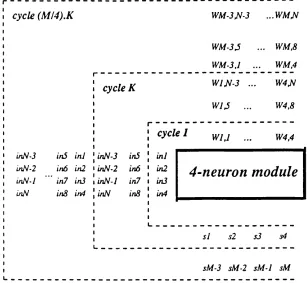
Figure 2.7: Schema of the Siemens 4-neuron module with 16 multipliers... 41
Figure 2.8: Data (low through a 4-neuron unit... 42
Figure 2.9: Philips’ basic circuit architecture... 44
Figure 2.10: INPG’s basic neural processor structure... 47
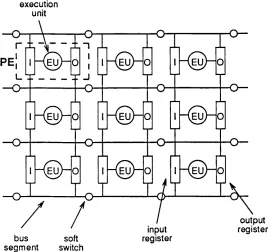
Figure 2.11: A partial view of the 2-D array of neural processors... 48
Figure 2.12: 4x2 array of neural processors... 48
Figure 2.13: Generic Neuron Architectural Framework... 50
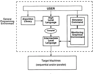
Figure 3.1: A Typical General-Purpose Programming Environment... 57
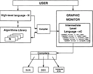
Figure 3.2: Structure of the Pygmalion Neural Programming Environment... 58
Figure 3.3: Programming a Neural Network Application... 61
Figure 4.1: Representation of the nC Programming method... 68
Figure 4.2: The Back Propagation state update of a neuron-level rule level... 71
Figure 4.3: The Back Propagation state update of a cluster-level meta-rule level... 71
Figure 4.4: The nC hierarchical structure system... 72
Figure 4.5: The complete system structure definition... 74
Figure 4.6: config general framework... 77
Figure 5.1: The structure of the generic neuron model... 85
Figure 5.2: The generic neuron's bus interconnection strategy... 90
Figure 5.3: The architecture’s interconnection strategy... 92
Figure 5.4: The multi-bus interconnection strategy... 93
Figure 5.5: The processing element’s internal structure... 94
Figure 5.6: The processing element’s internal organisation... 97
Figure 5.8: The communication unit’s internal structure... 102
Figure 5.9: Execution Unit’s internal structure... 105
Figure 6.1: Results from the investigation of the look-up table effects... 117
Figure 6.2: Results from the network performance examination... 121
Figure 7.1: VLSI Design Environment... 126
Figure 7.2: The Interconnection Structure of Cells... 129
Figure 7.3: Schematic of the basic register... 131
Figure 7.4: Carry chain circuit for the ALU... 134
Figure 7.5: Organisation of the generic neuron Operative Part... 137
Figure 7.6: Organisation of generic neuron Control Part... 139
Figure 7.7: Clock system used in the generic neuron prototype... 139
Figure 7.8: Floor Plan of the Back Propagation Prototype... 141
Figure 7.9: Back Propagation Prototype Layout ... 143
List of Tables
Table 3.1: Neural Network Programming Environments... 56
Table 5.1: The mapping of popular neural models into the generic neuron model... 86
Table 5.2: Command lines in the control bus of a Back Propagation chip... 101
Table 6.1: Minimum number of bits for the fractionary part, from equation 6.1... 119
Table 6.2: Parameters used for the network’s performance examination... 120
Table 7.1: Features of the Generic Neuron Back Propagation Prototype... 142
Chapter 1
Introduction
This chapter presents the motivations and main goals o f this thesis. A b rief introduction to the neural computing area is initially provided fo r the purpose o f completeness. Then, the motivations and goals o f the thesis are discussed. The chapter concludes with an overview o f the thesis contributions and thesis organisation.
1.1. Neural Computing
Neural computing has re-emerged in the last five years as an important programming paradigm that attempts to mimic the functionality of the human brain. This area has been developed to solve demanding pattern processing problems, like speech and image processing, which were intractable or extremely cumbersome when implemented using traditional computing methods25,49.
By analogy with the human brain, artificial neural networks are massively parallel systems that rely on simple processors and dense arrangements o f interconnections25. These interconnection patterns can range from single-layer, feed-forward networks, like the early Perceptron model79, to more complex topologies, formed by multi-layers with backward connections, as in the Back Propagation m odel107, or even a vector connected to a two-dimensional grid of processing elements, as happens in the Self-Organising Map algorithm^4,68.
Despite this inherent high degree o f parallelism, artificial neural networks have been mainly implemented as simulations on sequential machines. However, in the near future, these conventional machines are unlikely to be effective in providing the required computing capabilities to execute more challenging neural network applications19. Highly parallel architectures, based on very primitive processors, have the potential to demonstrate the genuine computing potential of artificial neural networks. To achieve the high performance required by some applications, it is important that special neural
network computers, called neurocomputers, be developed. These highly parallel,
On the other hand, due to the continuous evolution of artificial neural networks, there is a
great demand for the development of neural network programming environments, where
neural algorithms can be developed, tested and improved in a suitable software environment. These neural network programming environments, which usually run on conventional computers, are tool-kits for the development and simulation o f neural algorithms and applications. These software environments provide to the neural network user the essential tools to investigate and adjust the neural algorithm parameters to the particular application.
Many investigations are being carried out along these two research lines, namely neurocomputers and neural programming environments. In the neurocomputer area three basic approaches have been followed: accelerator boards, which are usually based on standard signal-processing chips and plugged onto workstations; parallel processor arrays, formed by a large number o f simpler processing units; and specialised VLSI (very large scale integration) neuro-chips, dedicated to a specific neural network application. Neural programming environments also span over a large variety of products, ranging from simple academic environments, to more complex research and commercial products. However, although these two research directions are recognised as fundamental to the progression of the neural computing area, their final products have been developed independently, with no integration between the software and hardware tools. It is clear that it is important to combine these two trends and develop a complete and integrated environment incorporating two routes towards neural network execution: simulations on conventional machines; and optimised hardware execution via high performance application-specific chips. In such a complete and integrated environment, a neural network can be developed and tested in the simulation tool using various sequential and parallel conventional architectures. After the network has been analysed and appropriately configured, application-specific integrated circuits (ASICs) can be automatically produced, providing optimised computation o f the specific neural model. This integrated programming environment permits the designer to match the required performance to accomplish the particular neural network application. The development
of such complete and general programming environment was the main goal o f the Esprit
IIP ygm alion project17,2^.
network application can be either simulated on a target machine, or automatically mapped into silicon. The design framework developed in this thesis is now being advanced in the Esprit II Galatea project where a silicon compiler will be incorporated to achieve a complete, integrated, neural network programming environment for the automatic generation of application-specific integrated circuits (ASICs).
The critical issue in the automatic generation of ASICs is the target VLSI architecture. This architecture should be sufficiently simple to achieve high performance, but general enough to execute the large diversity of existent neural models. Hence, it is necessary to devise a generic model that embodies the main features of the artificial neural networks. To conceive such a generic model, a comprehensive understanding o f neural network models is necessary. So, although the basic concepts of artificial neural networks are widely discussed in the literature25,49’68*131, it is interesting to review the properties of artificial neural networks, before presenting the generic neuron architecture.
1.1.1. A rtificial N eural N etw orks
An artificial neural network is a computing system that combines a network o f highly
interconnected processing elements (PEs) that use mathematical algorithms, or neural
network models, to carry out the information processing. These networks have
demonstrated their ability to deliver simple and powerful solutions in areas that for many years have challenged conventional computing approaches.
An artificial neural network is represented by weighted interconnections between
artificial neurons, or PEs. These weights and the states of PEs represent the data of the network. A neural network that learns to recognise patterns, does so by adjusting the weights of the connections between the processing elements. A network recalls patterns based on information derived from associations already established between input and
output patterns. Thus neural networks are inherently adaptive, conforming with the
imprecise, ambiguous and faulty nature of real-world data.
Neural networks can be characterised by a few key properties:
• netw ork topology
• recall procedure
• training/learning procedure
Network topology — The neuron interconnection pattern is perhaps the most distinguishing characteristic of a neural model. Usually, processing elements (PEs) are arranged into disjointed structures called layers. Early models such as the Perceptron7^ consist of a single layer, in which each network input is connected to all PEs. The information flows through the network from input to output, without feedback o f outputs.
Models belonging to this class are called feed-forward. More recent models have
extended the concept o f a single layer network into a structure o f multiple feed-forward layers (Figure 1.1). In multilayer networks, internal layers are hidden from external inputs and outputs, but receive weighted inputs. Models have also introduced the
concept of backward connections. These networks improve the training and learning
procedure by feeding backwards error values from a succeeding layer to a previous one.
weighted
connection hidden layers
network's input vector
PE
output layer input
layer
network’s output vector
F ig u r e 1.1: M ultilayer Neural N etw ork.
To discuss the other neural network properties, a model of a generic artificial neuron is introduced. The generic neuron concept, developed in this research, incorporates the main variations of learning and recall procedures found in the different classes o f neural network models. A more detailed description o f the generic neuron features is presented in chapter 5.
provide backward connections in the network. In the generic neuron model, f l stands for the activation function, f2 for the weight-updating function, and f3 for the error- calculation function.
(state inputs)
(weights)
(error output)
S (state output)
(erro r inputs)
• Activation Function -
s = f1
(S, W) • Weight Updating - AW =f2
(S,e,
W) • Error Calculation -e = f3 (s, E,
W)Figure 1.2: Internal structure of the generic neuron model.
R ecall procedure — This procedure is specified by the activation function f l , which comprises the propagation rule g and the threshold function T:
net = g(S,W ) and s = T(net)
In its simplest form, the propagation rule calculates the weighted sum of the inputs, modified by an offset 0 that defines the neuron bias:
m?/ = Z S . W - e
The non-linear (threshold) function uses the net value (the propagation rule’s result) to evaluate the actual neuron’s output state. Common threshold functions (illustrated by Figure 1.3) include hard limiter, sigmoid, and pseudo-linear^.
a) Hard Limiter b) Sigmoid c) Pseudo Linear
Figure 1.3: Neural Network Threshold Functions.
output of each PH), so that the difference diminishes with each cycle. Unsupervised learning procedures, on the other hand, classify input patterns without requiring information on target output64. In such procedures, the network must detect the patterns’ regularities, classifying them into disjoint groups according to their feature similarities.
Learning algorithms generally involve two additional functions in comparison to the recall phase: the f2 and f3 functions. The error calculation function e = f3(s,E,W ) directs (in supervised learning) the updating of weights by determining how far the current result is from the target output. The function AW = f2(S,e,W ) actually updates the weights, using the resultant value from the evaluation o f f3 function. Most models employ as weight-updating function some variation of the Hebbian learning rule46. This rule states that the weight between neurons should be strengthened proportionally to their activities:
A
Wij=
Si.
Sjwhere W[j is the weight associated with the connection between PE[ and P E j, si is the PEi state value, and Sj is the PE} state value. Other learning algorithms include the Hopfield model, Delta rule, competitive learning, the Boltzmann learning algorithm, and the Back Propagation algorithm6**.
Finally, the input values of neural network models can be characterised by the range they adopt - namely, binary or continuously valued input.
1.2. Motivations & Design Issues
As mentioned before, artificial neural networks have been mainly implemented as
simulations on sequential machines. More recently, the implementation of
neurocomputers is being recognised as the way to achieve the real potential of artificial neural networks19> 47,100,118. Nevertheless, current hardware implementations lean either to the optimisation of the network performance, as happens in the case o f special- purpose neurocomputers, or try to provide more flexibility for the execution o f a large range of neural network models, as occurs with the general-purpose neurocomputers. Hence, it is desired to achieve a compromise between these two trends in order to provide high-performance application-specific neurocomputers and, at the same time, allow the user to cost-effectively execute different neural algorithms.
Designing a VLSI neurocomputer to optimise performance and flexibility requires exploiting the architectural properties of VLSI design. Some o f the VLSI properties relevant to the design of a cost-effective neurocomputer are summarised below 124:
• Design complexity can reach critical proportions, which encourages the
development of simple, regular and replicated structures.
• Much of the space on an integrated circuit is occupied by wires that carry control and data between functional blocks.
• Communication degrade performance, becoming progressively more expensive in
silicon area and propagation time.
Consequently, to cope with these VLSI properties and with the intrinsic neural network features, the architectural framework proposed in this research exhibits the following architectural properties for the PEs’ internal structure and their interconnection strategy:
Flexibility
H igh Perform ance & Parallelism
The necessary high performance is achieved by using very primitive, parallel processing elements (PEs). The PEs are optimised for the computation o f a specific neural network model and are automatically generated by the silicon compiler.
M odularity
To constrain communication and, consequently, reduce interconnection cost and communication delays, the generic neuron architecture is formed by replicative, self-contained processing elements, each comprising processor, communication and memory functions.
Flexible & Regular C om munication
To reduce wiring problems between PEs and also to cope with the considerable number of different interconnection patterns existent among neural models, the architectural framework uses the bus interconnection strategy. The broadcast bus strategy is able to implement all complex topologies and handle all connections with minimum overhead in communication protocol and routing algorithms. This approach allows the interconnection of a large number o f PEs, and the performance can be further increased with the utilisation of multiple busses.
Expansibility
The broadcast bus structure and the use of replicative processing elements permit an easy and fast expansion of the number o f PEs, in order to comply with different applications.
D esign Scalability
With the fast improvements in VLSI design technology, the architectural framework should provide for a scalable design as feature size decreases. The modularity o f the layout design and the bus interconnection support this property, allowing the addition of more PEs within the same integrated circuit without affecting the total number of pins.
M in im um Silicon Area
Digital Design
In spite of the smaller area that can be achieved using analogue devices, this design method leads to circuits with high power consumption and low noise immunity81. Moreover, certain neural network models require an accuracy that is not attainable using analogue systems19’49. On the other hand, digital systems can be faster and their design techniques are more advanced49. Furthermore, the learning phase is more naturally implemented using digital devices as it is difficult, using analogue technology, to devise a general learning mechanism which is suitable for a large variety of neural network algorithms86,10°. For all these reasons, digital design has been utilised throughout the architecture implementation.
1.3. Thesis Goals
Artificial neural networks are progressing to the point where, for some specific application such as speech recognition, sequential computers will no longer be adequate for their computation. It is believed that massively parallel computers, composed o f very simple, replicative processing elements are the answer to reach the natural capability of
artificial neural networks19,100. Furthermore, neural network algorithms are
continuously evolving, originating various neural programming environments that allow researchers to experiment with existent neural algorithms as well as develop new ones. There is, therefore, a need to integrate these two systems - neurocomputer and neural programming environment - to create an automatic route from the software environment to the manufacture of neuro-chips dedicated to the specified and tested application.
Hence, the ultimate goal of this research is to define a design framework for the
automatic generation of dedicated neural network chips from the Pygmalion neural
network programming environment. The research reported in this thesis comprises four steps:
• firstly, the definition of the P ygm alion'% neural network specification language, namely nC, used to describe and test the intended neural network application;
• secondly, the proposal of the generic neuron model and its associated VLSI
architecture, which is used as the target architecture to be configured according to the application;
• and lastly, the implementation of a VLSI Back Propagation neuro-chip to assess the hardware complexity of the proposed architecture.
This work is now being extended as part o f another PhD thesis*^ with the incorporation
of a silicon compiler. The silicon compiler will translate the nC neural network
specification into dedicated neuro-chips, making use o f the generic neuron architecture as the basic architectural framework.
1.4. Thesis Contributions
Based on the proposed aims and the outcomes of this research, the main contributions o f this thesis are:
— the concise documentation of the Pygmalion and Galatea hardware research,
provided through the reviews in chapters 2 and 3. Chapter 2 presents a significant discussion of the four different architectures under investigation in the Galatea project. Chapter 3 presents the basic features and motivations of the Pygmalion programming environment.
— for the Pygmalion nC neural netw ork specification language, a major contribution
to its design and particularly its specification, with a subsequent development o f the language parser for syntax checking.
— the proposal of the generic neuron model - a general model for the artificial neuron - produced from the investigation o f the main neural network algorithms. This generic neuron model combines into a single parameterised structure the common features extracted from these neural algorithms, providing a general framework to describe the neuron’s functionality.
— a V LSI a rc h ite c tu re specified, designed and implemented based on the generic neuron model. The generic neuron VLSI architecture encompasses the definition o f the processing elem ent’s internal structure and the associated interconnection strategy for the data communication.
— a p ro to ty p e VLSI chip, completely designed and fabricated using CMOS 2jim
Additionally, the work accomplished has generated several published
papers^®’ 118, 119, and has also contributed to other research projects89, The
architectural framework developed in this research is currendy being used as the target architecture for the UCL neural silicon compiler89.
1.5. Thesis Organisation
The remainder of this thesis is organised as follow:
Chapter 2 provides a survey of VLSI architectures for artificial neural networks. It firstly presents an overview of neurocomputers and then describes some implementation examples, classifying them into special-purpose and general-purpose. This is followed by an examination of the four architectures under analysis in the Esprit II Galatea project: the Siemens, Philips, INPG (Institut National Polytechnique de Grenoble), and, very briefly, the UCL architecture developed in this thesis.
Chapter 3 presents a description o f the neural network programming environment developed in the Esprit II Pygmalion project. It initiates with a short review o f neural programming environments and their functionality. This is followed by an introduction to the Pygmalion environment. Then, the two network representation levels available in Pygmalion, the high level language, N , and the specification language, n C, are discussed. The chapter finalises with the analysis of the two execution methods: simulations on serial or parallel conventional computers, and execution in silicon as application-specific neuro-chips.
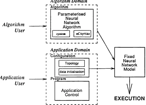
The Pygm alion's machine-independent neural network specification language, called /iC, is discussed in Chapter 4. The chapter commences with a general description of the nC programming features and then introduces the basic concepts that make nC a neural network dedicated language. It carries on with information on how to programme an algorithm and an application, the two basic elements to fully specify a neural network in nC. The chapter terminates with an examination o f the nC parser, designed to check if the user specification conforms with the language syntax.
neural network applications.
After the complete specification of the architectural framework, a mechanism to assess the suitability of the proposed model was necessary. So, chapter 6 examines the architectural simulations carried out in this research. Firstly it presents a short introduction to the simulator, describing the user interface provided and the data structure used. It then exhibits the simulation results based on the Back Propagation algorithm.
Chapter 7 investigates the implementation of the proposed architecture as VLSI chips. It firstly analyses the design approach taken and then provides a full description o f the cell library used in the project. The chapter then concludes discussing the results o f the Back Propagation layout design implemented using CMOS 2|im technology.
Chapter 8 is the assessment chapter. The four main elements o f the research - the nC
language, the generic neuron model and the corresponding VLSI architecture, the
simulator and the VLSI chip - are discussed, investigating their strengths and weaknesses.
Chapter 2
VLSI Architectures for Artificial Neural Networks
This chapter provides a review o f VLSI architectures fo r artificial neural networks. Neurocomputers are first classified into special-purpose and general-purpose. Then the chapter examines the fo u r architectures under analysis in the Esprit II Galatea project: the Siemens, Philips, INPG (In-stitut National Poly technique de Grenoble), and finally the UCL architec ture developed in this thesis.
2.1. Neurocom puters
As mentioned in Chapter 1, neural network models are evolving in such a way that con ventional computers will not be capable o f providing the necessary performance to exe cute more elaborate applications. Only highly parallel machines, with neural network
dedicated hardware, namely neurocomputers, will achieve the required performance to
execute applications such as speech recognition19,49,100. Therefore, many researchers are investigating different approaches for the development o f high performance neuro- computers.
A neurocomputer is essentially a parallel array o f interconnected processors that operate concurrently. Each processing element is primitive (that is, it can be an analogue neuron or a simple reduced instruction set - RISC - microprocessor) and may contain some local memory.
tially high performance. Special-purpose neurocomputer designers have studied various different technologies, including electronic (digital and analogue), optical and electro- optical47,49. General-purpose neurocomputers, on the other hand, are generalised, pro grammable neural computers for emulating a range o f neural network models. Conse quently, they tend to be slower than the special-purpose machines, but allow efficient ex perimentation with different network models. This approach is generally implemented using digital technology.
A review of current implementations in both special-purpose and general-purpose neuro- computers is presented in the next sections.
2.1.1. S p ecial-P u rp ose N eurocom p uters
The approach for special-purpose neurocomputer architectures is to directly implement a specific neural network model in hardware. Any neural network model could theoretical ly be chosen, although Kohonen64 and Hopfield5-* associative memory models are typi cally favoured, because of their simplicity in terms o f regular connectivity and processor’s functionality.
Designers have successfully built several examples of very high performance, special- purpose neurocomputers. This review will concentrate exclusively into the existent analogue and digital implementations. Information on current designs employing other technologies, like optical and even electrochemical, can be found in Hecht-Nielsen’s book49.
A n a lo g u e D e sig n s
Analogue electronic implementations o f neural networks typically employ physical struc tures that resemble the simplified mathematical model of the neuron’s state calculation:
N
sj^i ZSiXWij -Q).
i= l
low accuracy19. Nevertheless, analogue designs usually produce smaller circuits allow ing therefore more processors per chip, which is an important issue in the development of neurocomputers.
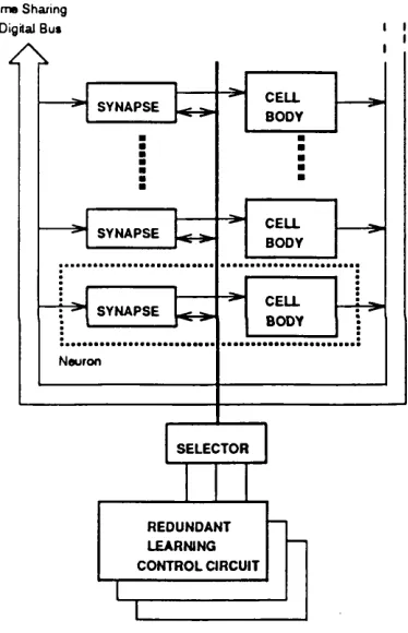
The circuit of Figure 2.1a illustrates the simpliest structure used in analogue implementa tions. It is a straightforward electronic implementation o f the simplified electrical model o f the biological neuron. Wires replace the input (dendrites) and output (axon) struc tures. Resistors model the synaptic connections between neurons, and the amplifier models the cell body by executing the threshold function. Inputs appear as current on the summing wire. Using these electronic neurons, a neural network can be implemented as a crossbar representation (Figure 2.1b). Outputs (vertical lines) A1-A4 are connected through resistors to the horizontal summing wires, which contain the weighted sum o f the output signals of other processing elements (PEs). Inverted input lines are also provided to be used when both positive and negative values are required.
output lines
Input (dendrites)
Resistors (synapses)
Amplifier (cell body)
Output (axon)
A1 A2 A3 A4
1
n
e
s
A2 A3 A4
A1
(a) Electronic Neuron (b) Interconnected Processing Elements
Figure 2.1: General View of a Special-Purpose Neurocomputer.
Many groups are working on analogue implementations of neural networks. Graf, Jackel and their colleagues at AT&T Bell Labs39-41’54' 56,69 have designed a number o f neural network chips. Their first implementation consisted of an analogue chip with a 22x22 matrix of fixed, microfabricated resistive synapses and off-chip amplifiers. The resistor matrix was fabricated on oxidised silicon substrates-54' 56, occupying an area of 88x88p/?z2. Another early design39 consisted of a fully interconnected array o f 256 on- chip amplifiers. The connections between amplifiers were made through fixed resistors, using the same microfabrication process utilised in the previous chip. The chip was designed in 2.5 fim CMOS technology occupying an area of 5.1x5.7mm . More recent designs that provide a certain degree o f programmability for the weight values include69:
• a hybrid analogue/digital chip, comprising 54 neurons fully interconnected through a programmable resistor matrix. The synaptic circuit is programmed by the contents of two RAM cells, providing excitatory, inhibitory and disabled connec tions40,41,56. Although this approach supports adjustable weight values, the use of RAM cells increases substantially the synaptic circuit size, losing, therefore, the main advantage of analogue designs. The chip was fabricated in 2.5 |im CMOS technology resulting in an area o f 6.1x6.1mm .
• a fully analogue design of an adjustable connection matrix composed of 1104 con nections. The matrix is arranged in an array of 46 inputs and 24 outputs. The chip, which does not include the amplifiers, was designed in 1.25 }im CMOS41. The synaptic circuit is based on dynamic weight storage, where the analogue weight value is stored as a charge on a capacitor. Dynamic weight storage grants much smaller synaptic circuits but, owing to the intrinsic dynamic characteristic, problems like charge leaks and data corruption are likely to occur if long hold times are re quired83.
Verleysen and his group at University Catholique de Louvain, B elgium 127' 129, are also developing analogue, special-purpose neurocomputers. Their synaptic circuit design fol lows a similar approach to the programmable, analogue/digital circuit developed by Graf. They also utilise RAM cells to programme the synaptic value but the circuit was im proved to overcome the problem of not attaining equal values for the excitatory and inhi bitory currents. The problem is avoided by using the same type o f transistor to sink and source current on the input line of the neural processor. This has been achieved by using two distinct lines to sum the currents: one for excitatory currents and another for inhibito ry currents129. The design of the neural processor had also to be modified in order to be adapted to two input current lines. To test the performance o f this new scheme, they have designed a small chip containing 14 neurons and 196 synapses.
A different approach, that uses pulse-stream arithmetic, is used by Murray and his group at University of Edinburgh82' 85. The architectural structure is also based on a fully inter connected network arranged in a 2-dimensional array of synapses, but signals flowing
through the network are actually a stream of pulses. Their main motivation for using pulse-stream form was its analogous relationship with biological neurons84. In the pulse-stream design, the neuron behaves as a switched oscillator, where the oscillator’s firing rate is controlled by the level of accumulated neural activity. Therefore, the neuron’s output state is represented by the output pulse frequency and each synapse determines the proportion of the input stream that will pass to the neuron input. Their first implementation consisted of a 3 |im CMOS chip, comprising a 10x10 synaptic ma trix, and 10 off-chip neurons. The synaptic circuit was based on a RAM, to store the synaptic weight, and on chopping clocks to form the pulse-stream input to the neuron. The basic component of the neuron was a voltage-controller oscillator (VCO) which is controlled by the charge on a capacitor. Due to the low level o f integration caused by the digital weight memory, a new design for the synapse circuit is being implemented, deriv ing from the dynamic weight storage technology82,84.
An Intel research group5 2 is working with floating gate, non-volatile, memory technolo
stored weight and generates a differential current proportional to the product. The dif ferential currents are then summed, transferred through a sigmoid function and finally ap pear at the neuron output as an analogue voltage. To adjust the weight value, an external intelligent controller must calculate the voltage to be applied to each synapse in order to attain the required weight value. The weights are addressed and modified one at a time. This technique affords electronic programmability at the expense o f demanding non standard fabrication process83. The Intel group produced a chip with 64 neurons and
10240 floating gate synapses, where 2048 are used for setting bias for each neuron, 4096 used to fully interconnect the neurons and the remaining 4096 to connect the 64 neurons to 64 independent inputs.
Finally, some other groups working with analogue implementations include: Agranat, developing circuits using charge coupled devices (CCD)7; Rossetto and his group at In- stitut National Polytechnique de G renoble106; and Goser and his team at University of D ortmund38.
The above examples demonstrate that analogue circuits are suitable for implementing small-scale, specialised neural network applications that can be integrated into one single chip86,135. This comes as an immediate consequence o f the fully connectivity approach used in all analogue systems. The data communication is perform ed with no multiplexing of signals, using dedicated wires for each necessary value that m ust be transmitted from one neuron to another. This scheme results in faster circuits but also makes the cascading of various chips very complex. Additionally, due to the native analogue characteristics, it is very difficult to produce two integrated circuits with the same features. On the other hand, analogue technology can grant smaller circuits, although in order to achieve small and programmable synaptic circuits, non standard processes are being used, such as the MNOS (metal nitride oxide silicon) technique for EEPRO M -based circuits. Then, to overcome some o f these intrinsic problems found with the analogue technology, many groups are inclined to follow the digital approach.
D ig ita l D e sig n s
development of high performance, digital special-purpose neurocomputers.
One o f the most well-known digital implementation is the W ISARD machine, developed by Aleksander and his group^'11. The WISARD architecture (W ilkie, Stoneham, Alek- sander Recognition Device) is an adaptive pattern recognition system designed specifically for image processing. The system employs statistical pattern-classification techniques to achieve impressive recognition and judgement capabilities. The design of the WISARD system centres on arrays o f RAM cells that operate as image discrimina tors. Each discriminator consists of K RAMs of N bits followed by a summation operator that counts the number of RAMs with output l 83. Therefore, the input pattern represents the N x K input image and the discriminator output indicates the similarity o f an input pattern with each of the previously training set. So, when submitted to input images, the system produces a response that expresses a "measure of confidence". The system digi tises the input image and stores it as a binary pattern in an image memory in which a sin gle bit represents each pixel. Recognition occurs when discriminators are trained with ex amples of objects (frames captured by a camera) that associate with specific classes (ac cording to the views of the object). The WISARD system has innumerable applications involving classification, such as: inspection and quality assurance, robot vision, identification and sorting.
Personnaz and Weinfeld *00,133 have also designed a digital VLSI architecture, in this case specialised in the fully connected Hopfield neural m odel53. The architecture was devised to maximally reduce the necessary silicon area per processor, sacrificing, to a certain extent, the communication speed. The network contains N identical neural pro cessors, each one with full arithmetic capability for learning and updating, and for storing the N relevant synaptic values. Because the architecture implements the Hopfield algo rithm, the state values are coded in one bit, considerably simplifying the communication and arithmetic calculations. The transmission of states among the processor is performed by a circular N x 1 bit shift register, as shown in Figure 2.2. Every neuron executes, simul
PE1 SR
PE2 SR
PE6SR W
-SRPE3
- SR -E---- SR - E
PE5 PE4
Figure 2.2: Pcrsonnaz & Wcinfeld’s interconnection strategy.
Another interesting architecture, which also relies on circular shift-registers for the inter communication structure, has been developed at Fujitsu Laboratories61. The architec ture, which executes the Back Propagation algorithm58*107’ 130, consists o f multiple pro cessing units (PU s)t, and trays to implement the cyclic shift register. Each tray is con nected to its two neighbours and functions as a container and a router for the data being transmitted. The basic structure of the architecture is depicted in Figure 2.3.
input hidden output i aYeI J^y^r _ layer_
Tray
Tray
Tray Tray
PU PU
PU
Artificial Neural Network
Architectural Im plem entation
Figure 2.3: The Fujitsu Basic Architecture.
The example in Figure 2.3 depicts a neural network composed o f four neurons in the in put layer, three in the hidden layer, and two in the output layer. The architectural imple mentation has four trays, three PUs, and no physical layer structure. Neurons at the same row (belonging to different layers) are mapped to the same tray and simulated succes sively by the associated PU. Therefore, each processing unit actually emulates more than one neuron. Each PU has a floating point multiplier, an adder and some local memory for programme and weight values. A prototype, called Sandy/8, has been developed using a
floating point digital signal processor as PU. The prototype consists o f 256 PUs, each with 2K words internal RAM and an external RAM o f 64K words. The tray circuit was implemented using gate-arrays. The prototype is connected to a host machine (Sun-3) and the estimated performance is o f 135 million connection updates per second. Since the system uses a (programmable) digital signal processor, other algorithms besides Back Propagation can also be programmed. Therefore, the architecture might also be con sidered o f general purpose.
A different architecture that is also dedicated to the Back Propagation neural model has been developed by a group at University o f Ancona, Italy101. The proposed architecture is composed o f a set o f elementary processing elements connected in a linear sequence, where every PE communicates only with its two nearest neighbours. The processing ele m ent is formed by three basic units: I/O, execution and control units. The I/O unit, that deals with the communication, contains 3 input and 3 output data busses, o f which two are used in the forward mode (left to right direction in the array) and one is used in the backward mode (right to left direction). The execution unit comprises the RAM memory for weights and inputs, an ALU able to perform add and multiply operations, a look-up table for the threshold function, and some registers to configure the network. Finally, the control unit controls the whole execution inside the neural processor. This "snake" archi tecture, as it is called, is a SIMD (Single-Instruction-stream, M ultiple-Data-stream) machine since every processor performs the same operations on different data. The sys tem can be configured in terms of number and width o f layers, and can be expanded to as many processors as necessary. A more recent work has been carried out by the same group where they have studied the feasibility o f restricting the weight values to power- of-two or sums o f powers-of-two, in order to reduce silicon area and multiplication time. They have performed some tests on a simple pattern recognition problem and have shown the feasibility o f the approach71.
tor5^. The architecture is dedicated to the implementation o f the recall phase, executing in hardware only the state calculation. Hence, all weight values have to be evaluated by simulation and then loaded into the system. The architecture, however, is very flexible, being able to realise any arbitrary network topology. The architectural structure is based on the assumption that the states are represented by firing frequencies and the weight is a stochastic pulse train which modifies the state frequency. With this approach, the multi plication computation can be implemented by AND gates, significantly reducing the sili con area. Two chips were designed to test the architectural approach. One chip contains the synaptic values, composed of a 32x32 matrix, and a stochastic pulse generator. The second chip implements 32 neurons, each comprising an integrator and a stochastic pulse generator.
As can be seen from the above examples, many research groups are developing special ised digital hardware for high performance execution of artificial neural models. Dif ferent approaches, to match the desired neural application, are being used for the topo logical distribution and for the processor’s configuration. Despite these dissimilarities, there is a common tendency among all the proposed architectural systems regarding the communication strategy. All of them use a localised communication plan in contrast to the fully connectivity found in analogue designs. Additionally, the processor’s structure is limited to one arithmetic unit, instead o f providing hardware circuitry to execute the neural algorithm with full parallelism, which is one o f the recognised powerful features attained by analogue circuits. The decision to apparently sacrifice the system’s perfor mance is due to the necessity to save silicon area and to produce expandable systems, as it is impossible, with current technology, to integrate large networks in one chip. Although this approach causes a moderate reduction in the efficiency o f the system, the loss is compensated by the simplicity of the processing element. As the processor’s hardware is developed to execute a specific algorithm, and as very high performance cells can be obtained with state-of-the-art technology, the final performance is generally very good.
2.1.2. G en eral-P urp ose N eurocom p uters
Artificial neural networks are still under great evolution, with many different algorithms being frequently developed. Yet, no neural model is applicable to all possible neural net work applications. Consequently, a flexible architecture, with the ability to implement a wide range of neural models and still afford higher performance than simulations on con ventional machines, is required. These architectures are called general-purpose neuro computers.
General-purpose neurocomputers are programmable machines that can support a wide spectrum of neural network models, thus providing a framework analogous to traditional computers.
General-purpose neurocomputers can be subdivided into commercial coprocessors
boards, and parallel processor arrays120. Commercial coprocessors usually consist of a
single floating-point or signal processing accelerator board, generally based on a power ful processor supplied with a large memory. These boards plug into the backplane of an IBM PC or interface to a SUN Workstation or a DEC VAX. Parallel processor arrays, on the other hand, are cellular arrays1 1 1 composed o f a large number o f primitive processing
units connected in a regular, and usually restricted, topology.
Accelerator boards, such as the HNC (Hecht-Nielsen Corporation) ANZA48, and the SAIC (Scientific Applications International) SIGMA-14, implement large networks of virtual neurons by means of an industry-standard signal processing chip or microproces sor (such as the MC68020 in the ANZA system), interconnected through a standard parallel broadcast bus such as the VMEbus. The physical processor is multiplexed across a large number o f virtual processing elements and virtual interconnections, demanding large memories to represent them. Performance comparisons between these products in volve capacity (the maximum size o f neural network) and speed (the time to process a neural network). For instance, the ANZA Plus4 8 supports 1M virtual processing ele
ments, with 1M interconnections. It can perform 1.500 connection updates per second during learning and 6 . 0 0 0 updates during recall.
by distributing the network through a larger number of processors, increasing therefore the final performance. Many different approaches are being followed, spanning from re plication of the single processor accelerator board, through transputer-based networks, to the more recent systems based on custom-designed neuro-processors.
The earliest commercially available neurocomputer, the TRW Mark III, and its improved version Mark IV49, were based on replicative accelerator boards. Mark III is composed o f a maximum of 15 boards, using a similar approach to the 68020-based ANZA board as the essential replicative unit. Another example o f this approach is the Computation Net work Environment (CONE) 2 4 , 4 5 developed at IBM ’s Scientific Center in Palo Alto.
CONE is based on the Network Emulation Processor (NEP), a cascadable board that acts as a coprocessor for a PC host. The NEP board is based on the 5 MIPS (million instruc tions per second) TMS320 fixed-point digital signal processor and up to 256 boards can be connected to the interprocessor communication bus (NEPBUS). The complete system is able to simulate 1M nodes with up to 4M connections and perform 30 to 50 network updates per second.
Other research institutions are applying arrays o f transputers to execute neural network applications. One of the first systems based on transputers was developed at the US Na tional Aeronautics and Space Administration’s Johnson Space Center in Huston, Texas. The system is called Neural Network Environment Transputer System (NNETS) 1 ®9 and
comprises forty 32-bit transputers interconnected via four full-duplex serial links. Other examples o f transputer networks for simulating neural network applications include: at the University o f Palermo, Italy, where a double linked ring topology has been chosen to interconnect 4, 8, 12, or 16 transputers77; at the University o f Marburgh, Germany,
where the ANNE (Another Neural Network Emulator) system has been developed78, which allows an arbitrary size for the transputer net without having to recompile existing programmes; at the University of Zurich, Switzerland, which uses a board (Levco Translink II card) of 4 transputers connected to a Macintosh computer to simulate neural nets29; and finally at Clarkson University, USA, where a board containing four tran sputers (called Quadputer and implemented by MicroWay) is used to execute Back Pro
pagation networks of various sizes, for image processing applications8. These
transputer-based systems are usually integrated to a programming environment tool, with a high level network specification language and graphical facilities. These programming tools help to overcome the common difficulties found in programming transputer sys
tems7 8 and provide a good environment for the simulation analysis.
Replicative boards and array of transputers have considerably increased the processing power for executing neural networks. However, the degree o f parallelism is still limited as many virtual neurons are mapped into a restricted number o f physical processors (pro cessing units). For real-time and more complex applications, a larger number o f process ing units is required in order to attain a higher degree of parallelism and much more dense systems. Hence, many research groups are developing their own custom designed neural chips, achieving more compact designs with a substantial number o f physical pro cessors.
These custom-designed chips follow two distinct approaches that can be classified as weight-based architectures, which are based on systolic array techniques, and neuron-based architectures, where the physical processors are based on the neuron’s functionali ty*
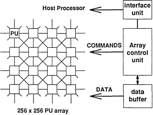
broadcasts commands to all processors; a data buffer memory; and an interface unit to communicate with the host computer. Each processing unit is essentially composed o f two versatile data transfer units, a one-bit ALU, and 8K bits o f local memory. In addi
tion, to increase the communicauon efficiency, the architecture provides three different mechanisms to perform data transfer between processors: connections to the nearest neighbour; connection through a programmed data transfer path; and communication via message passing. The AAP-2 architecture is able, through a folding mechanism, to simu late a network with up to 2 million connections.
H ost P r o c e sso r
COMMANDS
DATA PU
interface
unit
d a ta
buffer
Array
control
unit
256 x 256 PU array
Figure 2.4: System configuration for the NTT AAP-2 architecture.
Two additional examples of weight-based architectures are presented in more details in
section 2.2, namely the Siem ens1^4, ^ the Philips architectures27,21*.
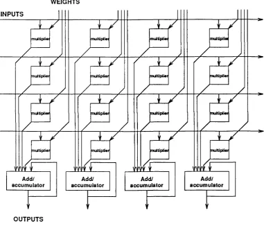
These systolic array architectures offer very fast computation of basic neural functions, like the vector-matrix multiplication required for the evaluation o f the weighted sum of input values. This is due to the fact that these systems focus on the synapse functionality. Consequently, the hardware is basically formed by a 2-dimensional array of multipliers,
used for processing the weighted values. As a direct effect from this hardware configuration, these architectures are not only limited to neural network implementations, being able to execute other signal processing applications, as in the case o f the Warp and its improved version, the iWarp machine2-*.
However, some drawbacks arise from using the matrix configuration. These systems are more suited to fully connected neural networks, achieving with these regular configurations their best performance. When non-regular network topologies are used, like sparsely connected networks, the resultant system efficiency decreases1-*2. The use o f high speed memories is also an important issue in these architectures, in order to af ford high rates of data transfer between the processor array and the memory bank. More over, due to the two-dimensional topology, these architectures are non-scalable, con straining the network size to the medium scale range. Indeed, the non-scalable nature of this topology prevents the construction o f a cost-effective network with a very large number of weight-based processors. Additionally, it binds the total number o f processors that can be integrated into one chip to the maximum number o f pads available in the fa brication technology. 1 0 5
Due to these intrinsic limitations of the weight-based architectures, a different approach
is being followed by many research groups, which are developing neuron-based architec
tures. Instead of focusing on the synapse functionality, these systems centre their atten tion into the neuron’s operations.
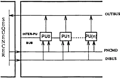
Another neuron-based general-purpose neurocomputer, named CNAPS - Connected Net work of Adaptive Processors, has been developed by Adaptive Solution Inc^*44. The CNAPS system consists of a number of simple, digital processing units, operating in a SIMD configuration. Communication is executed through broadcast busses that provide high-performance intercommunication. Each processor is actually connected to three glo bal busses (see Figure 2.5): an input, an output and a command bus (INBUS, OUTBUS and PNCMD respectively). There is also an inter-processor bus between adjacent processing units used to effect the arbitration algorithm for the output bus and to allow inter- processor data transfer.
PUO
T J
PU1 T~J
OUTBUS
. 3U(n T J
Figure 2.5: Adaptive Solution processor array system architecture.
Each processing unit is composed o f a simple arithmetic processor with an internal memory. Arithmetic operations are executed using fixed-point representation and internal busses are coded in 16 bits. The neural processor is optimised for traditional neural net work applications, but is general enough to implement classical digital signal processing and rule based processing44. The network o f processors is supervised by an external sequencer controller chip that specifies, via the command bus, the instruction that must be executed by all processors. Adaptive Solutions claims that for 1-bit weights, the max imum performance reaches 1 2 . 8 billion connections per second, without learning.