arXiv:0807.0310v1 [cond-mat.mes-hall] 2 Jul 2008
Influence of a single defect on the conductance of a tunnel point
contact between a normal metal and a superconductor
Ye.S. Avotina,1, 2 Yu.A. Kolesnichenko,1, 2 and J.M. van Ruitenbeek2
1
B.I. Verkin Institute for Low Temperature Physics and Engineering, National Academy of Sciences of Ukraine,
47, Lenin Ave., 61103, Kharkov,Ukraine.
2
Kamerlingh Onnes Laboratorium, Universiteit Leiden, Postbus 9504, 2300 Leiden, The Netherlands.
Abstract
We have investigated theoretically the conductance of a Normal-Superconductor point-contact in the tunnel limit and analyzed the quantum interference effects originating from the scattering of quasiparticles by point-like defects. Analytical expressions for the oscillatory dependence of the conductance on the position of the defect are obtained for the defect situated either in the normal metal, or in the superconductor. It is found that the amplitude of oscillations significantly increases when the applied bias approaches the gap energy of the superconductor. The spatial distribution of the order parameter near the surface in the presence of a defect is also obtained.
I. INTRODUCTION
Electron scattering by single surface [1] and subsurface [2] defects results in an oscillatory dependence of the Scanning Tunnelling Microscope (STM) conductance G on the distance,
r0, between the contact and the defect. These oscillations originate from the interference of
electron waves, which are scattered by the defect and reflected back by the contact. They have the same period (G ∼ sin (2kFr0 +δ), kF is the Fermi wave vector) as the Friedel oscillations [3] of the local electron density of states in the vicinity of a scatterer. For subsurface point-like defects the oscillatory dependence of the conductance in a STM-like geometry has been investigated theoretically in Refs. [4, 5, 6, 7, 8].
Although defects below a metal surface can be ’visible’ in STM data for up to ten in-teratomic distances [9, 10], the amplitude of the quantum oscillations in the conductance become very small with increasing defect depth. An effective way to enhance the STM sensitivity to such oscillation effects is to use a superconducting tip [11]. In Ref. [12] using a low-temperature STM with normal metal tungsten tips and superconducting niobium tips, the formation of electron standing waves near surface defects and step edges on a Au (111) surface have been observed. It was demonstrated that the amplitude of conductance oscil-lations is significantly enhanced when a superconducting tip is used, and when the applied bias |eV| is close to the gap energy ∆0 of the superconductor.
The investigation of various defects in superconductors with STM is of interest by it-self. For example, in Ref. [13] a bound state near a magnetic Mn adatom on the surface of superconducting Nb was observed by STM. The effect of single Zn defects on the supercon-ductivity in high-Tc superconductors was investigated in Ref. [14], and the manifestation
of d-wave symmetry of the order parameter was observed in the quasibound state near the defect.
The listed reasons define the interest of theoretical investigations on the conductance of normal metal - superconductor (NS) tunnel contacts of small lateral size, in the vicinity of which a single defect is placed. The authors of Ref. [15] considered the conductance of a NS contact of finite size at low temperatures and for voltages |eV| < ∆0 using the
tunnelling Hamiltonian approximation. They found that, when the radius a of the contact is smaller then the Fermi wave length λF, the conductance of a NS point-contact becomes
Gns = (h/2e2)G2nn ∼ a8, where Gnn is the conductance of the contact in the normal state [15]. This dependence is fundamentally different from the result of a quasiclassical theory [16], valid for a ≫λF.
The conductivity of large (a ≫ λF) ballistic NS contacts in the presence of a ‘planar defect’ was investigated theoretically in several papers [21, 22, 23, 24]. In these papers a planar NS structure and aδ-functional potential barrier, playing the role of the defect, have been considered, from which ‘geometrical’ resonances resulted due to combined Andreev and normal reflections.
In order to describe the effect of isolated point-like defects in a superconductor on the STM conductance usually calculations of the local density of statesn(r) are used (for a review, see [25]), where it is assumed that the conductance of the small tunnel contact is proportional to the local density of electron states. While for subsurface defects this assumption remains qualitatively valid, it does not permit a correct description of the details of the conductance oscillations because the bulk electron density of states around the defect is modified by reflection from the interface, r∈Σ, and in the limit of zero tunnelling probability we have
tunnel junction in the presence of the defect should be considered.
In this paper we present the results of a theoretical investigation of the conductance of a NS point contact (with a ≪ λF ) in the tunnelling limit and we analyze the quantum interference effects originating from the scattering of quasiparticles by a point-like defect. Analytical expressions are obtained for the dependence of the conductance on the position of the defect and on the applied voltage, for the defect situated in the normal metal or in the superconductor.
II. MODEL AND BASIC EQUATIONS
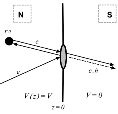
Our model is presented in the Fig.1. The normal and superconducting half-spaces are separated by an infinitely thin dielectric interface, which has an orifice of radius a. The potential barrier in the plane of interface z = 0 is taken to be a δ−function, U(r) =
U0f(ρ)δ(z), where ρ is the value of the radius vector ρ in the plane z = 0. The function
f(ρ)→ ∞ in all points of the plane except in the contact (ρ < a) , where f(ρ) = 1. In the point r0 a nonmagnetic defect described by a spherically symmetric potential D(|r−r0|)
is placed. A voltage V is applied between the two sides of the contact. We assume that the transmission probability |t| of electrons through the barrier in the orifice is small (|t| ≈
~2kF/m∗
U0 ≪ 1, m∗ is effective electron mass). In that case the applied voltage drops
entirely over the barrier and the electric potential can be described by a step function,
V (z) = V Θ (−z) with V a constant. Based on the same reasoning we use a step function for the superconducting order parameter ∆ (r) = ∆ (r) Θ (z). We consider the case of low temperatures and in the calculations takeT = 0.At zero temperature a tunnel current flows through the contact for |eV|>∆ . The applied bias is assumed to be small on the scale of the Debye frequency ωD and the Fermi energy εF, |eV| ≪~ωD ≪εF.
For definiteness we consider electron tunnelling from the normal half-space (z <0) to the superconducting half-space (z >0), i.e. eV > 0. In order to evaluate the total current through the contact,I(V), and the differential conductance, G(V) =dI(V)/dV, we should find the current density jk(r) of quasiparticles with momentum k at z > 0, formed by electrons transmitted through the contact. The current density jk(r) can be expressed in terms of the coefficients uk(r) andvk(r) of the canonical Bogoliubov transformation [17, 18]
jk(r) =
e~
m∗ Im [uk(r)∇u ∗
k(r)fF(Ek)−vk(r)∇v
∗
k(r)fF(−Ek)], (1)
wherefF(E) is the Fermi function, which atT = 0 is simply the unit step-function,fF(E) =
Θ (E).The functionsuk(r) andvk(r) satisfy to the Bogoliubov-de Gennes (BdG) equations [19]
− ~ 2
2m∗∇
2
−εF +D(|r−r0|)
uk(r) + ∆ (r)vk(r) = Ekuk(r), (2)
−
− ~ 2
2m∗∇
2
−εF +D(|r−r0|)
vk(r) + ∆
∗
(r)uk(r) = Ekvk(r).
Eqs. (2) may be interpreted as wave equations for a two-component ‘wave function’,
b ψk=
uk
vk
FIG. 1: Model of the contact. The point-like defect is situated in the normal half-space. The elec-tron trajectories in the normal metal and the trajectories of ‘elecelec-tron-like’ and ‘hole-like’ excitations in the superconductor are shown schematically.
of quasiparticles with energyEk.The conditions, which connect the vectorψbk in the normal metal (ψbnk) and in the superconductor (ψbsk) at the interface z = 0 are
b
ψnk(ρ,0) =ψbsk(ρ,0) =ψbk(ρ,0) (4)
∂
∂zψbsk(ρ,0)− ∂
∂zψbnk(ρ,0) =
2m∗
~2 U0f(ρ)ψbk(ρ,0) (5) The order parameter in the superconductor should be determined from the self-consistently condition
∆ (r) = γ X
k,Ek<~ωD
uk(r)v
∗
k(r) [1−2fF(Ek)], (6)
∆ (z →+∞)→∆0, (7)
where the constant ∆0 can be chosen real; γ is the pair potential constant. It can be easily
shown [17] that Eq. (1) combined with the self-consistently condition (6) automatically satisfies to the continuity equation
divX k
jk(r) = 0. (8)
superconducting half-space. For this surface we choose a half-sphere of large radiusr≫r0, ξ0
(ξ0 is the coherence length of the superconductor) centered at the contact r = 0. On this half-sphere we assume ∆ (r) = ∆0 and hence Ek =
p
ξ2k+ ∆20, where ξk =~2k2/2m
∗
−εF is the kinetic energy measured from the Fermi level. The conductance G(V) of the contact (at T = 0) is given by
G(V) = 4πr e2N(0)
Z dΩ
4πΘ (z)
∞
Z
−∞
dξk
Z dΩ
k
4π Θ (kz) (rjk(r))δ(Ek−eV). (9)
wheredΩ anddΩkare elements of solid angle in the real and momentum spaces, respectively,
N(0) is the density of states for one direction of spin.
III. SOLUTION OF THE BOGOLIUBOV - DE GENNES EQUATION
Generally, a self-consistent solution of Eqs. (2) can be found only numerically. Such solution must fulfil the condition of conservation of the total current I through any surface overlapping the contact, in spite of the spatial dependence of the order parameter. In order to simplify the task we will exploit the condition of a small barrier transparency and find an analytical solution of Eqs. (2) using the approximation of a constant order parameter ∆ (r) = ∆0Θ (z).By means of this solution the coordinate dependence of ∆ (r) can be found
(see Appendix).
In this section we generalize the method developed in the papers [4, 20]. We search the solutions of Eqs. (2) as an expansion into a series over the small transmission probability
|t| ∼1/U0,
b
ψk(r) = ψbk0(r) +ψbk1(r) +. . . , (10) where ψbk0(r) satisfies the zero-boundary condition at z = 0, and ψbk1(r) ∼ 1/U0. For the calculation of the current in leading approximation in the transmission coefficient (I ∼1/U2
0)
it is enough to find the first correction ψbk1(r). Substituting the expansion (10) into the boundary conditions (4), (5) we find that the function ψbk1(r) satisfies the condition of continuity at z = 0, and its value at z= +0 (in the superconducting half-space) is given by the relations
usk1(ρ,0) =
~2
2m∗
U0f(ρ)
∂
∂zunk0(ρ,0) ; vsk1(ρ,0) = 0. (11)
The boundary condition does not contain Andreev reflections, which appear in the next approximation in 1/U0 [30]. Thus, we will not consider Andreev resonances, which were
analyzed in Refs. [21, 22, 23, 24] for a one-dimensional model.
The quasiparticle scattering by the defect will be taken into account by perturbation theory in the strength of the interaction with the defect. First, we find the solution of Eqs. (2) for the contact without defect.
Let us consider an electron with energy Ek > ∆0, which moves towards the interface from the normal metal. When D(r) = 0 (the defect is absent) and 1/U0 = 0 (the interface
is impenetrable for electrons), in the normal half-space we have
unk0(r) =ei
κρ
eikzz
−e−ikzz
where k= (κ,kz), kz =kcos(ϑ), ϑ is the angle between the vector k and thez axis, and κ is the component of the wave vector parallel to the interface.
Making use of the Fourier transform of the bψk(r) components over the coordinate ρ in the plane parallel to the interface,
b
ψk1(ρ, z) =
∞
Z
−∞
dκ′Ψbk1(κ
′
, z)eiκ′ρ
, (13)
and finding Ψbk1(κ
′
,0) from the simplified boundary condition (11), we find the solution of Eqs. (2) in the superconducting half-space
uk1(r) = t(kz) 1
u2 0−v02
h
u20ϕ(+)0 (r) +v02ϕ(0−)(r)i, (14)
vk1(r) =t(kz)
u0v0
u2 0−v02
h
ϕ0(+)(r) +ϕ0(−)(r)i, (15)
where
ϕ(0±)(r) = ± 1 (2π)2
∞
Z
−∞
dκ′eiκ′ρ
∞
Z
−∞
dρ′e
i(κ−κ′)ρ′
f(ρ) e
±ik(z±)z
, (16)
kz(±)=
√
2m∗
~
εF −
~2κ2
2m∗ ±
q E2
k−∆20
1/2
, (17)
u20= 1−v02 = 1 2
1 + ξk
Ek
(18)
t(kz) = ~2kz/im∗
U0 is the amplitude of electron wave after tunnelling through the
ho-mogeneous barrier with a large U0. The functions uk1(r) and vk1(r) contain the sum of two solutions ϕ(0±)(r) of Eqs. (2), which correspond to ‘electron-like’ (k(+)z > kzF =
1
~
p
2m∗
(εF −~2κ2/2m∗)) and ‘hole-like’ (k(
−)
z < kzF) quasiparticles having a positive z -component of the group velocity vg =dEk/~dk.
For a small radius of the contact (in the limita →0) the function (16) takes the form [8]
ϕ(0±)(r, k) = k
(±)
a2cosθ
2 h
(1) 1 (k(
±)
r), (19)
k±
(Ek) =
√
2m∗
~
εF ±
q E2
k−∆20
1/2
. (20)
Here, h(1)1 (x) is the spherical Hankel function of the first kind.
In the presence of the defect the functions uk1(r) and vk1(r) can be found in first ap-proximation in the potential D(|r−r0|) of electron-impurity interaction by means of the
Eqs. (2).
1) If the defect is situated in the normal half-space the functionsuk1(r) andvk1(r) in the superconductor have the same form as Eqs. (14), (15) in which the amplitude t(kz) must be replaced by the value
e
t(kz) =t(kz) + 4π
2m∗
k
~2 gt(k)unk0(r0)h (1)
where g is the constant of the electron interaction with the defect
g =
Z
drD(|r−r0|). (22)
In order to obtain Eq.(21) we assume that the characteristic radius of the scattering potential is much smaller than the Fermi wave lengthλF (point defect). This condition permits taking the functions unk0(r) and h
(1)
1 (kr) outside the integral at the pointr=r0. The variations in
the amplitudes of the ‘wave functions’ uk1(r) andvk1(r) result from the fact that the wave incident to the contact is a superposition of a plane wave and a spherical wave that comes from the scattering by the defect.
2) If the defect is situated inside the superconductor, the additions ∆uk1(r) and ∆vk1(r) to the functions (14), (15) due to the defect scattering take the form
∆uk1(r) =
2πm∗
g
~2
1
v2 0−u20
∞
Z
−∞
dκeiκ(ρ−ρ0)
1
k(+)z
u0sin kz(+)z
eik(+)z z
[u0uk1(r0)−v0vk1(r0)]
+ 1
kz(−)
v0sin k(
−)
z z
e−ik(z−)z
[u0vk1(r0)−v0uk1(r0)]
; (23)
∆vk1(r) =
2πm∗
g
~2
1
v2 0 −u20
∞
Z
−∞
dκeiκ(ρ−ρ0)
1
kz(+)
v0sin k(+)z z
eik(+)z z
[u0uk1(r0)−v0vk1(r0)]
− 1
kz(−)
u0sin k(
−)
z z
e−ikz(−)z
[u0vk1(r0)−v0uk1(r0)]
. (24)
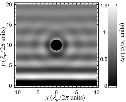
It is known that the order parameter ∆ (r) displays Friedel-like oscillations near a defect [26, 27] or a surface [28, 29]. The current through the tunnel contact I is defined by the average value of ∆ (r), which coincides with ∆0. In the Appendix we analyze the spatial
dependence of ∆ (r) near the surface of the superconductor, in the vicinity of which a non-magnetic defect is placed (at the distance less than the coherence length ξ0). Figure 2 illustrates the results of these calculations. An inhomogeneous spatial distribution of the order parameter is visible. We removed from the plot the region of radius λF (black circle) near the defect where Eq. (A9) is not valid.
IV. CONDUCTANCE OF THE CONTACT
By means of the solutions of the BdG equations, which have been obtained in previous section, we calculated the conductance Gof the NS tunnel point contact. In linear approxi-mation in the electron-defect interaction constantg the conductance G can be presented as the sum of two terms,
G(V, r0) =G0ns(V) + ∆Gosc(V, r0), eV >∆0. (25)
The first term, G0ns(V), in Eq. (25) is the conductance of the NS tunnel point contact in the absence of the defect
G0ns(V) =G0nn
eV q
(eV)2−∆2 0
; G0nn =
2e2a4m∗
ε3
F 9π~3U2
0
-10 -5 0 5 10
0 5 10 15 20
0 0.5 1. 1.5
(
F/2 units)
x
λ
π
(
/2
u
n
it
s)
F
y
λ
π
(
)
0
(
u
n
it
s)
∆
∆
∆
r
FIG. 2: Real space image of ∆ (r)/∆0 near the surface of the superconductor in the plane passing
through the defect which has been obtained by using Eq. (A9), and the parameters z0 = 10λF,
ξ0 = 104 λ
F,eg= 4π.
where G0nn is the conductance of a contact between normal metals, which is multiplied by the normalized density of states of the superconductor at E =eV in Eq. (26). The second term describes the oscillatory dependence of the conductance on the distance between the contact and the defect.
If the defect is situated in the normal metal half-space ∆Gosc(V, r0) is given by
∆Gosc(V, r0) =−G0ns(V) 12
πeg
λF
r0
2
(kFz0)2j1(kFr0)y1(kFr0), (27)
where
e
g = 2πm
∗
kF
~2 g (28)
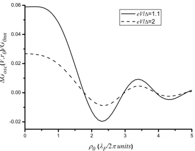
is the dimensionless electron-defect interaction constant, jl(x) and yl(x) are the spherical Bessel functions of the first and the second kind [31], and λF = ~/√2m∗εF . In Fig.3 dependencies of ∆Gosc(V, r0) on the distance ρ0 are shown for two values of the biaseV,one
of which is very close to the gap energy (eV /∆0 = 1.1),and the second one iseV = 2∆0.The
figure illustrates the increasing amplitude of the conductance oscillations near eV ≃∆0.
For the defect in the superconducting half-space the oscillatory part of the conductance consists of two terms
∆Gosc(V, r0) =−G0ns(V) 12
πeg
λ r0
2
(kFz0)2
X
α=±
ψα(eV)j1(kαr0)y1(kαr0), (29)
where
ψ±=
u0
v0 , k
±=
√
2m∗
~
εF ±
q
(eV)2−∆2 0
1/2
FIG. 3: Dependence of the normalized oscillatory part of the conductance ∆Gosc/G0ns, Eq. (27), on the distance ρ0 between the defect and the contact axis for two values of the applied voltage. The defect is situated in the normal metal at a depth z0 = 5λF. The dimensionless constant of interaction is taken aseg= 0.01.
In Eqs. (26)-(29) we neglected all small terms of the order of ∆0/εF andeV /εF . Nevertheless we kept the second term in square brackets in the formula fork± (see, Eq.(30)) because for
a relatively large r0, (
p
(eV)2−∆2
0/εF)(r0/λF)≃1, the phase shift of the oscillations may be important. In Fig. 4 we show the difference between the dependencies of the normalized oscillatory parts of the conductance ∆Gosc/G0ns on the distance ρ0 for a contact between
normal metals (∆0 = 0) and for a NS contact. An observable shift of the conductance
oscillations results from the voltage dependence of wave vectors k± (30).
V. CONCLUSION
Thus, we have analyzed the conductance G of a tunnel NS point contact with a radius
a smaller than the Fermi wave length λF, at low temperatures (T = 0) and for applied bias
eV larger than the gap energy of the superconductor ∆0.The effect of quantum interference
of quasiparticles scattered by a single defect situated in the vicinity of the contact has been taken into account. We have shown that in leading approximation in the parameters
eV /εF ≪ 1, ∆0/εF ≪ 1 the conductance of a small NS contact is G0ns = G0nnNs(eV), Eq. (26), i.e., the product of the conductance of the same contact between normal metals,
G0nn ∼ a4, and the normalized density of states of the superconductor Ns(eV), similar as for a planar tunnel contact. Although such result is not unexpected and has been confirmed by experiment [11], for a contact of radiusa < λF it was not obvious and it is first obtained in this paper.
If the defect is situated in the normal metal the conductance displays oscillations, the period of with is defined by the Fermi wave vector, ∆Gosc(V, r0) ∼ sin 2kFr0 at kFr0 ≫ 1
FIG. 4: The dependence of the oscillatory parts of the conductance ∆Gosc/G0 (29) on the distance
ρ0 between the defect and contact axis for the contact between normal metals (∆G(oscnn)/G0nn) and a NS contact (∆G(oscns)/G0ns). The defect is situated in the right metal (the superconductor) at a depth 10λF;eV /∆0= 5; eg= 0.01.
in oscillations of the transmission coefficient. The underlying principle here is similar to resonance transmission through a two-barrier system.
In the superconductor the electron wave incident on the contact from the normal metal is transformed into a superposition of ‘electron-like’ and ‘hole-like’ quasiparticles. In the case of location of the defect in the superconducting half-space quantum interference takes place between partial waves transmitted and those scattered by the defect, for both types of quasi-particles independently (Eq. (29)). Although the difference between wave vectors k(±)
(eV) of ‘electrons’ and ‘holes’ is small the shift k(+)−k(−)
r0between the two oscillations should
be observable (Fig. 4).
Appendix: Oscillations of the order parameter near the surface in the presence of a defect.
When calculating the conductance to first order in the transmission probability we should know the order parameter ∆ (r) in the limit of a nontransparent interface (surface),U0 → ∞.
According to Ref. [32],
∆∗(r) = γT
∞
X
n=−∞
Fω+(r,r) Θ (ωD −ω), (A1)
where ω = πT (2n+ 1) are the Matsubara frequencies. The Fourier components Gω(r,r′) and F+
defect potential have the form
iω−~
2∇2
2m∗ −εF
Gω(r,r
′
) + ∆ (r)Fω+(r,r′) = δ(r−r′) (A2)
iω+ ~
2∇2
2m∗ +εF
Fω+(r,r′) + ∆∗
(r)Gω(r,r
′
) = 0.
For a homogeneous superconductor ∆ (r) = ∆0 = const. and the solutions Gω(r,r
′
) =
G(0)ω (r−r′) and Fω+(r,r
′
) =Fω+(0)(r−r′) of Eqs.(31) can be found to be
G(0)ω (r−r′) = −πN(0)
kFr
"
coskFr+
iω p
∆2 0 +ω2
sinkFr
#
exp
−vr
F~
q
∆2 0+ω2
,(A3)
Fω+(0)(r−r′) = πN(0) ∆
∗
0
p
∆2 0+ω2
sinkFr
kFr exp
−vr
F~
q
∆2 0 +ω2
, (A4)
where r =|r−r′
|, vF is the Fermi velocity, ω ≪εF. For the semi-infinite superconducting half-space any component of the matrix Green function
b
G(ωs)(r,r′) = G
(s)
ω (r,r′) Fω(s)(r,r′)
Fω+(s)(r,r′) −G(−sω) (r ′
,r)
!
(A5)
can be written as
b
G(ωs)(r,r′) =Gb(0)ω (r−r′)−Gb(0)ω (r−er′), (A6) whereer′
= (x′
, y′
,−z′
).Equation (A6) is exact and it provides the zero value of ∆ (r) at the surface z = 0. The fact that the order parameter vanishes at the nontransparent interface can by seen from Eq.(6).
The Green’s function for the superconducting half-space in the presence of the point defect can be found from the Dyson equation
b Gω(r,r
′
) =Gb(s)
ω (r,r
′
) +
Z
dr′′Gb(s)
ω (r,r
′′
)D(|r′′−r0|)τ3Gbω(r
′′
,r′), (A7)
where τ3 is the Pauli matrix. Making use of the small radius of the defect potential in the
first order approximation in the interaction constant g (22) we obtain
Fω+(r,r) =Fω+(s)(r,r′) + (A8)
ghFω+(s)(r,r0)G(ωs)(r0,r
′
) +G(−sω) (r0,r)Fω+(s)(r0,r
′
)i.
As a first step for the self-consistent solution, the functions G(0)ω (r−r′) (31) and
Fω+(0)(r−r′) (31) may be used. At T → 0 the summation over Matsubara frequencies in Eq.(A1) can be replaced by an integration. Substituting the Eqs.(31), (31) into Eq. (A6) and using Eq.(A8) we find the space distribution of the order parameter (A1) in the next (after ∆ = ∆0 = const.) approximation.
∆ (r) = ∆0
1−sin 2kFz 2kFz
ln−1
2ωD ∆0
K
2πz ξ0 ;
ωD ∆0
+ (A9)
1 4πegln
−1
2ωD ∆0
sin 2kFs0
2 (kFs0)2 K
2πs0
ξ0 ; ωD ∆0
+sin 2kFse0 2 (kFes0)2
K
2πes0
ξ0 ; ωD ∆0
−sinkkF2(s0+es0)
Fs0se0
K
π(s0+es0)
ξ0 ; ωD ∆0
Here
K(a;b) =
arshZ b
0
dte−acht
, (A10)
s0 = |r−r0|; es0 = |r−er0|, and ξ0 = ~vF/π∆0 is the coherence length. At ab ≫ 1, K(a;b)≃K0(a), the modified Bessel function [31]. The Eq.(A9) is valid at distances from
the defect larger than the characteristic radius of the potential D(|r−r0|).The correction
to the constant value of the order parameter ∆0 decreases at small distancesr ≪ξ0 from the
surface or the defect according to a power law, and vanishes exponentially (∼ e−2πr/ξ0
) at larger distancesr≫ξ0.A grey-scale plot of ∆ (r) obtained by means of Eq.(A9) is presented in Fig. 2. In the plot we used an unrealistically large value of the constant eg in order to show the influence on the order parameter the defect and the surface in the same plot. For realistic valueseg ∼0.01 the spatial oscillations of ∆ (r) resulting from the scattering by the defect have a much smaller amplitude than the second term in the braces of Eq.(A9). The matching procedure can be continued when we put ∆ (r) of Eq.(A9) into Gor’kov’s equations (Eqs.(31)) or BdG equations (2). Unfortunately, starting with this step the solutions may be obtained only numerically.
Acknowledgments
One of us (Yu.K) would like to acknowledge useful discussions with A.N. Omelyanchouk, E.V. Bezuglyi, and S.V. Kuplevakhsky. This research was supported partly by the pro-gram ”Nanosystems nanomaterials, and nanotechnology” of National Academy of Sciences of Ukraine and Fundamental Research State Fund of Ukraine (project F 25.2/122).
[1] M. F. Crommie, C. P. Lutz, and D. M. Eigler, Science 262, 218 (1993).
[2] M. Schmid, W. Hebenstreit, P. Varga and S. Crampin, Phys. Rev. Lett., 76, 2298 (1996). [3] J. Friedel, Nuovo Cimento, 7, 287 (1958).
[4] Ye. S. Avotina, Yu. A. Kolesnichenko, A.N. Omelyanchouk, A.F. Otte, and J.M. Ruitenbeek, Phys. Rev. B 71, 115430 (2005).
[5] Ye. S. Avotina, Yu. A. Kolesnichenko, A.F. Otte, and J.M. Ruitenbeek, Phys. Rev. B, 74, 085411 (2006).
[6] Ye. S. Avotina, Yu. A. Kolesnichenko, S.B. Roobol and J.M. Ruitenbeek, Fiz. Nizk. Temp.,
34, 286 (2008).
[7] Ye. S. Avotina, Yu. A. Kolesnichenko, A.F. Otte, and J.M. Ruitenbeek, Phys. Rev. B 75, 125411 (2007).
[8] Ye. S. Avotina, Yu. A. Kolesnichenko, and J.M. Ruitenbeek, J. Phys.: Condens. Matter, 20,
115208 (2008).
[9] N. Quaas, M. Wenderoth, A. Weismann, R.G. Ulbrich and K. Sch¨onhammer, Phys. Rev. B
69, 201103(R) (2004).
[10] N. Quaas, PhD thesis, G¨ottingen University (2003).
[11] S. H. Pan, E. W. Hudson, and J. C. Davis, Appl. Phys. Lett.,73, 2992 (1998).
[13] Ali Yazdani, B. A. Jones, C. P. Lutz, M. F. Crommie, D. M. Eigler, Science,275, 1767 (1997) [14] S. H. Pan, E. W. Hudson, K. M. Lang, H. Eisaki, S. Uchida, and J. C. Davis, Nature, 403,
746 (1999).
[15] E. Prada, and F. Sols, Eur. Phys. J. B40, 379 (2004).
[16] A.V. Zaitsev, Zh. Eksp. Teor. Fiz., 86, 1742 (1984) [Sov. Phys. JETP59, 1015 (1984)]. [17] A. V. Svidzinskii, Spatially Inhomogeneous Problems in the Theory of Superconductivity (in
Russian), Nauka, Moscow (1982).
[18] M. Hard, S. Datta, and P.F. Bagwell, Phys. Rev. B, 54, 6557 (1996).
[19] P. G. de Gennes, Superconductivity of Metals and Alloys (W.A. Benjamin, Inc. New York, 1966).
[20] I. O. Kulik, Yu. N. Mitsai, and A. N. Omelyanchouk, Zh. Exp. Teor. Fiz., 63, 1051 (1974). [21] A. Hahn, Phys. Rev. B, 31, 2816 (1985).
[22] P. C. van Son, H. van Kempen, Phys. Rev. B, 37, 5015 (1988). [23] R. A. Riedel, P. F. Bagwell, Phys. Rev. B, 48, 15198 (1993). [24] S. Chaudhuri, P. F. Bagwell, Phys. Rev. B,51, 16936 (1995).
[25] A. V. Balatsky, I. Vekhter, and Jian-Xin Zhu, Rev. Mod. Phys. 78, 373 (2006). [26] A. L. Fetter, Phys. Rev.,140, A1921 (1965).
[27] M. E. Flatt´e, J. M. Bayers, Phys. Rev. B,56, 11213 (1997). [28] R. G. Boyd, Phys. Rev., 167, 407 (1968).
[29] K. Tanaka, F. Marsiglio, Physica C, 284, 356 (2003).
[30] G.E. Blonder, M. Tinkham, T.M. Klapwijk, Phys. Rev. B, 25, 4515 (1982).
[31] M. Abramowitz, and I.A. Stegun, ” Handbook of mathematical functions”, National Bureau of Standards (1964).