1.
General description
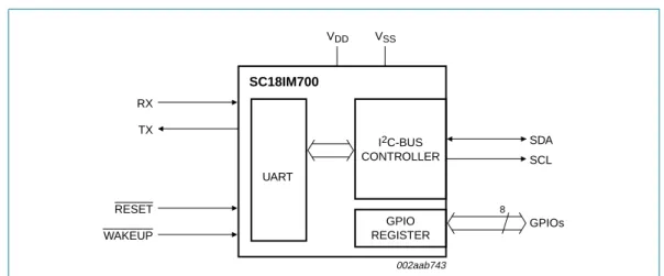
The SC18IM700 is designed to serve as an interface between the standard UART port of a microcontroller or microprocessor and the serial I2C-bus; this allows the microcontroller
or microprocessor to communicate directly with other I2C-bus devices. The SC18IM700
can operate as an I2C-bus master. The SC18IM700 controls all the I2C-bus specific
sequences, protocol, arbitration and timing. The host communicates with SC18IM700 with ASCII messages protocol; this makes the control sequences from the host to the
SC18IM700 become very simple.
2.
Features
n UART host interface n I2C-bus controller
n Eight programmable I/O pins
n High-speed UART: baud rate up to 460.8 kbit/s n High-speed I2C-bus: 400 kbit/s
n 16-byte TX FIFO n 16-byte RX FIFO
n Programmable baud rate generator n 2.3 V and 3.6 V operation
n Sleep mode (power-down)
n UART message format resembles I2C-bus transaction format
n I2C-bus master functions
n Multi-master capability
n 5 V tolerance on the input pins
n 8 N 1 UART format (8 data bits, no parity bit, 1 stop bit) n Available in very small TSSOP16 package
3.
Applications
n Enable I2C-bus master support in a system
n I2C-bus instrumentation and control
n Industrial control n Medical equipment n Cellular telephones n Handheld computers
SC18IM700
Master I
2C-bus controller with UART interface
4.
Ordering information
5.
Block diagram
Table 1. Ordering information
Type number Package
Name Description Version
SC18IM700IPW TSSOP16 plastic thin shrink small outline package; 16 leads; body width 4.4 mm
SOT403-1
Fig 1. Block diagram of SC18IM700
SC18IM700 I2C-BUS CONTROLLER 002aab743 VDD UART SCL SDA GPIO REGISTER GPIOs RX TX WAKEUP 8 RESET VSS
SC18IM700_2 © NXP B.V. 2007. All rights reserved.
Product data sheet Rev. 02 — 10 August 2007 3 of 22
NXP Semiconductors
SC18IM700
Master I2C-bus controller with UART interface
6.
Pinning information
6.1 Pinning
6.2 Pin description
Fig 2. Pin configuration for TSSOP16
SC18IM700IPW GPIO0 GPIO7 GPIO1 GPIO4 RESET GPIO5 VSS WAKEUP GPIO2 VDD GPIO3 GPIO6 SDA TX SCL RX 002aab798 1 2 3 4 5 6 7 8 10 9 12 11 14 13 16 15
Table 2. Pin description
Symbol Pin Type Description
GPIO0 1 I/O programmable I/O pin GPIO1 2 I/O programmable I/O pin RESET 3 I hardware reset input
VSS 4 - ground
GPIO2 5 I/O programmable I/O pin GPIO3 6 I/O programmable I/O pin SDA 7 I/O I2C-bus data pin SCL 8 O I2C-bus clock output
RX 9 I RS-232 receive input
TX 10 O RS-232 transmit input
GPIO6 11 I/O programmable I/O pin
VDD 12 - power supply
WAKEUP 13 I Wake up SC18IM700 from Power-down mode. Pulling LOW by the host to wake up the device. A 1 kΩ resistor must be connected between VDD and this pin.
GPIO5 14 I/O programmable I/O pin GPIO4 15 O programmable I/O pin GPIO7 16 O programmable I/O pin
7.
Functional description
The SC18IM700 is a bridge between a UART port and I2C-bus. The UART interface
consists of a full-functional advanced UART. The UART communicates with the host through the TX and RX pins. The serial data format is fixed: one start bit, 8 data bits, and one stop bit. After reset the baud rate defaults to 9600 bit/s, and can be changed through the Baud Rate Generator (BRG) registers.
After a power-up sequence or a hardware reset, the SC18IM700 will send two continuous bytes to the host to indicate a start-up condition. These two bytes are 0x4F and 0x4B; ‘OK’ in ASCII.
7.1 UART message format
The host initiates an I2C-bus data transfer, reads from and writes to SC18IM700 internal
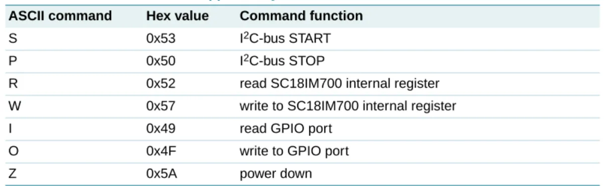
registers through a series of ASCII commands.Table 3 lists the ASCII commands supported by SC18IM700, and also their hexadecimal value representation. Unrecognized commands are ignored by the device.
To prevent the host from handing the SC18IM700 due to an unfinished command sequence, the SC18IM700 has a time-out feature. The delay between any two bytes of data coming from the host should be less than 655 ms. If this condition is not met, the SC18IM700 will time-out and clear the receive buffer. The SC18IM700 then starts to wait for the next command from the host.
7.1.1 Write N bytes to slave device
The host issues the write command by sending an S character followed by an I2C-bus
slave device address, the total number of bytes to be sent, and I2C-bus data which begins
with the first byte (DATA 0) and ends with the last byte (DATA N). The frame is then terminated with a P character. Once the host issues this command, the SC18IM700 will access the I2C-bus slave device and start sending the I2C-bus data bytes.
Note that the second byte sent is the I2C-bus device slave address. The least significant
bit (W) of this byte must be set to 0 to indicate this is an I2C-bus write command.
Table 3. ASCII commands supported by SC18IM700
ASCII command Hex value Command function
S 0x53 I2C-bus START
P 0x50 I2C-bus STOP
R 0x52 read SC18IM700 internal register
W 0x57 write to SC18IM700 internal register
I 0x49 read GPIO port
O 0x4F write to GPIO port
SC18IM700_2 © NXP B.V. 2007. All rights reserved.
Product data sheet Rev. 02 — 10 August 2007 5 of 22
NXP Semiconductors
SC18IM700
Master I2C-bus controller with UART interface
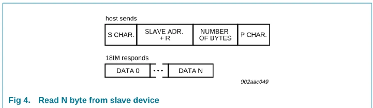
7.1.2 Read N byte from slave device
The host issues the read command by sending an S character followed by an I2C-bus
slave device address, and the total number of bytes to be read from the addressed I2C-bus slave. The frame is then terminated with a P character. Once the host issues this
command, the SC18IM700 will access the I2C-bus slave device, get the correct number of
bytes from the addressed I2C-bus slave, and then return the data to the host.
Note that the second byte sent is the I2C-bus device slave address. The least significant
bit (R) of this byte must be set to 1 to indicate this is an I2C-bus write command.
7.1.3 Write to 18IM internal register
The host issues the internal register write command by sending a W character followed by the register and data pair. Each register to be written must be followed by the data byte. The frame is then terminated with a P character.
Remark: Write and read from the internal 18IM register is processed immediately as soon
as the intended register is determined by 18IM. Fig 3. Write N bytes to slave device
002aac048 NUMBER
OF BYTES S CHAR. SLAVE ADR.
+ W host sends
DATA 0 DATA N P CHAR.
Fig 4. Read N byte from slave device
002aac049 NUMBER
OF BYTES S CHAR. SLAVE ADR.
+ R host sends
18IM responds
P CHAR.
DATA 0 DATA N
Fig 5. Write to 18IM internal register
002aac050 W CHAR. REGISTER 0 DATA 0 REGISTER N DATA N P CHAR.
7.1.4 Read from 18IM internal register
The host issues the internal register read command by sending an R character followed by the registers to be read. The frame is then terminated with a P character.
Once the command is issued, SC18IM700 will access its internal registers and returns the contents of these registers to the host.
7.1.5 Write to GPIO port
The host issues the output port write command by sending an O character followed by the data to be written to the output port. This command enables the host to quickly set any GPIO pins programmed as output without having to write to the SC18IM700 internal IOState register.
7.1.6 Read from GPIO port
The host issues the input port read command by sending an I character. This command enables the host to quickly read any GPIO pins programmed as input without having to read the SC18IM700 internal IOState register.
Once the command is issued, SC18IM700 will read its internal IOState register and returns its content to the host.
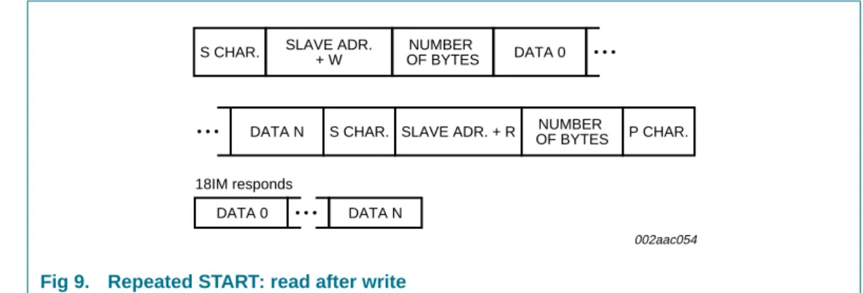
7.1.7 Repeated START: read after write
The SC18IM700 also supports ‘read after write’ command as specified in the NXP Semiconductors I2C-bus specification. This allows a read command to be sent after a
write command without having to issue a STOP condition between the two commands. The host issues a write command as normal, then immediately issues a read command without sending a STOP (P) character after the write command.
Fig 6. Read from 18IM internal register
002aac051 R CHAR. REGISTER 0 REGISTER N P CHAR.
18IM responds
DATA 0 DATA N
Fig 7. Write to output port
002aac052 O CHAR. DATA P CHAR.
Fig 8. Read from output port
002aac053 I CHAR.
18IM responds DATA
SC18IM700_2 © NXP B.V. 2007. All rights reserved.
Product data sheet Rev. 02 — 10 August 2007 7 of 22
NXP Semiconductors
SC18IM700
Master I2C-bus controller with UART interface
7.1.8 Repeated START: write after write
The SC18IM700 also supports ‘write after write’ command as specified in the NXP Semiconductors I2C-bus specification. This allows a write command to be sent after a
write command without having to issue a STOP condition between the two commands. The host issues a write command as normal, then immediately issues a second write command without sending a STOP (P) character after the first write command.
7.1.9 Power-down mode
The SC18IM700 can be placed in a low-power mode. In this mode the internal oscillator is stopped and SC18IM700 will no longer respond to the host messages. Enter the
Power-down mode by sending the power-down character Z (0x5A) followed by the two defined bytes, which are 0x5A and followed by 0xA5. If the exact message is not received, the device will not enter the power-down state.
Upon entering the power-down state, SC18IM700 places the WAKEUP pin in a HIGH state. To have the device leave the power-down state, the WAKEUP pin should be brought LOW. A 1 kΩ resistor must be connected between the WAKEUP pin and VDD.
Fig 9. Repeated START: read after write
002aac054 NUMBER
OF BYTES S CHAR. SLAVE ADR.+ W
S CHAR. NUMBER OF BYTES SLAVE ADR. + R DATA 0 DATA N P CHAR. 18IM responds DATA 0 DATA N
Fig 10. Repeated START: write after write
002aac055 NUMBER
OF BYTES S CHAR. SLAVE ADR.+ W
S CHAR. NUMBER
OF BYTES
SLAVE ADR. + W DATA 0 DATA 0
DATA N DATA N P CHAR.
Fig 11. Power-down mode
002aac056 Z CHAR. 0x5A 0xA5 P CHAR.
8.
I
2C-bus serial interface
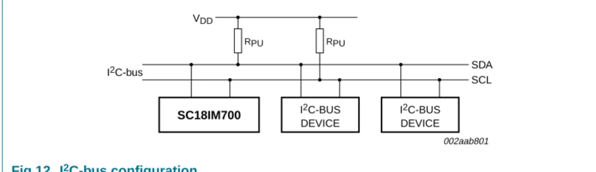
The I2C-bus uses two wires (SDA and SCL) to transfer information between devices
connected to the bus, and it has the following features:
•
Bidirectional data transfer between masters and slaves•
Multi-master bus (no central master)•
Arbitration between simultaneously transmitting masters without corruption of serial data on the bus•
Serial clock synchronization allows devices with different bit rates to communicate via one serial bus•
Serial clock synchronization can be used as a handshake mechanism to suspend and resume serial transfer.A typical I2C-bus configuration is shown inFigure 12. The SC18IM700 device provides a
byte-oriented I2C-bus interface that supports data transfers up to 400 kHz.
Fig 12. I2C-bus configuration
RPU 002aab801 VDD SC18IM700 I2C-BUS DEVICE I2C-BUS DEVICE I2C-bus SDA SCL RPU
xxxx xxxxxxxxxxxxxxxxxxxxxxxxxxxxxx x xxxxxxxxxxxxxx xxxxxxxxxx xxx xxxxxx xxxxxxxxxxxxxxxxxxxxxxx xxxxxxxxxxxxxxxxxxxxxx xxxxx xxxxxx xx xxxxxxxxxxxxxxxxxxxxxxxxxxxxx xxxxxxxxxxxxxxxxxxxxxx xxxxxxxxxxx xxxxxxx xxxxxxxxxxxxxxxxxxx xxxxxxxxxxxxxxxx xxxxxxxxxxxxxx xxxxxx xx xxxxxxxxxxxxxxxxxxxxxxxxxxxxxxxx xxxxxxxxxxxxxxxxxxxxxxxx xxxxxxx xxxxxxxxxxxxxxxxxxxxxxxxxxxxxxxxxxxxxxxxxxxxxx xxxxxxxxxxx xxxxx x x SC18IM700_2 © NXP B .V . 2007. All r ights reser v ed. Pr
oduct data sheet
Re v . 02 — 10 A ugust 2007 9 of 22
NXP Semiconductor
s
SC18IM700
Master I 2 C-b us contr oller with U A R T interface9.
Internal register
s a
v
ailab
le
9.1 Register summary
Table 4. Internal registers summary
Register address
Register Bit 7 Bit 6 Bit 5 Bit 4 Bit 3 Bit 2 Bit 1 Bit 0 R/W Default
value
General register set
0x00 BRG0 bit 7 bit 6 bit 5 bit 4 bit 3 bit 2 bit 1 bit 0 R/W 0xF0
0x01 BRG1 bit 7 bit 6 bit 5 bit 4 bit 3 bit 2 bit 1 bit 0 R/W 0x02
0x02 PortConf1 GPIO3.1 GPIO3.0 GPIO2.1 GPIO2.0 GPIO1.1 GPIO1.0 GPIO0.1 GPIO0.0 R/W 0x55
0x03 PortConf2 GPIO7.1 GPIO7.0 GPIO6.1 GPIO6.0 GPIO5.1 GPIO5.0 GPIO4.1 GPIO4.0 R/W 0x55
0x04 IOState GPIO7 GPIO6 GPIO5 GPIO4 GPIO3 GPIO2 GPIO1 GPIO0 R/W 0x0F
0x05 reserved bit 7 bit 6 bit 5 bit 4 bit 3 bit 2 bit 1 bit 0 - 0x00
0x06 I2CAdr bit 7 bit 6 bit 5 bit 4 bit 3 bit 2 bit 1 bit 0 R/W 0x26
0x07 I2CClkL bit 7 bit 6 bit 5 bit 4 bit 3 bit 2 bit 1 bit 0 R/W 0x13
0x08 I2CClkH bit 7 bit 6 bit 5 bit 4 bit 3 bit 2 bit 1 bit 0 R/W 0x13
0x09 I2CTO TO7 TO6 TO5 TO4 TO3 TO2 TO1 TE R/W 0x66
9.2 Register descriptions
9.2.1 Baud Rate Generator (BRG)The baud rate generator is an 8-bit counter that generates the data rate for the transmitter and the receiver. The rate is programmed through the BRG register and the baud rate can be calculated as follows:
Remark: To calculate the baud rate the values in the BRG registers must first be
converted from hex to decimal.
Remark: For the new baud rate to take effect, both BRG0 and BRG1 must be written in
sequence (BRG0, BRG1) with new values. The new baud rate will be in effect once BRG1 is written.
9.2.2 Programmable port configuration (PortConf1 and PortConf2)
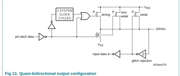
GPIO port 0 to port 7 may be configured by software to one of four types. These are: quasi-bidirectional, push-pull, open-drain, and input-only. Two bits are used to select the desired configuration for each port pin. PortConf1 is used to select the configuration for GPIO3 to GPIO0, and PortConf2 is used to select the configuration for GPIO7 to GPIO4. A port pin has Schmitt triggered input that also has a glitch suppression circuit.
9.2.2.1 Quasi-bidirectional output configuration
Quasi-bidirectional output type can be used as both an input and output without the need to reconfigure the port. This is possible because when the port outputs a logic HIGH, it is weakly driven, allowing an external device to pull the pin LOW. When the pin is driven LOW, it is driven strongly and able to sink a fairly large current. These features are somewhat similar to an open-drain output except that there are three pull-up transistors in the quasi-bidirectional output that serve different purposes.
The SC18IM700 is a 3 V device, but the pins are 5 V tolerant. In quasi-bidirectional mode, if a user applies 5 V on the pin, there will be a current flowing from the pin to VDD, causing
extra power consumption. Therefore, applying 5 V in quasi-bidirectional mode is discouraged.
A quasi-bidirectional port pin has a Schmitt triggered input that also has a glitch suppression circuit. Baud rate 7.3728 10 6 × 16+(BRG1 BRG0, ) ---=
Table 5. Port configurations
GPIOx.1 GPIOx.0 Port configuration
0 0 quasi-bidirectional output configuration 0 1 input-only configuration
1 0 push-pull output configuration 1 1 open-drain output configuration
SC18IM700_2 © NXP B.V. 2007. All rights reserved.
Product data sheet Rev. 02 — 10 August 2007 11 of 22
NXP Semiconductors
SC18IM700
Master I2C-bus controller with UART interface
9.2.2.2 Input-only configuration
The input-only port configuration has no output drivers. It is a Schmitt triggered input that also has a glitch suppression circuit.
9.2.2.3 Push-pull output configuration
The push-pull output configuration has the same pull-down structure as both the open-drain and the quasi-bidirectional output modes, but provides a continuous strong pull-up when the port latch contains a logic 1. The push-pull mode may be used when more source current is needed from a port output. A push-pull port pin has a Schmitt triggered input that also has a glitch suppression circuit.
Fig 13. Quasi-bidirectional output configuration
002aac076
2 SYSTEM CLOCK CYCLES
weak strong veryweak
VDD
P P P
VSS pin latch data
GPIOn
glitch rejection input data
Fig 14. Input-only configuration
002aab884 GPIO pin glitch rejection
input data
Fig 15. Push-pull output configuration
002aab885 strong
VDD P
VSS pin latch data
GPIO pin
glitch rejection input data
9.2.2.4 Open-drain output configuration
The open-drain output configuration turns off all pull-ups and only drives the pull-down transistor of the port driver when the port latch contains a logic 0. To be used as a logic output, a port configured in this manner must have an external pull-up, typically a resistor tied to VDD.
An open-drain port pin has a Schmitt triggered input that also has a glitch suppression circuit.
9.2.3 Programmable I/O pins state register (IOState)
When read, this register returns the actual state of all I/O pins. When written, each register bit will be transferred to the corresponding I/O pin programmed as output.
9.2.4 I2C-bus address register (I2CAdr)
The contents of the register represents the device’s own I2C-bus address. The most
significant bit corresponds to the first bit received from the I2C-bus after a START
condition. A logic 1 in I2CAdr corresponds to a HIGH level on the I2C-bus, and a logic 0
corresponds to a LOW level on the I2C-bus. The least significant bit is not used, but should
be programmed with a ‘0’.
I2CAdr is not needed for device operation, but should be configured so that its address does not conflict with an I2C-bus device address used by the bus master.
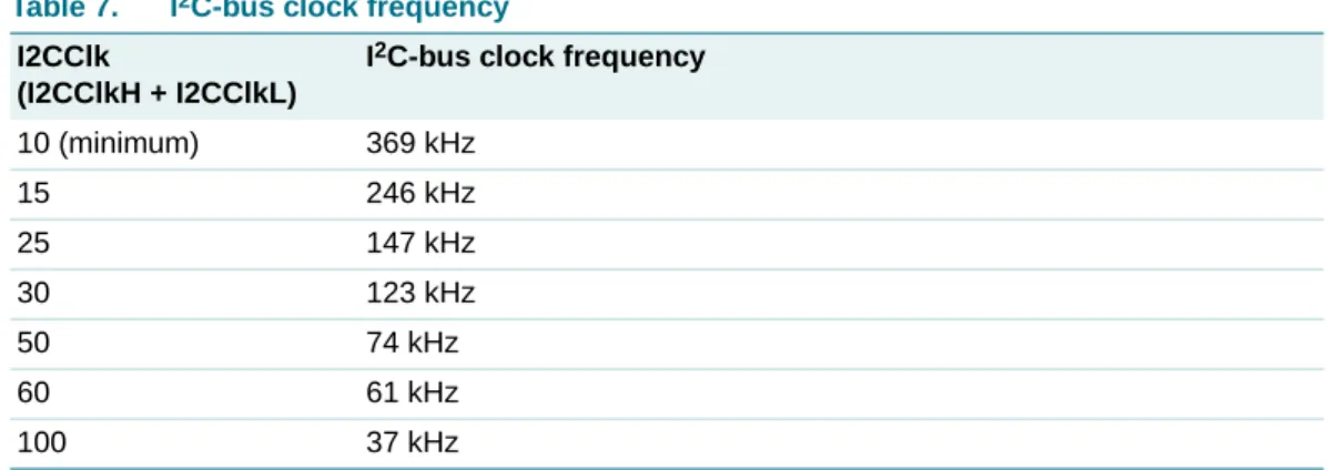
9.2.5 I2C-bus clock rates (I2CClk)
This register determines the serial clock frequency. The various serial rates are shown in
Table 7. The frequency can be determined using the following formula:
I2CClkH determines the SCL HIGH period, and I2CClkL determines the SCL LOW period. Fig 16. Open-drain output configuration
002aab883 VSS
pin latch data
GPIO pin
glitch rejection input data
Table 6. IOState - Programmable I/O pins state register (address 0x04h) bit description
Bit Symbol Description
7:0 IOLevel Set the logic level on the output pins. Write to this register:
logic 0 = set output pin to zero logic 1 = set output pin to one
Read this register returns states of all pins.
bit frequency 7.3728 10 6 × 2×(I 2CClkH+I 2CClkL) ---=
SC18IM700_2 © NXP B.V. 2007. All rights reserved.
Product data sheet Rev. 02 — 10 August 2007 13 of 22
NXP Semiconductors
SC18IM700
Master I2C-bus controller with UART interface
Remark: The numbers used in the formulas are in decimal, but the numbers to program
I2CClkH and I2CClkL are in hex. 9.2.6 I2C-bus time-out (I2CTO)
The time-out register is used to determine the maximum time that SCL is allowed to be LOW before the I2C-bus state machine is reset.
When the I2C-bus interface is running, I2CTO is loaded after each I2C-bus state transition.
The least significant bit of I2CTO (TE bit) is used as a time-out enable/disable. A logic 1 will enable the time-out function. The time-out period can be calculated as follows:
The time-out value may vary, and it is an approximate value. 9.2.7 I2C-bus status register (I2CStat)
This register reports the I2C-bus transmit and receive frame status, whether the frame
transmits correctly or not.
Table 7. I2C-bus clock frequency
I2CClk
(I2CClkH + I2CClkL)
I2C-bus clock frequency
10 (minimum) 369 kHz 15 246 kHz 25 147 kHz 30 123 kHz 50 74 kHz 60 61 kHz 100 37 kHz
Table 8. I2CTO - I2C-bus time-out register (address 0x09h) bit description
Bit Symbol Description
7:1 TO[7:1] time-out value
0 TE enable/disable time-out function logic 0 = disable
logic 1 = enable
time-out period I 2CTO 7:1[ ]×256 57600
--- seconds
=
Table 9. I2C-bus status
Bit 7 Bit 6 Bit 5 Bit 4 Bit 3 Bit 2 Bit 1 Bit 0 I2C-bus status description
1 1 1 1 0 0 0 0 I2C_OK
1 1 1 1 0 0 0 1 I2C_NACK_ON_ADDRESS
1 1 1 1 0 0 1 0 I2C_NACK_ON_DATA
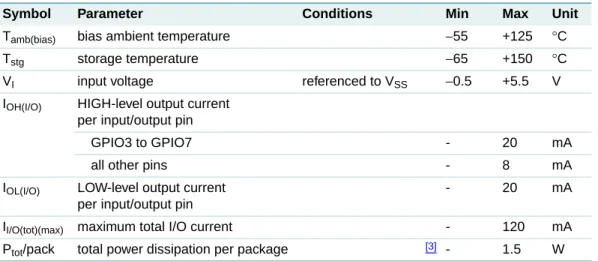
10. Limiting values
[1] This product includes circuitry specifically designed for the protection of its internal devices from the damaging effects of excessive static charge. Nonetheless, it is suggested that conventional precautions be taken to avoid applying greater than the rated maximum.
[2] Parameters are valid over operating temperature range unless otherwise specified. All voltages are with respect to VSS unless otherwise noted.
[3] Based on package heat transfer, not device power consumption.
Table 10. Limiting values
In accordance with the Absolute Maximum Rating System (IEC 60134).[1][2]
Symbol Parameter Conditions Min Max Unit
Tamb(bias) bias ambient temperature −55 +125 °C
Tstg storage temperature −65 +150 °C
VI input voltage referenced to VSS −0.5 +5.5 V
IOH(I/O) HIGH-level output current per input/output pin
GPIO3 to GPIO7 - 20 mA
all other pins - 8 mA
IOL(I/O) LOW-level output current per input/output pin
- 20 mA
II/O(tot)(max) maximum total I/O current - 120 mA Ptot/pack total power dissipation per package [3] - 1.5 W
SC18IM700_2 © NXP B.V. 2007. All rights reserved.
Product data sheet Rev. 02 — 10 August 2007 15 of 22
NXP Semiconductors
SC18IM700
Master I2C-bus controller with UART interface
11. Static characteristics
[1] Typical ratings are not guaranteed. The values listed are at room temperature, 3 V.
[2] SeeTable 10 “Limiting values” for steady state (non-transient) limits on IOL or IOH. If IOL/IOH exceeds the test condition, VOL/VOH may
exceed the related specification.
[3] Pin capacitance is characterized but not tested. [4] Measured with GPIO in quasi-bidirectional mode. [5] Measured with GPIO in high-impedance mode.
[6] GPIO in quasi-bidirectional mode with weak pull-up (applies to all GPIO pins with pull-ups). Does not apply to open-drain pins. [7] GPIO pins source a transition current when used in quasi-bidirectional mode and externally driven from logic 1 to logic 0. This current is
highest when VI is approximately 2 V. Table 11. Static characteristics
VDD= 2.4 V to 3.6 V; Tamb=−40°C to +85°C; unless otherwise specified.
Symbol Parameter Conditions Min Typ[1] Max Unit
IDD supply current VDD= 3.6 V
Operating mode; f = 7.3728 MHz - 9 15 mA
Idle mode; f = 7.3728 MHz - 3.25 5 mA
Power-down mode (sleep); GPIO0 to GPIO7 as inputs; inputs at VDD
- 50 70 µA
VPOR power-on reset voltage - - 0.2 V
Vth(HL) negative-going threshold voltage
except SCL, SDA 0.22VDD 0.4VDD - V
VIL LOW-level input voltage SCL, SDA only −0.5 - 0.3VDD V
Vth(LH) positive-going threshold voltage
except SCL, SDA - 0.6VDD 0.7VDD V
VIH HIGH-level input voltage SCL, SDA only 0.7VDD - 5.5 V
VOL LOW-level output voltage IOL= 20 mA [2] - 0.6 1.0 V IOL= 3.2 mA [2] - 0.2 0.3 V VOH HIGH-level output voltage
IOH=−20 mA; Push-pull mode; GPIO3 to GPIO7
0.8VDD - - V
IOH=−3.2 mA; Push-pull mode; GPIO0 to GPIO2
VDD−0.7 VDD−0.4 - V IOH=−20 mA; quasi-bidirectional
mode; all GPIOs
VDD−0.3 VDD−0.2 - V
Cio input/output capacitance [3] - - 15 pF
IIL LOW-level input current logic 0; all ports; VI= 0.4 V [4] - - −80 µA
ILI input leakage current all ports; VI= VIL or VIH [5] - - −10 µA IT(HL) negative-going transition
current
logic 1-to-0; all ports; VI= 2.0 V at VDD= 3.6 V
[6][7] −30 - −450 µA
RRESET_N(int) internal pull-up resistance on pin RESET
12. Dynamic characteristics
Table 12. I2C-bus timing characteristics
All the timing limits are valid within the operating supply voltage and ambient temperature range; VDD= 2.4 V to 3.6 V; Tamb=−40°C to +85°C; and refer to VIL and VIHwith an input voltage of VSSto VDD.
Symbol Parameter Conditions Standard mode I2C-bus
Fast mode I2C-bus
Unit Min Max Min Max
fSCL SCL clock frequency 0 100 0 400 kHz
tBUF bus free time between a STOP and START condition
4.7 - 1.3 - µs
tHD;STA hold time (repeated) START condition 4.0 - 0.6 - µs
tSU;STA set-up time for a repeated START condition 4.7 - 0.6 - µs
tSU;STO set-up time for STOP condition 4.0 - 0.6 - µs
tHD;DAT data hold time 0 - 0 - ns
tVD;ACK data valid acknowledge time - 0.6 - 0.6 µs
tVD;DAT data valid time LOW-level - 0.6 - 0.6 µs
HIGH-level - 0.6 - 0.6 µs
tSU;DAT data set-up time 250 - 100 - ns
tLOW LOW period of the SCL clock 4.7 - 1.3 - µs
tHIGH HIGH period of the SCL clock 4.0 - 0.6 - µs
tf fall time of both SDA and SCL signals - 0.3 - 0.3 µs
tr rise time of both SDA and SCL signals - 1 - 0.3 µs
tSP pulse width of spikes that must be suppressed by the input filter
- 50 - 50 ns
Fig 17. I2C-bus timing
SDA SCL 002aab271 tf S Sr P S tHD;STA tLOW tr tSU;DAT tf tHD;DAT tHIGH tSU;STA tHD;STA tSP tSU;STO tr tBUF
SC18IM700_2 © NXP B.V. 2007. All rights reserved.
Product data sheet Rev. 02 — 10 August 2007 17 of 22
NXP Semiconductors
SC18IM700
Master I2C-bus controller with UART interface
13. Package outline
Fig 18. Package outline SOT403-1 (TSSOP16)
UNIT A1 A2 A3 bp c D(1) E(2) e HE L Lp Q v w y Z(1) θ
REFERENCES OUTLINE
VERSION
EUROPEAN
PROJECTION ISSUE DATE
IEC JEDEC JEITA
mm 0.15 0.05 0.95 0.80 0.30 0.19 0.2 0.1 5.1 4.9 4.5 4.3 0.65 6.6 6.2 0.4 0.3 0.40 0.06 8 0 o o 0.13 0.1 0.2 1
DIMENSIONS (mm are the original dimensions)
Notes
1. Plastic or metal protrusions of 0.15 mm maximum per side are not included. 2. Plastic interlead protrusions of 0.25 mm maximum per side are not included.
0.75 0.50 SOT403-1 MO-153 99-12-27 03-02-18 w M bp D Z e 0.25 1 8 16 9 θ A A1 A2 Lp Q detail X L (A )3 HE E c v M A X A y 0 2.5 5 mm scale
TSSOP16: plastic thin shrink small outline package; 16 leads; body width 4.4 mm SOT403-1
A max.
1.1
14. Soldering
This text provides a very brief insight into a complex technology. A more in-depth account of soldering ICs can be found in Application NoteAN10365 “Surface mount reflow soldering description”.
14.1 Introduction to soldering
Soldering is one of the most common methods through which packages are attached to Printed Circuit Boards (PCBs), to form electrical circuits. The soldered joint provides both the mechanical and the electrical connection. There is no single soldering method that is ideal for all IC packages. Wave soldering is often preferred when through-hole and Surface Mount Devices (SMDs) are mixed on one printed wiring board; however, it is not suitable for fine pitch SMDs. Reflow soldering is ideal for the small pitches and high densities that come with increased miniaturization.
14.2 Wave and reflow soldering
Wave soldering is a joining technology in which the joints are made by solder coming from a standing wave of liquid solder. The wave soldering process is suitable for the following:
•
Through-hole components•
Leaded or leadless SMDs, which are glued to the surface of the printed circuit board Not all SMDs can be wave soldered. Packages with solder balls, and some leadless packages which have solder lands underneath the body, cannot be wave soldered. Also, leaded SMDs with leads having a pitch smaller than ~0.6 mm cannot be wave soldered, due to an increased probability of bridging.The reflow soldering process involves applying solder paste to a board, followed by component placement and exposure to a temperature profile. Leaded packages, packages with solder balls, and leadless packages are all reflow solderable. Key characteristics in both wave and reflow soldering are:
•
Board specifications, including the board finish, solder masks and vias•
Package footprints, including solder thieves and orientation•
The moisture sensitivity level of the packages•
Package placement•
Inspection and repair•
Lead-free soldering versus PbSn soldering14.3 Wave soldering
Key characteristics in wave soldering are:
•
Process issues, such as application of adhesive and flux, clinching of leads, board transport, the solder wave parameters, and the time during which components are exposed to the waveSC18IM700_2 © NXP B.V. 2007. All rights reserved.
Product data sheet Rev. 02 — 10 August 2007 19 of 22
NXP Semiconductors
SC18IM700
Master I2C-bus controller with UART interface
14.4 Reflow soldering
Key characteristics in reflow soldering are:
•
Lead-free versus SnPb soldering; note that a lead-free reflow process usually leads to higher minimum peak temperatures (seeFigure 19) than a PbSn process, thus reducing the process window•
Solder paste printing issues including smearing, release, and adjusting the process window for a mix of large and small components on one board•
Reflow temperature profile; this profile includes preheat, reflow (in which the board is heated to the peak temperature) and cooling down. It is imperative that the peak temperature is high enough for the solder to make reliable solder joints (a solder paste characteristic). In addition, the peak temperature must be low enough that the packages and/or boards are not damaged. The peak temperature of the package depends on package thickness and volume and is classified in accordance withTable 13 and14
Moisture sensitivity precautions, as indicated on the packing, must be respected at all times.
Studies have shown that small packages reach higher temperatures during reflow soldering, seeFigure 19.
Table 13. SnPb eutectic process (from J-STD-020C)
Package thickness (mm) Package reflow temperature (°C) Volume (mm3)
< 350 ≥ 350
< 2.5 235 220
≥ 2.5 220 220
Table 14. Lead-free process (from J-STD-020C)
Package thickness (mm) Package reflow temperature (°C) Volume (mm3)
< 350 350 to 2000 > 2000
< 1.6 260 260 260
1.6 to 2.5 260 250 245
For further information on temperature profiles, refer to Application NoteAN10365 “Surface mount reflow soldering description”.
15. Abbreviations
16. Revision history
MSL: Moisture Sensitivity Level
Fig 19. Temperature profiles for large and small components
001aac844 temperature
time
minimum peak temperature = minimum soldering temperature
maximum peak temperature = MSL limit, damage level
peak temperature
Table 15. Abbreviations
Acronym Description
ASCII American Standard Code for Information Interchange FIFO First In, First Out
GPIO General Purpose Input/Output I2C-bus Inter Integrated Circuit bus RX FIFO Receive FIFO
TX FIFO Transmit FIFO
UART Universal Asynchronous Receiver/Transmitter
Table 16. Revision history
Document ID Release date Data sheet status Change notice Supersedes
SC18IM700_2 20070810 Product data sheet - SC18IM700_1
Modifications:
•
The format of this data sheet has been redesigned to comply with the new identity guidelines of NXP Semiconductors.•
Legal texts have been adapted to the new company name where appropriate.•
Table 4 “Internal registers summary”: added column “Default value”-SC18IM700_2 © NXP B.V. 2007. All rights reserved.
Product data sheet Rev. 02 — 10 August 2007 21 of 22
NXP Semiconductors
SC18IM700
Master I2C-bus controller with UART interface
17. Legal information
17.1
Data sheet status
[1] Please consult the most recently issued document before initiating or completing a design. [2] The term ‘short data sheet’ is explained in section “Definitions”.
[3] The product status of device(s) described in this document may have changed since this document was published and may differ in case of multiple devices. The latest product status information is available on the Internet at URLhttp://www.nxp.com.
17.2
Definitions
Draft — The document is a draft version only. The content is still under
internal review and subject to formal approval, which may result in modifications or additions. NXP Semiconductors does not give any representations or warranties as to the accuracy or completeness of information included herein and shall have no liability for the consequences of use of such information.
Short data sheet — A short data sheet is an extract from a full data sheet
with the same product type number(s) and title. A short data sheet is intended for quick reference only and should not be relied upon to contain detailed and full information. For detailed and full information see the relevant full data sheet, which is available on request via the local NXP Semiconductors sales office. In case of any inconsistency or conflict with the short data sheet, the full data sheet shall prevail.
17.3
Disclaimers
General — Information in this document is believed to be accurate and
reliable. However, NXP Semiconductors does not give any representations or warranties, expressed or implied, as to the accuracy or completeness of such information and shall have no liability for the consequences of use of such information.
Right to make changes — NXP Semiconductors reserves the right to make
changes to information published in this document, including without limitation specifications and product descriptions, at any time and without notice. This document supersedes and replaces all information supplied prior to the publication hereof.
Suitability for use — NXP Semiconductors products are not designed,
authorized or warranted to be suitable for use in medical, military, aircraft, space or life support equipment, nor in applications where failure or malfunction of a NXP Semiconductors product can reasonably be expected to
result in personal injury, death or severe property or environmental damage. NXP Semiconductors accepts no liability for inclusion and/or use of NXP Semiconductors products in such equipment or applications and therefore such inclusion and/or use is at the customer’s own risk.
Applications — Applications that are described herein for any of these
products are for illustrative purposes only. NXP Semiconductors makes no representation or warranty that such applications will be suitable for the specified use without further testing or modification.
Limiting values — Stress above one or more limiting values (as defined in
the Absolute Maximum Ratings System of IEC 60134) may cause permanent damage to the device. Limiting values are stress ratings only and operation of the device at these or any other conditions above those given in the Characteristics sections of this document is not implied. Exposure to limiting values for extended periods may affect device reliability.
Terms and conditions of sale — NXP Semiconductors products are sold
subject to the general terms and conditions of commercial sale, as published athttp://www.nxp.com/profile/terms, including those pertaining to warranty, intellectual property rights infringement and limitation of liability, unless explicitly otherwise agreed to in writing by NXP Semiconductors. In case of any inconsistency or conflict between information in this document and such terms and conditions, the latter will prevail.
No offer to sell or license — Nothing in this document may be interpreted
or construed as an offer to sell products that is open for acceptance or the grant, conveyance or implication of any license under any copyrights, patents or other industrial or intellectual property rights.
17.4
Trademarks
Notice: All referenced brands, product names, service names and trademarks are the property of their respective owners.
I2C-bus — logo is a trademark of NXP B.V.
18. Contact information
For additional information, please visit:http://www.nxp.com
For sales office addresses, send an email to:[email protected] Document status[1][2] Product status[3] Definition
Objective [short] data sheet Development This document contains data from the objective specification for product development. Preliminary [short] data sheet Qualification This document contains data from the preliminary specification.
© NXP B.V. 2007. All rights reserved.
For more information, please visit: http://www.nxp.com
For sales office addresses, please send an email to: [email protected] Date of release: 10 August 2007 Please be aware that important notices concerning this document and the product(s) described herein, have been included in section ‘Legal information’.
19. Contents
1 General description . . . 1 2 Features . . . 1 3 Applications . . . 1 4 Ordering information . . . 2 5 Block diagram . . . 2 6 Pinning information . . . 3 6.1 Pinning . . . 3 6.2 Pin description . . . 3 7 Functional description . . . 47.1 UART message format . . . 4
7.1.1 Write N bytes to slave device . . . 4
7.1.2 Read N byte from slave device . . . 5
7.1.3 Write to 18IM internal register . . . 5
7.1.4 Read from 18IM internal register . . . 6
7.1.5 Write to GPIO port . . . 6
7.1.6 Read from GPIO port . . . 6
7.1.7 Repeated START: read after write . . . 6
7.1.8 Repeated START: write after write . . . 7
7.1.9 Power-down mode . . . 7
8 I2C-bus serial interface . . . 8
9 Internal registers available . . . 9
9.1 Register summary . . . 9
9.2 Register descriptions . . . 10
9.2.1 Baud Rate Generator (BRG) . . . 10
9.2.2 Programmable port configuration (PortConf1 and PortConf2) . . . 10
9.2.2.1 Quasi-bidirectional output configuration . . . 10
9.2.2.2 Input-only configuration . . . 11
9.2.2.3 Push-pull output configuration . . . 11
9.2.2.4 Open-drain output configuration . . . 12
9.2.3 Programmable I/O pins state register (IOState) . . . 12
9.2.4 I2C-bus address register (I2CAdr) . . . 12
9.2.5 I2C-bus clock rates (I2CClk) . . . 12
9.2.6 I2C-bus time-out (I2CTO) . . . 13
9.2.7 I2C-bus status register (I2CStat). . . 13
10 Limiting values. . . 14 11 Static characteristics. . . 15 12 Dynamic characteristics . . . 16 13 Package outline . . . 17 14 Soldering . . . 18 14.1 Introduction to soldering . . . 18
14.2 Wave and reflow soldering . . . 18
14.3 Wave soldering . . . 18
14.4 Reflow soldering . . . 19
15 Abbreviations . . . 20
16 Revision history . . . 20
17 Legal information . . . 21
17.1 Data sheet status . . . 21
17.2 Definitions . . . 21
17.3 Disclaimers. . . 21
17.4 Trademarks . . . 21
18 Contact information . . . 21