© 2017, IRJET | Impact Factor value: 5.181 | ISO 9001:2008 Certified Journal
| Page 343
Review of MEMS technology & its applications in various fields
Prof. Ms. D. S. Bhade
Assistant Professor
DMIETR, Wardha, Maharashtra
---***---
Abstract
- MEMS are small integrated devices whichcombine electronics, electrical as well as mechanical element to meet the control related functional requirements such as sensing and actuation. Basically MEMS technology believes in Good things comes in small packet. To satisfy today’s market demand miniaturization is the only solution. The miniaturized devices are particularly suited for biomedical & aerospace application due to their minute size & weight. MEMS devices are consider to range in characteristic length from one millimeter down to one micron-many times smaller than the diameter of a human hair. MEMS are the integration of active and passive element on a single silicon substrate developed through more advanced IC processing technology. MEMS consist of mechanical microstructures, micro sensors, micro actuators and microelectronics, all integrated onto the same silicon chip. Almost every smart phone is now equipped with a MEMS accelerometer-gyroscope system. The core element in MEMS generally consists of two principal components, sensing or actuating element and a signal transduction unit. There are different micro sensors developed for various application and widely used in the society. Some of the common sensors are biosensor, chemical sensor, optical sensors, thermal & pressure sensors. The application of Micro Electro Mechanical Systems (MEMS) in the biomedical field is leading to a new generation of medical devices. In this paper we will discuss MEMS technology and its applications in various fields. Biomedical sensor and biosensor used for diagnostic analyses. These sensors require a minute amount of sample and can produce results significantly faster than the traditional biomedical instrument, the cost of these biosensors are low as they produced in batches and easily disposable after use. There are many other types of micro sensors that are available in the market. They include chemical sensors for detecting chemicals or toxic gases such as CO, CO2, NO, O3, and NH3 etc.
Keywords-MEMS, Micro sensor, Micro actuator, Micro
fabrication
1.
INTRODUCTION
Microsystem Technology based on the advancement made in development of IC fabrication process. MEMS technology smartly integrate electronics, electrical &
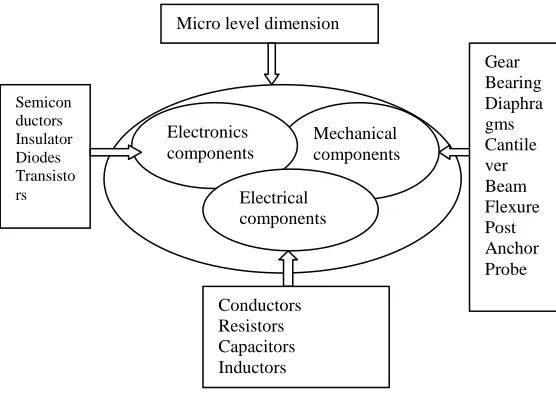
Mechanical components on a single silicon wafer similar to integrated circuit technology. We can say that MEMS is the integration of active elements that is sensors, actuators and passive electronics as well as mechanical system as sown in figure 1.In IC fabrication technology, fabrication of 3D mechanical components such as plate, beam, cantilever, diaphragm, gear etc. as well as electrical components such as inductors & capacitors are not possible, whereas MEMS technology adapted modified micromachining techniques to fabricate these devices. This makes it possible for MEMS technology to realize system-on-a-chip design.
Fig-1: MEMS Devices [2]
It combines microelectronic, micromechanics & micro optics. MEMS have been identified as one of the most promising technologies for this century and have the capacity to combine both industrial and consumer products by
combining silicon based microelectronics with
micromachining technology. This emerging technique has the tremendous power to affect all our life.
Micro level dimension
Mechanical components Electronics
components
Electrical components
Semicon ductors Insulator Diodes Transisto rs
Conductors Resistors Capacitors Inductors
[image:1.612.308.586.319.523.2]© 2017, IRJET | Impact Factor value: 5.181 | ISO 9001:2008 Certified Journal
| Page 344
Fig-2: Components of Microsystems
2. MICRO SENSORS & MICROACTUATORS
2.1 Microsensors
Sensor is a device that converts one form of energy into another which gives output in response to specific measurable input. A sensor system includes the sensing element and related signal processing hardware. The signal processing circuit could be an amplifier, analog to digital converter, an offset compensator etc. Sensors which are designed by using MEMS technology are called micro machined micro sensors or MEMS sensors. Sensors are classified into different types depending on the nature of signal they handle, selective material of the transducer, and the level of signal generation. Now we will discuss some of the commonly used MEMS sensor
i) Silicon Capacitive Accelerometer: It measures the acceleration of the body on which it is mounted .It converts the displacement caused by the inertial force on the proof mass to a voltage signal via change in capacitance between movable and fixed parts. It is mainly used in Automotive
ii) Pressure sensors: These sensors function on the principle of mechanical deformation and stresses of thin diaphragms induced by the pressure. This deformation then converted into electrical signal output with the help of transduction unit. Pressure sensor mainly used in Flow sensing application, Automobile, biomedical application, aerospace, direct pressure sensing application etc.
iii) Optical sensors: These optical sensors convert optical signal into electronic output. Micro-optical sensors have been developed to sense the intensity of light. The mostly used optical sensors are photovoltaic junction,
photoconductive devices, photodiodes, and
phototransistors. All these devices convert incident photon energy into electric output. Semiconducting material such as silicon (Si), gallium arsenide (GaAs) are common materials used for optical sensors.
iv) Thermal sensors: A thermocouple is a transducer used for the measurement of temperature. It consists of two dissimilar metals, joined together at one end, called thermocouple junction. When the temperature of this junction is different from the temperature of other parts of the metal an EMF is generated.
v) Chemical sensors: These sensors are used to sense particular chemical compounds, such as various gas species. We know that many materials are sensitive to chemical attacks and this property of material is the basis for many chemical sensors.
vi) BioMEMS: In Biomedicine two types of sensors are mostly used that is biomedical sensors and Biosensors. Biomedical sensors are used to detect biological substances, whereas biosensors are the measuring devices that contain biological element. These sensors usually involve biological molecules such as antibodies or enzymes, which interact with analyses that are to be detected. To design and manufactures this biomems one require the knowledge & experience in molecular biology as well as physical chemistry in addition to engineering. The manufacturer has to think about biological system of patient as well as about its mobility & easy navigation for operations.
2.2
Micro actuators
The actuator is a very important part of a microsystem that involves motion .The process of micro movement is called micro actuation. Micro actuators are lightweight, conformable and precision devices. The commonly available micro actuators are Mechanical actuators, Electrostatic actuators, Thermal actuators and Magnetic actuators. Electrostatic actuation is widely used in devices and machines at micro scales. The micro actuations applications are:
a) Actuation of micro mirrors to scan laser beams. b) Driving of cutting tools for microsurgical applications. c) Driving of micro pumps and valves for fluid &
gas transportation d) Printing application
e) Spatial light modulation for display application f) Optical signal switching
g) RF signal tuning
3. MICROFABRICATION PROCESS
Fabrication of microsystem is known as
micromachining..Materials used for micromachining are semiconductors, metals, ceramics, polymers etc. The most common substrate material for micromachining is silicon because of following reason
1. Silicon is abundant, inexpensive
2. Silicon’s ability to be deposited in thin films is very amenable to MEMS
Power Supply
Signal transduction &
processing uunitUnit
Sensor Actuator
© 2017, IRJET | Impact Factor value: 5.181 | ISO 9001:2008 Certified Journal
| Page 345
3. High definition and reproduction of silicon deviceshapes using photolithography are perfect for high levels of MEMS precision
4. Silicon has desirable electrical & mechanical properties required for micromachining.
MEMS devices have been fabricated using the well-known micromachining techniques used in the integrated circuit domain, such as: photolithography, thin film deposition by chemical vapor deposition (CVD) or physical vapor deposition (PVD), thin film growth by oxidation and epitaxy, doping by ion implantation or diffusion, wet etching, dry etching, etc. as shown in fig.3. MEMS devices have the potential of providing significant cost advantages when batch fabricated. The micromachining process can use the material to form microstructures by etching directly into the material or use structural layer. Most widely used micro fabrication processes are bulk micromachining and surface
micromachining.
Fig-3: Basic steps involved microelectronics fabrication
3.1Bulk Micromachining
: Most of the commercialmicrosystem devices are fabricated using bulk micromachining. It was first used in microelectronics in 1960s.In bulk micromachining technique, significant
amount of material is removed from silicon wafer to form membranes, cantilever beams, different types of trenches, holes and other types of structures. Now let’s see how to build cantilever beam on a silicon wafer by using Bulk Micromachining
i) Grow thick layer of silicon dioxide on silicon wafer.
ii) ii) Apply a layer of photoresist on silicon dioxide surface.
iii) Next is the photolithography process to define cantilever geometry.
iv) Etch out oxide in unwanted area to form cantilever beam and expose silicon surface.
v) Do anisotropic etching to form cavity in silicon wafer.
3.2 Surface Micromachining:
In contrast to BulkMicromachining, Surface Micromachining build
microstructures by adding material layer on the top of the substrate. Basic steps involved in Surface Micromachining are:
i) Deposition & patterning of sacrificial layer mostly silicon dioxide
ii) Deposition & patterning of structural (polysilicon) layer.
iii)Removal of sacrificial layer.
Fig- 4: Surface Micromaching process sequence Silicon wafer preparation
(substrate)
Thin film deposition by using PVD or CVD
Apply layer of photo resist on it
UV exposure under aligned mask
Desired pattern development as per mask
Etching (Remove the photoresist from exposed area)
Remove the photoresist from exposed area
Wafer preparation &
cleaning
Sacrificial layer deposition that is thin dielectric insulating layer
Base patterning with primary mask layer
Deposition of structural layer
Pattern microstructure with second mask layer
Selective etching of sacrificial layer
© 2017, IRJET | Impact Factor value: 5.181 | ISO 9001:2008 Certified Journal
| Page 346
Bulk Micromachining Surface Micromachining
Established 1960 1980
Process Maturity Well established Fairly well established
Ruggedness Structure can withstand vibration & shock
Less rugged
Die area Large Small
IC compatibility Not fully integrated IC compatible
Structure Geometry Limited option Wide range possible
Planar Geometry Rectangular Unrestricted
Comparison between Bulk & Surface Micromachining [3]
3.3 LIGA Process:
To overcome disadvantage of Bulk & Surface Micromachining that is low geometric aspect ratio, use of only silicon based material, LIGA process have been used..LIGA means Lithography (Electroforming & Molding)
Fig-5: LIGA process steps [3]
LIGA process is the most expensive micro fabrication process. The major advantages of LIGA process are, It is the best manufacturing process than others for mass production, with the provision for injection molding ,also it allows the production of metallic microstructures with unlimited aspect ratio of the microstructure geometry.
4. MICROSYSTEM PACKAGING
The purpose of microelectronics packaging is to provide mechanical support, electrical connections, and protection of the delicate integrated circuits from all possible attacks by mechanical and environmental sources. It also removed heat generated by the integrated circuits. The three levels of microsystem packaging are: Die level, Device level & System level packaging
Types of Microsystem Packages
i) Metal packages: Metal packages are often used for microwave integrated circuits and hybrid circuits because they provide excellent thermal dissipation and excellent electromagnetic shielding.
ii) Ceramic packages: This type of packaging is popular in microelectronics industry due to its low mass,low cost and ease of mass production.
Fig.6.Three levels of microsystem packaging[1]
iii)Plastic packages: This packages uses resin material to encapsulate chip. The packages are also susceptible to cracking in humid environments during temperature cycling This is most common type of packaging due to its low cost.
iv) Low-temperature co-fired ceramic packages (LTCC):
These are constructed from individual pieces of thick film sheets of ceramic& then metal lines are deposited in each film by thick processing.
5. APPLICATION OF MEMS
MEMS technology adapts miniaturization which makes them suitable for each & every application to makes a system smart one. As we know the miniaturized systems have better response time, faster analysis and diagnosis, Deep x-ray lithography
Desired patterns on thik photoresist
Electroplating of metal on patterns
Metal molds
Metal product
© 2017, IRJET | Impact Factor value: 5.181 | ISO 9001:2008 Certified Journal
| Page 347
less power consumption etc. Now we will discuss majorapplication of MEMS in some industry. A] In Automotive industry:
i) Inertial sensors have been used in Airbags and antilock braking system for safety purpose, vehicle
dynamic control, navigation systems.
Active suspension, roll detection
ii) Pressure sensors have been used in manifold air
iii) Pressure, tire pressure management systems.
iv) Flow sensors have been used to check air intake of Engine, air quality in cabin. Microphones have been used for hand free calling.
B] In Health Care Industry:
i) Intrauterine pressure sensors have been used to monitor pressure during child delivery. Also Angioplasty pressure sensors are used to monitor the pressure inside the balloon once it is inside the blood vessel.
ii) Optical sensors have been used in Micro
iii) spectrometers for patient self-testing and monitoring
iv) Microfluidic devices have been used for insulin pump & micro needles. C] In Telecommunication field
i) RF MEMS have been used in tunable
Capacitors and resonators for mobile phones, Switches in base stations.
ii) Optical sensors are used in Variable optical Attenuators, optical switching, tunable filters D] In consumer Product
i) IR sensors are used in Cabin temperature Control, crash prevention, anti-fog systems, seat Occupancy, tire and break monitoring system
ii) Microfluidic devices are used in inkjet heads
iii) Microphones have been used in Mobile phones, Note books, camcorder.
iv) Inertial sensors are used in Pedometer, game Control, image stabilization in video cameras, Hard disk protection
E] In Aerospace & Defense
i) RF MEMS have been used in Switches and
Tunable capacitors for radar and communications.
ii) Inertial sensors are used in Missile guidance, Navigation, laser range finder application
iii) Pressure sensors are used in Flight control Systems, cabin pressure monitoring, hydraulic Systems
iv) IR sensors are used for security monitoring
6. CONCLUSION
Miniaturization is the need of today’s world, as everything is digitized. Last few decades have shown the growth in microelectronics industry. The boom of microelctomechanical industry in recent years would not have been possible without the development of microelectronic system. .There is no doubt that for all future innovations in every walk of human endeavor, the rapid growth of MEMS technology plays a vital role. As per earlier discussion we can say the multidisciplinary mature of MEMS technology makes it suitable for each and every field that is automobile, medical, aerospace, telecommunication, consumer product etc.
Currently, MEMS market demands are strongly becoming high .This technology adapted new advanced micromachining process for fabrication of products that meet customer requirement as well as performance. In this paper we discuss the need of miniaturization, different sensors and actuators used in MEMS technology. Also this paper focuses on microfabrication process need to design MEMS structure. The various application of microsystem discussed in this paper clearly specify how MEMS technology becomes an integral part of each & every field.
REFERENCES
[1] “MEMS & MICROSYSTEMS Design and Manufacture” by Tai-Ran Hsu Mc Graw Hill Education
[2] MEMS by Nitaigour Premchand Mahalik Mc Graw Hill Education
[3] “MICRO AND SMART SYSTEMS” by
G.K.Ananthasuresh,K.J.Vinoy,S.Gopalakrishnan,K.N.Bhat, V.K.Atre Wiley India Pvt..Ltd..
[4] Nidhi Maheshwari, Gaurav Chatterjee,V. Ramgopal Rao “A Technology Overview and Applications of Bio-MEMS” J. ISSS Vol. 3 No. 2, pp. 39-59, Sept. 2014.
[5] Srinivasa Rao Karumuri.K.Girija Sravani, S. Durga Sailaja, J.Vijay Sekhar,Y.Srinivas, Ramendu Bhattacharje, “Micro-Electro-Mechanical-Systems (MEMS) Technology” Scholars Research Library Archives of Applied Science Research, 2012, 4 (1):307- 314
[6]N.Maluf,“AnIntroduction to Microelectromechanical Systems Engineering” Artech House, Norwood, MA, 2000