N e a r-I nf r a r e d a n d s h o r
t-w a v el e n g t h i nf r a r e d p h o t o di o d e s
b a s e d o n d y e-p e r o v s ki t e
c o m p o si t e s
M a r t i n e z M a e s t r o , L, Qi a n qi a n , L, Wa n g , Y, You n g , M , P a t e l, JB,
Milo t, RL, L u n t , RR, S n a i t h , HJ, Jo h n s t o n , M B a n d H e r z , LM
h t t p :// dx. d oi.o r g / 1 0 . 1 0 0 2 / a df m . 2 0 1 7 0 2 4 8 5
T i t l e
N e a r-I nf r a r e d a n d s h o r t-w a v el e n g t h inf r a r e d p h o t o di o d e s
b a s e d o n d y e-p e r o v s ki t e c o m p o si t e s
A u t h o r s
M a r ti n e z M a e s t r o , L, Qi a n qi a n , L, Wa n g , Y, You n g , M ,
P a t el, JB, Milo t, RL, L u n t , RR, S n a i t h , HJ, Jo h n s t o n , M B
a n d H e r z, LM
Typ e
Ar ticl e
U RL
T hi s v e r si o n is a v ail a bl e a t :
h t t p :// u sir. s alfo r d . a c . u k /i d/ e p ri n t/ 5 3 2 5 0 /
P u b l i s h e d D a t e
2 0 1 7
U S IR is a d i gi t al c oll e c ti o n of t h e r e s e a r c h o u t p u t of t h e U n iv e r si ty of S alfo r d .
W h e r e c o p y ri g h t p e r m i t s , f ull t e x t m a t e r i al h el d i n t h e r e p o si t o r y is m a d e
f r e ely a v ail a bl e o nli n e a n d c a n b e r e a d , d o w nl o a d e d a n d c o pi e d fo r n o
n-c o m m e r n-ci al p r iv a t e s t u d y o r r e s e a r n-c h p u r p o s e s . Pl e a s e n-c h e n-c k t h e m a n u s n-c ri p t
fo r a n y f u r t h e r c o p y ri g h t r e s t r i c ti o n s .
www.afm-journal.de
Near-Infrared and Short-Wavelength Infrared Photodiodes
Based on Dye–Perovskite Composites
Qianqian Lin, Zhiping Wang, Margaret Young, Jay B. Patel, Rebecca L. Milot,
Laura Martinez Maestro, Richard R. Lunt, Henry J. Snaith, Michael B. Johnston,
and Laura M. Herz*
Organohalide perovskites have emerged as promising light-sensing materials because of their superior optoelectronic properties and low-cost processing methods. Recently, perovskite-based photodetectors have successfully been demonstrated as both broadband and narrowband varieties. However, the photodetection bandwidth in perovskite-based photodetectors has so far been limited to the near-infrared regime owing to the relatively wide band gap of hybrid organohalide perovskites. In particular, short-wavelength infrared photodiodes operating beyond 1 µm have not yet been realized with organo-halide perovskites. In this study, narrow band gap organic dyes are combined with hybrid perovskites to form composite films as active photoresponsive layers. Tuning the dye loading allows for optimization of the spectral response characteristics and excellent charge-carrier mobilities near 11 cm2 V−1 s−1,
suggesting that these composites combine the light-absorbing properties or IR dyes with the outstanding charge-extraction characteristics of the pero-vskite. This study demonstrates the first perovskite photodiodes with deep near-infrared and short-wavelength infrared response that extends as far as 1.6 µm. All devices are solution-processed and exhibit relatively high respon-sivity, low dark current, and fast response at room temperature, making this approach highly attractive for next-generation light-detection techniques.
DOI: 10.1002/adfm.201702485
Dr. Q. Lin, Dr. Z. Wang, J. B. Patel, Dr. R. L. Milot, Dr. L. Martinez Maestro, Prof. H. J. Snaith, Prof. M. B. Johnston, Prof. L. M. Herz Clarendon Laboratory
University of Oxford
Parks Rd, Oxford OX1 3PU, UK E-mail: laura.herz@physics.ox.ac.uk M. Young, Prof. R. R. Lunt
Department of Chemical Engineering and Materials Science Michigan State University
East Lansing, MI 48824, USA
The ORCID identification number(s) for the author(s) of this article can be found under https://doi.org/10.1002/adfm.201702485.
photodetectors are based on crystalline inorganic semiconductors, such as Si, GaAs, GaP, Ge, PbS, and InGaAs.[2,4] In
particular, silicon is used for charge-coupled devices and sensors based on com-plementary metal–oxide–semiconductor technology, which dominate the current image-sensor market.[5] Silicon-based
detectors are also extensively used in spec-troscopy and advanced light detection sys-tems. However, the photoresponse of such detectors is normally limited by the band gap of the active material, which leads to a long-wavelength cut-off around 1.1 µm[6]
for silicon-based devices. As an alterna-tive, Ge, PbS, and InGaAs photodetectors have been introduced to allow detection of infrared light, albeit at substantially higher cost and cooling requirements to ensure high efficiency of photodetection. Hence, low-noise, efficient photodetectors with broad photoresponse covering the whole range of ultraviolet, visible, near-infrared (NIR, ≈0.75–1 µm), and short-wavelength infrared (SWIR, ≈1–3 µm) could play an important role in advancing light sensing.[7–9]
Recently, solution-processed organic semiconductors,[10–12]
quantum dots,[9,13,14] and organohalide perovskites (OHPs)[15–18]
have emerged as promising candidates for next generation photodetection, combining the merits of low fabrication costs, tailorable optoelectronic properties, and excellent perfor-mance.[3] Photodetectors based on organohalide perovskites,
in particular, have emerged over the last three years as a novel and highly promising technology, benefiting from the rapid progress in understanding of perovskite optoelectronics associ-ated with their use in photovoltaic cells.[19,20] Many new OHPs
combine the beneficial chemical properties of hybrid materials with extraordinary optoelectronic performance. Organic–inor-ganic lead halide perovskites can be easily solution-processed or thermally evaporated,[20,21] possess high electron and hole
mobilities[22] and long charge-carrier diffusion lengths and
lifetimes compared with other solution-processable semicon-ductors, allow for band-gap tuning through simple chemical substitutions, and are compatible with flexible platforms.[23,24]
This collection of properties offers substantial benefits to the device performance of an OHP-based photo detector. For instance, high charge-carrier mobilities will result in a fast photoresponse; the tunable band gap allows control over
Photodiodes
1. Introduction
The detection of light underpins modern science and tech-nology, including imaging, surveillance, communication, bio-logical sensing, and machine vision.[1–3] Most commercial
www.afm-journal.de www.advancedsciencenews.com
1702485 (2 of 7)
the bandwidth of the photodetection; and low charge-carrier recombination rates and long diffusion lengths can offer large dynamic range and photoresponsivity.[25,26] High-performance
perovskite photodetectors, including both broadband and nar-rowband versions, have been fabricated and shown to exhibit desirable performance.[27–30] More recently, efficient X-ray
detectors,[31] photodetector arrays,[32] novel single-crystal-[33]
and nanowire-[34]based OHP photo detectors have also been
realized.
Despite such rapid initial progress, the long-wavelength cut-off of the photoresponse bandwidth is still limited to date by the band gap of the OHPs. For hybrid organohalide perovskites, the longest wavelength currently reached is around 1000 nm, in a SnPb binary-metal perovskite with a relatively small band gap of 1.28 eV.[35] More recently, Zhang et al. reported
perovs-kite-erbium silicate nanosheet hybrid photodetectors based on a phototransistor architecture, achieving SWIR photoresponse with an on-set shifted out to 1.54 µm.[36] However,
phototransis-tors and photoresisphototransis-tors are normally limited by their relatively slow response time, while photodiodes are generally more favorable for high-speed applications. Furthermore, Lin et al.[26]
and Teng et al.[37] recently reported large band-gap organic
dyes with ionic nature, e.g., Rhodamine B that showed excel-lent mixing compatibility with hybrid perovskites and modified the absorption spectra of the perovskite active layer. Hence, we propose that exploiting this approach for dyes absorbing at long wavelengths beyond the perovskite band edge could offer an exciting new pathway to the realization of ultra-broadband photodiodes.
Motivated by these factors, we fabricate devices incorpo-rating a set of ionic dyes with narrow band gaps embedded in the perovskite sensing layer to extend the light absorption deep
into the NIR and SWIR regimes. Owing to the excellent opto-electronic properties, the perovskite host is expected to facilitate charge transport to the electrodes. Spectroscopic investigations indeed reveal excellent optoelectronic properties of these dye– perovskite composites, such as high charge-carrier mobilities and nanosecond lifetimes suitable for efficient charge-carrier extraction. We further demonstrate the operation of dye–perov-skite composite photodiodes with good responsivity, dark cur-rent, and noise characteristics that cover both the visible and infrared spectral range up to 1.6 µm.
2. Results and Discussion
2.1. Dye-Perovskite Composite Films
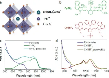
Prior to the fabrication of photodetectors, the structural and optoelectronic properties of dye-perovskite thin-film composites are investigated. In this work, a mixed-cation lead mixed-halide perovskite, FA0.83Cs0.17Pb(I0.9Br0.1)3, is chosen as an active
sensing layer because of its enhanced stability and superior optoelectronic properties.[38,39] Figure 1a schematically depicts
the perovskite structure of FA0.83Cs0.17Pb(I0.9Br0.1)3. In this
stoi-chiometry, the use of the FA-Cs cation mixture leads to an effec-tive ionic radius that fits well within the Goldschmidt tolerance range, stabilizing the structure against deterioration into non-perovskite phases that are not photoactive.[40,41] The band gap of
this perovskite is predominantly influenced by the lead halide octahedral cages, and therefore by the ratio between iodide and bromide content.[42] Here, we fix the I:Br ratio at 9:1 to achieve
[image:3.595.121.472.446.698.2]a smaller band gap (1.55 eV), i.e., a somewhat larger photo-detection bandwidth than for the corresponding pristine iodide
perovskite. Figure 1b displays the chemical structures of the dyes mixed with the perovskite active layer as complementary photoabsorbers, which are 2-[2-[2-chloro-3-[2-(1,3-dihydro-3,3-dimethyl-1-ethyl-2H-benz[e]indol-2-ylidene) ethyli-dene]-1-cy-lohexen-1-yl]-ethenyl]-3,3-dimethyl-1-ethyl-1H-benz[e]indolium hexafluoro-phosphate (CyPF6) and
1-Butyl-2-(2-[3-[2-(1-butyl- 1H-benzo[cd]indol-2-ylidene)-ethyli-dene]-2-diphenylamino-cyclopent-1-enyl]-vinyl)-benzo[cd] indolium tetrafluoroborate (Cy1BF4). Importantly, both dyes are ionic and hydrophilic, and
exhibit good compatibility with OHPs during thin film forma-tion, with no observable aggregation or serious surface rough-ening of the thin film discernible by eye. Figure 1c,d shows the absorption spectra of dyes CyPF6 and Cy1BF4 along with
those for the FA0.83Cs0.17Pb(I0.9Br0.1)3 perovskite and the
corre-sponding composite materials. Based on the rationale outlined above, the incorporated dyes are expected to harvest photons in the NIR and SWIR regimes. As expected, the absorption spectra of the composite thin films are a combination of the absorption features from the perovskite and the dyes, as shown in Figure 1c,d, and hence display significant absorption in the NIR and SWIR regimes. Furthermore, by controlling the blend ratio of the dye and perovskite, it is evidently possible to tailor the absorption spectra and consequently the photoresponse spectra.
2.2. Tuning Optoelectronic Properties through Dye Loading
To verify the tunability of the absorption spectra, we used CyPF6–perovskite composite films prepared with various blend
ratios (volume to volume)—the corresponding absorbance
spectra were normalized to the film thickness and are shown in Figure 2a. As expected, the absorption in the NIR regime improves with increasing dye content, and the perovskite absorption attenuates commensurately. At blend ratios of 1:1 and 2:1, desirable absorption spectra with fairly even spectral response are achieved, which cover a broad range from 450 up to 1000 nm. The composite films with higher dye content (3:1 and 4:1 ratio) display only weak, broadened features in the region of the perovskite absorption (500–750 nm) implying that an excess of dye may inhibit perovskite crystallization. To iden-tify the impact of dye loading on crystallinity, X-ray diffraction patterns of these films were recorded as shown in Figure 2b. Compared with the pristine perovskite film, the 1:1 composite film maintains the perovskite diffraction features around 14°, 20°, 24°, and 28°. However, the peaks exhibit lower intensity and broadened width compared to the pristine perovskite, indi-cating reduced crystallinity or crystallite size. This result is consistent with the broadening of the perovskite absorption fea-tures (Figure 2a) and is further confirmed by scanning electron microscope images that reveal a reduction in grain size upon dye loading (Figure S1, Supporting Information). The 3:1 com-posite films, on the other hand, exhibit typical “yellow phase” nonperovskite diffraction peaks at ≈12°,[43] suggesting that at
high concentrations of the dye the formation of the perovskite structure is inhibited, which may deteriorate the charge trans-port property of the sensing layer (vide infra).
To further assess the photophysical properties of the com-posite films, photoluminescence (PL) spectra were taken for the dye CyPF6, the FA0.83Cs0.17Pb(I0.9Br0.1)3 perovskite, and the
CyPF6–perovskite (1:1) composite film as shown in Figure 2c.
[image:4.595.122.480.434.679.2]The pristine perovskite film shows a strong peak centered at
www.afm-journal.de www.advancedsciencenews.com
1702485 (4 of 7)
790 nm, which can be attributed to PL from the band edge. By comparison, the PL of CyPF6 is not as intense, showing broad
emission from 750 to 1000 nm. The PL spectrum of com-posite CyPF6–perovskite films comprises two distinct peaks: a
CyPF6 feature peak at 880 nm and a stronger perovskite feature
located at the same wavelength as for the pristine perovskite films but having a larger full width at half maximum, most likely as a result of enhanced disorder. The composite films also exhibit more than two orders of magnitude lower PL intensity compared to the pristine perovskite film (Figure S2, Supporting Information), suggesting efficient PL quenching in the pres-ence of CyPF6 molecules. This behavior can be understood
con-sidering the energy levels of the dyes. Both CyPF6 and Cy1BF4
have relatively low highest occupied molecular orbital levels of −4.8 and −4.3 eV, respectively,[7,44] which enable efficient
hole transfer from the perovskite to the dye (Figure S3, Sup-porting Information). Similarly, the positioning of the corre-sponding lowest unoccupied molecular orbital levels of the dyes will help electron extraction from the dyes to the perovskite. Such spatial segregation of electrons and holes in the different phases of the composite should therefore inhibit electron–hole recombination.
To probe the charge-carrier dynamics in these films, time-resolved PL transients were recorded using the time-correlated single photon counting (TCSPC) technique, as shown in Figure 2d and Figure S4 (Supporting Information). At the exci-tation fluence used, these dynamics are governed by mono-molecular charge-carrier recombination with impurities that act as charge traps.[23] The pristine perovskite film shows a
relatively long lifetime of ≈600 ns with a correspondingly small monomolecular rate constant k1 of 1.7 × 10⁶ s−1 (Figure S4,
Supporting Information). These values are consistent with high-quality perovskite exhibiting a relatively low defect den-sity.[41] The PL lifetime for CyPF
6 is found to be shorter than the
resolution of the TCSPC system (≈200 ps) with the PL decay overlapping with the instrument response function. Impor-tantly, for the CyPF6–perovskite composite films PL lifetimes of
≈7 ns (k1= 1.4 × 10⁸) are found, which is much shorter than for
the pristine perovskite film but substantially longer than for the dyes.
Optical-pump THz-probe photoconductivity spectroscopy (OPTP) was used to further probe the charge-carrier dynamics and charge transport properties of the CyPF6–perovskite
com-posites (see the Supporting Information for details about OPTP data collection and analysis). Photoconductivity transients (Figure S5, Supporting Information) display significantly faster apparent higher-order recombination dynamics for the CyPF6–
perovskite (1:1) composite than for the pristine perovskite. Fits to these data reveal effective bimolecular recombination rate constants that are higher by over an order of magnitude for the composite. These trends are again reflective of the smaller crystal grain sizes in the composite, as similar effects have been observed when moving from thin perovskite films to composites infused into mesoporous oxides, for which smaller perovskite grains form.[23,24] However, excellent charge-carrier
mobility values are maintained provided the dye loading is not excessive. For the CyPF6–perovskite (1:1) composite we find a
respectable electron–hole sum mobility of 11 cm2 V−1 s−1, only
somewhat lower than that of the pristine perovskite control
(20 cm2 V−1 s−1). For the CyPF
6–perovskite (2:1) composite;
however, the THz mobility drops to 2 cm2 V−1 s−1, suggesting
that the dye loading is beginning to deteriorate charge perco-lation pathways. These charge-carrier mobility values are sig-nificantly above what would be expected for organic dye solids alone. Hence, we conclude that the incorporation of dyes into a hybrid perovskite matrix extends light absorption well into the SWIR region, while the perovskite host provides long charge-carrier lifetimes and high charge-charge-carrier mobilities that result in improved charge transport and charge extraction, as shown below.
2.3. NIR and SWIR Photodiodes
Photodetector devices were fabricated using the dye-perovs-kite composites as photoactive layers. All photodiode devices were prepared with a planar architecture comprising a photo-active dye-perovskite layer sandwiched between a metal cathode and an indium tin oxide (ITO) transparent anode. Charge transport layers, i.e., [6,6]-Phenyl C61 butyric acid methyl ester
(PC61BM) and poly(3,4-ethylenedioxythiophene):polystyrene
sulfonate (PEDOT:PSS), were also introduced to enhance the charge-carrier collection and suppress the dark current. The full device layer structure is ITO/PEDOT:PSS/dye-perovskite/ PC61BM/Ag. By simply replacing the dye-perovskite active layer
with pristine dye layers, control devices were fabricated for comparison.
It is well known that organic semiconductors have relatively low charge-carrier lifetimes, mobilities, and exciton diffusion lengths, which can limit organic semiconductor performance in homojunction devices when the film is “electrically” thick, i.e., the film is much thicker than the charge-carrier diffu-sion length.[26] However, “thick junctions” are preferable for
manufacturing and device fabrication, which can reduce the probability of pin-holes, reduce the dark current and enhance the repeatability.[45] Not surprisingly, while a CyPF
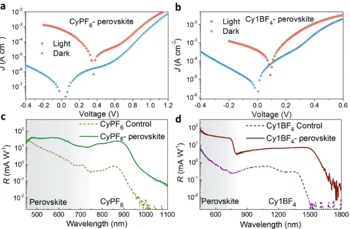
6 control
device with an active layer thickness of 80 nm can generate some photocurrent in the NIR regime, the responsivity values are extremely low (Figure 3c). Here, the low exciton diffusion length of typically ≈3 nm for an organic semiconductor clearly limits the usable range of neat layer thicknesses to ≈10 nm.[44]
By contrast, Figure 3c also presents substantial enhancements by typically over an order of magnitude in responsivity when CyPF6 is added into to the perovskite, even though a thicker
active layer of ≈200 nm is now employed. Typically, the respon-sivity of the photodiodes increased from 0.8 to 24 mA W−1
at 850 nm when the perovskite was added. This concept also shows that from the perspective of perovskite-only detectors, the response is now clearly extended to wavelengths where the perovskite by itself would not induce a photoresponse.[25]
To establish whether this concept could further be imple-mented for the SWIR spectral region beyond 1 µm, we fabri-cated photodiodes based on Cy1BF4–perovskite composites. As
shown in Figure 3d, this low band gap dye contributes a sub-stantial photoresponse from 800 to 1600 nm that again exceeds the responsivity of the Cy1BF4 control device by an order of
particularly exciting as it allows for photon detection at typical fiber-optic communication wavelengths.
Overall, the extension of the photoresponse bandwidth to the NIR and SWIR regions of the spectrum validates our proposal of perovskite-dye composite photodiodes. Here, both com-ponents combine their advantageous properties, with the dye helping to absorb and utilize the NIR and SWIR photons, and the perovskite acting as an excellent host for efficient charge transport. In addition, this broadband perovskite photodetector concept with enhanced NIR and SWIR responsivities allows for further modulation of the responsivity spectra through changes in the dye-perovskite blend ratio, as shown in Figure S6a (Supporting Information). Interestingly, we also find that the responsivity can be enhanced slightly by application of a reverse bias of 0.5 V (Figure S6b, Supporting Information), perhaps through aiding exciton dissociation in the dye.
Finally, we examine the dark current as a critical component for photodetection, which is defined as the current flowing within the device in the absence of illumination. Figure 3a,b presents typical light and dark current–voltage (J–V) curves of the photodiodes based on CyPF6–perovskite and Cy1BF4–
perovs kite composite films, respectively. Normally, dark current and noise current sharply increase with decreasing band gap of the active material at any given temperature.[8] Compared
with pristine perovskite photodiodes,[8] the CyPF
6–perovskite
photodiodes still retain a relatively low room-temperature dark current of the order of 0.01 µA cm−2 without bias, considering
the low dye band gap of 1.25 eV. The SWIR photodiodes based on Cy1BF4–perovskite exhibit much higher dark current of
around 2 µA cm−2 at zero bias which increases dramatically
with increasing bias voltage, possibly due to the small band gap of Cy1BF4 of only 0.82 eV. The measured noise density
spectra (Figure S7, Supporting Information) of these two types of photodiodes show a trend similar to the dark current. The Cy1BF4–perovskite based photodiode exhibits a higher noise
density than that based on CyPF6–perovskite, especially at
−0.5 V bias voltage (Figure S7, Supporting Information). From such accurate measurements of the responsivity and noise cur-rent, the noise equivalent power (NEP) and specific detectivity (D*) can be calculated.[25] The CyPF
6–perovskite based
photo-diodes achieved an NEP of ≈1.5 nW Hz1/2 and D* of 2 × 10⁸
Jones at 900 nm without bias, and the Cy1BF4–perovskite based
devices demonstrate a slightly higher NEP of ≈17 nW Hz1/2 and
lower D* of 2 × 10⁷ Jones at 1500 nm (Figure S8, Supporting
Information).
Another key performance metric is the frequency response, i.e., how fast the detector can respond to the input light signal, which sets the upper limit to the speed of image or data acqui-sition. As shown in Figure 4a, the typical −3 dB point frequency (f−3 dB) roll-off for CyPF6–perovskite based photodiodes is
around 65 kHz, while the Cy1BF4–perovskite devices respond
slightly faster, with f−3 dB of 85 kHz. Typical temporal response
times of the CyPF6–perovskite photodiodes are shown in
Figure 4b, with a rise and fall time of 65 and 74 µs, respectively, in good agreement with the measured frequency response. We note that these devices have relatively large (≈0.1 cm2) and thin
(≈150 nm) active layers, which results in considerable capaci-tance because of the high values of the dielectric function for hybrid metal halide perovskites.[25] It has been reported that the
response time of perovskite photodiodes is mainly determined by the resistance–capacitance constants.[25] With reduced
device area, faster photoresponses have been achieved by Shen et al.[16,46] However, the use of too small a device area may
[image:6.595.124.479.75.307.2]intro-duce substantial errors in the determination of the real active
www.afm-journal.de www.advancedsciencenews.com
1702485 (6 of 7)
area, which will in turn affect the accuracy with which other device parameters can be calculated. To avoid such errors, we therefore decided to investigate devices with an active area of
≈0.1 cm2. Figure 5 further demonstrates the typical transient
photoresponse of the Cy1BF4–perovskite photodiodes
meas-ured at wavelengths above and below the perovskite band gap. We highlight that a fast and highly repeatable response is obtained at SWIR wavelengths, and in particular well into the fiber-optic communications range. Figure S9 of the Supporting Information presents similar temporal response curves for the CyPF6–perovskite photodiodes in the NIR regime. Hence, this
concept clearly allows for detection of photons below the band gap of hybrid metal halide perovskites, with low noise charac-teristics and fast response times.
3. Conclusion
In summary, we have demonstrated a novel method to extend the photoresponse bandwidth of perovskite photodetectors by blending dyes with suitable energetics into hybrid perovskites to create a composite active layer. Ionic, hydrophilic dyes com-patible with perovskite solvents were found to allow for smooth film formation from a mixed precursor solution. Such mixed dye–perovskite composites combined the best of both ingredi-ents, with the small band gap of the dyes enabling collection of NIR and SWIR photons and the perovskite crystals enhancing
the charge transport in the active sensing layer. We further dem-onstrated that the optoelectronic properties of the composite films can be modulated with ease by control of the blend ratio. As a proof of concept, we fabricated prototype photo diodes based on the perovskite composite films which exhibit a broad-band photoresponse covering the majority of the visible, NIR and SWIR spectral ranges. These photodiodes display respect-able responsivities in the range of 10–20 mA W−1 across the
NIR and SWIR regimes, with a response time of around 70 µs, and good dark current and noise characteristics. We conclude that dye-perovskite composite photodetectors are a promising new step for next-generation light sensing across both visible and SWIR regimes at room temperature, with applications in imaging, surveillance, and communications.
Supporting Information
Supporting Information is available from the Wiley Online Library or from the author.
Acknowledgement
The authors acknowledge financial support from the Engineering and Physical Sciences Research Council (EPSRC) U.K. and the European Commission Horizon 2020 Framework (INFORM ITN).
Conflict of Interest
[image:7.595.64.277.75.372.2]The authors declare no conflict of interest. Figure 4. a) Typical frequency response of the NIR and SWIR photodiodes
based on CyPF6–perovskite (2:1) and Cy1BF4–perovskite (2:1), respec-tively, and b) typical rise time and fall time of the NIR CyPF6–perovskite (2:1) photodiodes.
[image:7.595.305.542.77.316.2]Keywords
dye, near-infrared, perovskite, photodiode, short-wavelength infrared
Received: May 9, 2017 Revised: July 11, 2017 Published online: August 4, 2017
[1] G. Konstantatos, E. H. Sargent, Nat. Nanotechnol. 2010, 5, 391. [2] A. Rogalski, J. Antoszewski, L. Faraone, J. Appl. Phys. 2009, 105,
091101.
[3] F. P. G. de Arquer, A. Armin, P. Meredith, E. H. Sargent, Nat. Rev.
Mater. 2017, 2, 16100.
[4] S. A. McDonald, G. Konstantatos, S. Zhang, P. W. Cyr, E. J. Klem, L. Levina, E. H. Sargent, Nat. Mater. 2005, 4, 138.
[5] B. Jalali, S. Fathpour, J. Lightwave Technol. 2006, 24, 4600.
[6] Z. Huang, J. E. Carey, M. Liu, X. Guo, E. Mazur, J. C. Campbell,
Appl. Phys. Lett. 2006, 89, 033506.
[7] M. Young, J. Suddard-Bangsund, T. J. Patrick, N. Pajares, C. J. Traverse, M. C. Barr, S. Y. Lunt, R. R. Lunt, Adv. Opt. Mater. 2016, 4, 1028.
[8] A. Rogalski, Infrared Phys. Technol. 2002, 43, 187.
[9] N. Huo, S. Gupta, G. Konstantatos, Adv. Mater. 2017, 29, 1606576. [10] W. Wang, F. Zhang, M. Du, L. Li, M. Zhang, K. Wang, Y. Wang,
B. Hu, Y. Fang, J. Huang, Nano Lett. 2017, 73, 1995.
[11] J. Miao, F. Zhang, Y. Lin, W. Wang, M. Gao, L. Li, J. Zhang, X. Zhan,
Adv. Opt. Mater. 2016, 4, 1711.
[12] W. Wang, F. Zhang, H. Bai, L. Li, M. Gao, M. Zhang, X. Zhan,
Nanoscale 2016, 8, 5578.
[13] G. Konstantatos, I. Howard, A. Fischer, S. Hoogland, J. Clifford, E. Klem, L. Levina, E. H. Sargent, Nature 2006, 442, 180.
[14] J. P. Clifford, G. Konstantatos, K. W. Johnston, S. Hoogland, L. Levina, E. H. Sargent, Nat. Nanotechnol. 2009, 4, 40.
[15] J. Feng, X. Yan, Y. Liu, H. Gao, Y. Wu, B. Su, L. Jiang, Adv. Mater. 2017, 29, 1605993.
[16] L. Shen, Y. Fang, D. Wang, Y. Bai, Y. Deng, M. Wang, Y. Lu, J. Huang,
Adv. Mater. 2016, 28, 10794.
[17] M. I. Saidaminov, V. Adinolfi, R. Comin, A. L. Abdelhady, W. Peng, I. Dursun, M. Yuan, S. Hoogland, E. H. Sargent, O. M. Bakr, Nat.
Commun. 2015, 6, 8724.
[18] X. Hu, X. Zhang, L. Liang, J. Bao, S. Li, W. Yang, Y. Xie, Adv. Funct.
Mater. 2014, 24, 7373.
[19] W. Zhang, G. E. Eperon, H. J. Snaith, Nat. Energy 2016, 1, 16048. [20] S. D. Stranks, H. J. Snaith, Nat. Nanotechnol. 2015, 10, 391. [21] J. B. Patel, J. Wong-Leung, S. Van Reenen, N. Sakai, J. T. W. Wang,
E. S. Parrott, M. Liu, H. J. Snaith, L. M. Herz, M. B. Johnston, Adv.
Electron. Mater. 2016, 3, 1600470. [22] L. M. Herz, ACS Energy Lett. 2017, 2, 1539.
[23] M. B. Johnston, L. M. Herz, Acc. Chem. Res. 2015, 49, 146. [24] L. M. Herz, Ann. Rev. Phys. Chem. 2016, 67, 65.
[25] Q. Lin, A. Armin, D. M. Lyons, P. L. Burn, P. Meredith, Adv. Mater. 2015, 27, 2060.
[26] Q. Lin, A. Armin, P. L. Burn, P. Meredith, Nat. Photonics 2015, 9, 687.
[27] B. Murali, M. I. Saidaminov, A. L. Abdelhady, W. Peng, J. Liu, J. Pan, O. M. Bakr, O. F. Mohammed, J. Mater. Chem. C 2016, 4, 2545. [28] L. Dou, Y. M. Yang, J. You, Z. Hong, W.-H. Chang, G. Li, Y. Yang,
Nat. Commun. 2014, 5, 5404.
[29] M. I. Saidaminov, M. Haque, M. Savoie, A. L. Abdelhady, N. Cho, I. Dursun, U. Buttner, E. Alarousu, T. Wu, O. M. Bakr, Adv. Mater. 2016, 28, 8144.
[30] Y. Fang, Q. Dong, Y. Shao, Y. Yuan, J. Huang, Nat. Photonics 2015,
9, 679.
[31] S. Yakunin, M. Sytnyk, D. Kriegner, S. Shrestha, M. Richter, G. J. Matt, H. Azimi, C. J. Brabec, J. Stangl, M. V. Kovalenko, Nat.
Photonics 2015, 9, 444.
[32] Y. Liu, J. Sun, Z. Yang, D. Yang, X. Ren, H. Xu, Z. Yang, S. F. Liu,
Adv. Opt. Mater. 2016, 4, 1829.
[33] Q. Lin, A. Armin, P. L. Burn, P. Meredith, Laser Photonics Rev. 2016,
10, 1047.
[34] W. Deng, L. Huang, X. Xu, X. Zhang, X. Jin, S.-T. Lee, J. Jie, Nano
Lett. 2017, 17, 2482.
[35] G. Lin, Y. Lin, H. Huang, R. Cui, X. Guo, B. Liu, J. Dong, X. Guo, B. Sun, Nano Energy 2016, 27, 638.
[36] X. Zhang, S. Yang, H. Zhou, J. Liang, H. Liu, H. Xia, X. Zhu, Y. Jiang, Q. Zhang, W. Hu, Adv. Mater. 2017, 29, 1604431.
[37] C.-j. Teng, D. Xie, M.-x. Sun, S. Chen, P. Yang, Y.-l. Sun, ACS Appl.
Mater. Interfaces 2016, 8, 31289.
[38] D. P. McMeekin, G. Sadoughi, W. Rehman, G. E. Eperon, M. Saliba, M. T. Hörantner, A. Haghighirad, N. Sakai, L. Korte, B. Rech, Science 2016, 351, 151.
[39] Z. Wang, D. P. McMeekin, N. Sakai, S. van Reenen, K. Wojciechowski, J. B. Patel, M. B. Johnston, H. J. Snaith, Adv.
Mater. 2017, 29, 1604186.
[40] Z. Li, M. Yang, J.-S. Park, S.-H. Wei, J. J. Berry, K. Zhu, Chem. Mater. 2015, 28, 284.
[41] W. Rehman, D. P. McMeekin, J. B. Patel, R. L. Milot, M. B. Johnston, H. J. Snaith, L. M. Herz, Energy Environ. Sci. 2017, 10, 361. [42] W. Rehman, R. L. Milot, G. E. Eperon, C. Wehrenfennig, J. L. Boland,
H. J. Snaith, M. B. Johnston, L. M. Herz, Adv. Mater. 2015, 27, 7938. [43] N. J. Jeon, J. H. Noh, W. S. Yang, Y. C. Kim, S. Ryu, J. Seo, S. I. Seok,
Nature 2015, 517, 476.
[44] J. Suddard-Bangsund, C. J. Traverse, M. Young, T. J. Patrick, Y. Zhao, R. R. Lunt, Adv. Energy Mater. 2016, 6, 1501659.
[45] A. Armin, M. Hambsch, I. K. Kim, P. L. Burn, P. Meredith, E. B. Namdas, Laser Photonics Rev. 2014, 8, 924.