Current Processing Current Tunable Universal
Biquad Filter Employing Two CCTAs and
Two Grounded Capacitors
Ravindra Singh Tomar1, Sajai Vir Singh2, Durg Singh Chauhan3
1Department of Electronics Engineering, Anand Engineering College, Agra, India
2Department of Electronics and Communications, Jaypee Institute of Information Technology, Noida, India 3Department of Electrical Engineering, Indian Institute of Technology, Banaras Hindu University, Varanasi, India
Email: [email protected], [email protected], [email protected]
Received July 10, 2013; revised August 10, 2013; accepted August 17,2013
Copyright © 2013 Ravindra Singh Tomar et al. This is an open access article distributed under the Creative Commons Attribution License, which permits unrestricted use, distribution, and reproduction in any medium, provided the original work is properly cited.
ABSTRACT
This paper presents a current processing current-tunable universal biquad filter employing two current conveyor trans- conductance amplifiers (CCTAs) as active element and two grounded capacitors as passive element. It realizes all the five standard filtering responses such as low pass (LP), band pass (BP), high pass (HP), band reject (BR) and all pass (AP) through appropriate selection of applied current inputs. Proposed circuit does not require minus input current sig- nal and double input current signal to realize different filtering responses. It also does not require component matching condition to realize any filtering responses. Moreover, the circuit offers the advantage of orthogonal electronic tunabil- ity of pole-frequency and quality factor. The circuit exhibits low active and passive sensitivities. The circuit perform- ance is verified through P-SPICE simulation software.
Keywords: Biquad; Current-Mode; Universal Filter; CCTA
1. Introduction
The applications, advantages and realizations of high performance continuous-time (CT) current-mode (also called current processing) active filters have been re- ceiving considerable attention, since the last few decades [1,2]. Thus, a number of papers deal with the design of biquad current-mode (CM) filter in the literature [3-27] using different current-mode active elements. However, all of them are realized either in the form of the single- input multiple-output (SIMO) or multiple-input single output (MISO) category. SIMO filters [3-13] simultane- ously realize different filtering functions (in general three or more) at different outputs, without changing the con- nection of the input signal. On the other hand MISO fil- ters [15-27] can realize multifunction filtering responses at single output terminal by altering the way in which multi-input signals are connected. Moreover, the MISO configuration in comparison with SIMO configuration may lead to a reduction in number of active elements for circuit realization and hence, seems to be more suitable than that of SIMO configuration to realize all the stan- dard biquad filter functions. However, one critical issue
with CT filters is the RC time constant variation problem due to process tolerance, the environmental effects of temperature drift, humidity and aging of the components [14]. As a consequence, the performance of the filter circuit differs from the nominal design. The continuous- time filter approach typically compensates for this pro- blem with the tunable filter, by electronically varying the time constant. So there is a growing interest towards de- signing of electronically tunable filters to compensate for deviation in the circuit due to process tolerance, parasitic, temperature drift and component aging. During the last one decade and recent past, several electronically tunable MISO type current-mode active filters have been pro- posed in the literature [15-27], using different current- mode active elements such as second generation current controlled current conveyor (CCCII) [15-21], current dif- ferencing transconductance amplifier (CDTA) [22], cur- rent follower transconductance amplifier (CFTA) [23], voltage differencing transconductance amplifier (VDTA) [24], current controlled transconductance amplifier (CC- TA) [25] and current controlled current conveyor trans- conductance amplifier (CCCCTA) [26,27] etc.
ported in [15-21] uses two [15-17] or more [18-20] CCC- IIs and two grounded capacitors but all of them [15-20] require minus input current signal(s) [15-20] and/or com- ponent matching conditions [18,20] to realize at least one filter function. Thus, they need one or more active com- ponent to obtain minus input current signal/matching condition. The single CCCII-based current-mode filter [21] with three input single output uses two grounded capacitors and one resistor. However, it still needs minus input current signal(s) to realize BP, BR and AP filter functions. Few more three input single output current- mode filters based on two active elements in the form of CDTA [22], CFTA [23], VDTA [24] and CCTA [25] are also proposed in the literature. Each circuit [22-25] con- sists of two grounded capacitors and realizes all the stan- dard filtering functions but they also require minus input current signal(s) [22-24] or/and double input current sig- nal(s) [22-25] to realize at least one filter function. Other novel circuits based on two CCCCTAs [26,27] each having two grounded capacitors can also be used as three input single output tunable current-mode filter but they still require minus input current signal [26] or matching conditions [27] to realize AP response.
In this paper, a current processing current-tunable uni- versal biquad filter is proposed which consists of two current conveyor trans-conductance amplifiers (CCTAs) and two grounded capacitors. It can realize LP, BP, HP, BR and AP in the current form at high impedance output through appropriate selection of the input signals, with- out any matching conditions. Moreover, the proposed circuit realizes all the filtering responses without requir- ing any minus input current signal and double input cur- rent signal. Also, the circuit offers the advantage of elec- tronic tunability of pole-frequency independent of quality factor. The circuit exhibits low active and passive sensi- tivities. The circuit is simulated through P-SPICE simu- lation.
2. CCTA and Proposed Biquad Filter
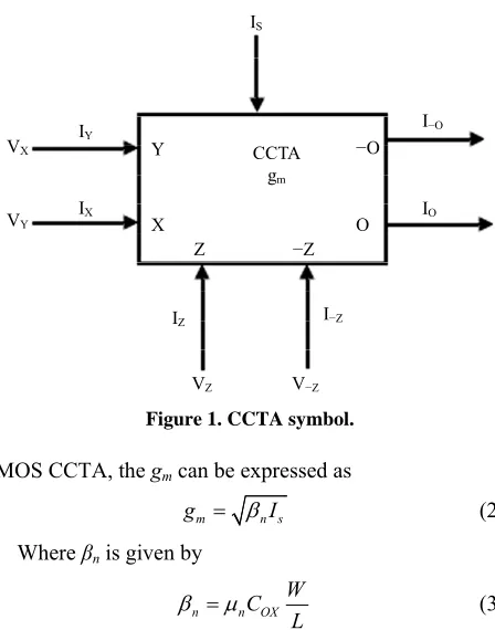
The CCTA [13,25] is a combination of second generation current conveyor (CCII) and operation transconductance amplifier (OTA). The block diagram of the CCTA is shown in Figure 1. It consists of two input terminals (X, Y). Port X is low input impedance terminal while port Y
is the high input impedance terminal. Port ± Z and port ± O are the high output impedance terminals. The input- output current-voltage relationship between different ter- minals of the CCTA can be described by the following equations.
0, , ,
Y X Y Z X O m Z
I V V I I I g V (1)
where gm is the trans-conductance of CCTA and depends
upon the biasing current Is of the CCTA. The MOS im-
plementation of CCTA is proposed in Figure 2. For a
CCTA
gm
Y
X
−O
O
Z −Z
I−O
IO
I−Z
IZ
V−Z
VZ
IY
IX
VX
VY
[image:2.595.310.534.80.365.2]IS
Figure 1. CCTA symbol.
MOS CCTA, the gm can be expressed as
m n s
g I (2) Where βnis given by
n n OX
W C
L
(3)
where μn, COX and W/L are the electron mobility, gate
oxide capacitance per unit area and transistor aspect ratio of M13 and M14 NMOS, respectively.
The proposed current-processing universal filter with three inputs (I1, I2 and I3) and single output (Iout) is shown
in Figure 3. The circuit employs only two CCTAs and
two grounded capacitors. A routine analysis of the circuit in Figure 3 yields the following current output
expres-sion.
21 2 1 2 m2 2 m1 m2 3
out
s C C I sC g I g g I I
D s
(4)
Where
21 2 2 m2 m1 m2
D s s C C sC g g g (5) It is evident from (4) that various biquad filtering re- sponses in current form can be obtained at current output (Iout) through appropriate selection of input cur-
rents.
1) Inverted HP response at Iout, with I1 = Iin, and I2= I3
= 0.
2) Inverted LP response at Iout, with I3 = Iin, I1 = I2 = 0.
3) Non-inverted BP response at Iout, with I2 = Iin, and I1= I3 = 0.
4) Inverted BR response at Iout, with I1 = I3 = Iin, and I2
= 0.
5) Inverted AP response at Iout, with I1 = I2 = I3 = Iin,
VSS
M15
M17
M27 M19 M16
M18
M28 M30
M20
M21 M22
M23 M24
M25 M26
−O +O
M13 M14 −Z
Z Z
X M1 M2
M3 Y
vbb M4 M5 M6 M12 M29 M31
Is
M7
M8
M9 M10 M11
[image:3.595.87.511.92.255.2]VDD
Figure 2. CMOS implementation of CCTA.
−Z +O X
Z
CCTA-1
Y
−O Z
Iout
I2
C2
C1
I3
I1
Z
−Z
X
Y CCTA-2
[image:3.595.107.222.639.711.2]−O +O
Figure 3. Proposed universal current-processing biquad fil- ter.
type input current signal(s) and double input current sig- nal(s) to realize all the responses in the design. Moreover, the proposed circuit also realizes all filtering responses without any component matching condition. The filter parameters such as pole frequency (ω0) and quality factor
(Q0) can be formulated as
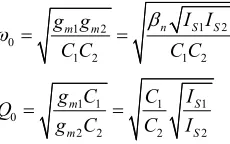
1 2
1 2
0
1 2 1 2
n S S
m m I I
g g
C C C C
(6)
1 1 1 1
0
2 2 2 2
m S
m S
g C C I Q
g C C I
(7)
From (6) and (7), it can be noted that the pole fre- quency can be adjusted by IS1 and IS2 without affecting
the quality factor by keeping the ratio of IS1 and IS2 as
constant. Similarly, Q0 can also be adjusted by IS1 and IS2
without affecting the pole frequency by keeping the product of IS1 and IS2 as constant. In addition, bandwidth
(BW) of the system can be expressed by
2
0 2
0 1 1
n S
m I
g BW
Q C C
(8)
It can also be noted that ω0 and Q0 of the filter can be
simultaneously controlled independent of the BW through
IS1.
3. Non-Ideal Aspects
A non-ideal CCTA, implemented with the transistors is characterized by finite voltage, current and trans-conduc- tance tracking errors occurred due to the mismatching in the transistors. Therefore, taking the non-idealities of the CCTA into account, the relationship of the terminals voltage and current of the ith CCTA described by (1) can
be modified by (9) which is as follows
0, , ,
,
Yi Xi i Yi Zi pi Xi
Zi ni Xi Oi i mi Zi
I V V I I
I I I g V
(9)
Where αpi, αni, βi and γi are the tracking errors of ith
CCTA (ith = 1, 2) and practically deviated from unity.
Taking the non-idealities of CCTA given in (9) into con- sideration and re-analyzing the circuit of Figure 3, the
current response of the proposed circuit of Figure 3 are
changed to
21 2 1 1 2 m2 2 1 1 m1 m2 3
out
s C C I sC g I g g I I
D s
(10)
Where
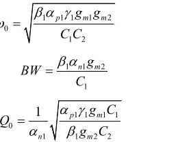
21 2 1 n1 2 m2 1 p1 1 m1 m2
D s s C C sC g g g (11) With involved non-idealities, ω0, Q0 and BW are mo-
1 1 1 1 2 0
1 2
p g gm m C C
(12)
1 1 2
1
ngm
BW C
(13)
1 1 1 1
0
1 1 2 2
1 p m
n m
g C Q
g C
(14)
This shows that ω0 and Q for the ideal current-mode
filter are slightly affected by non-ideal tracking errors. Sensitivity analysis of the proposed filter with respect to active and passive elements yields
0 0
1, 2 1, 1 1, , 1, 2
1 1
,
2 p m m 2
C C g g
S S (15)
0
1, 2, 2,2, 2 0
n p n
S (16)
0 0
2, 2,1 1, 1,1, 1
1, 1
2 2
m p m
Q Q
C g C g
S S (17)
0 0
1 1, 2, 2,2, 2 0
n p n
Q Q
S S (18) From above results, it can be found that all the active and passive sensitivity are within “unity” in magnitude and hence, proposed circuit ensures a good sensitivity performance.
4. Simulation Results
To verify the theoretical analysis of the proposed current- processing filter circuit of Figure 3, PSPICE simulation
has been used. In simulation, the CCTA was realized
using CMOS implementation as shown in Figure 2. The
MOS transistors were simulated using 0.35 um MOS process parameters from TSMC (the model parameters are given in Table 1). The supply voltages were VDD =
−VSS = 1.75 V and Vbb = −0.55 V. The dimensions of
M13 and M14 NMOS were determined as W = 14 µm and L = 2 µm while the dimensions of all remaining NMOS were determined as W = 10 µm and L = 2 µm. In PMOS transistors, the dimensions were W = 10 µm and L = 1 µm. The circuit was designed with IS1 = IS2 = 100
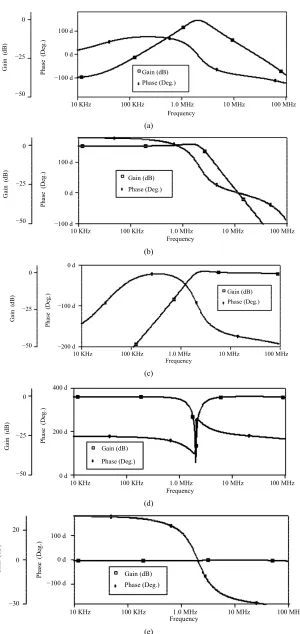
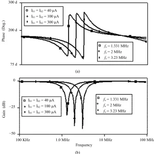
µA, and C1 = C2 = 26 pF. Figure 4 shows the simulated
current gain and phase responses of BP, LP, HP, BR and AP for the proposed current-mode filter. The simulation results show the simulated pole frequency as 2.04 MHz that agree quite well with the theoretical analysis. Fig-ures 5 and 6 shows the responses of BP and BR
func-tions, respectively, where IS1 and IS2 were equally set and
changed for several values, by keeping its ratio to be constant for constant Q0 (= 1). From Figures 5 and 6, it
can be seen that pole frequency can be electronically tuned by the bias currents (IS1 and IS2) without affecting
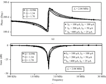
quality factor. Similarly, Q0 tunability independent of
pole frequency is shown in Figures 7 and 8 which dis-
play the BP and BR responses, respectively, for different sets of value of IS1 and IS2 with their product to be main-
tained as constant. The time domain response of current- mode HP output is shown in Figure 9. It was observed
that 120 µA peak to peak input current sinusoidal signal levels having frequency 40 MHz are possible without significant distortions.
5. Conclusion
In this paper, a new current processing current tunable universal biquad filter employing two CCTAs and two grounded capacitors is proposed. The proposed filter of- fers the following advantages: 1) employment of only two active elements; 2) ability of realizing all current-mode standard filtering functions; 3) employment of minimum number of grounded capacitors (only two) to realize any biquad filtering function; 4) low sensitivity figures; 5) electronically orthogonal tunability of ω0 and Q; 6) avail-
ability of explicit current output (i.e. high impedance out- put node) without requiring any additional active elements; 7) no requirement of components matching conditions to get all filtering responses; 8) no requirements of invert- ing-type input current signal(s) and double input current signal(s) to realize the filtering response(s) in the design, all of which are not available simultaneously in any of the previously reported current-controlled current-mode bi- quad filter of [15-27]. With above mentioned features, it is very suitable to realize the proposed circuit in monolithic chip to use in battery powered, portable
Table 1.The SPICE model parameters of MOSFET for level 3, 0.35 µm CMOS process from TSMC.
NMOS
LEVEL = 3 TOX = 7.9E - 9 NSUB = 1E17 GAMMA = 0.5827871 PHI = 0.7 VTO = 0.5445549 DELTA = 0 UO = 436.256147 ETA = 0 THETA = 0.1749684 KP = 2.055786E - 4 VMAX = 8.309444E4 KAPPA = 0.2574081 RSH = 0.0559398 NFS = 1E12 TPG = 1 XJ = 3E - 7 LD = 3.162278E - 11 WD = 7.046724E - 8 CGDO = 2.82E - 10 CGSO = 2.82E - 10 CGBO = 1E - 10 CJ = 1E-3 PB = 0.9758533 MJ = 0.3448504 CJSW = 3.777852E-10 MJSW = 0.3508721
PMOS
[image:4.595.130.260.85.189.2]10 KHz 100 KHz 1.0 MHz 10 MHz 100 MHz Frequency
Gain (dB) Phase (Deg.) 100 d
0 d
−100 d
Ph
as
e (Deg
.)
Ga
in
(d
B
)
0
−25
−50
(a)
Gain (dB) Phase (Deg.)
10 KHz 100 KHz 1.0 MHz 10 MHz 100 MHz Frequency
100 d
0 d
−100 d
Ph
as
e (
D
eg
.)
Ga
in
(
dB
)
0
−25
−50
(b)
Gain (dB) Phase (Deg.)
10 KHz 100 KHz 1.0 MHz 10 MHz 100 MHz Frequency
0 d
−100 d
−200 d
P
ha
se (
D
eg
.)
Ga
in
(
dB
)
0
−25
−50
(c)
400 d
200 d
0 d
Ph
ase (D
eg
.)
Gain
(
dB
)
0
−25
−50
Gain (dB) Phase (Deg.)
10 KHz 100 KHz 1.0 MHz 10 MHz 100 MHz Frequency
(d)
Ga
in
(
dB
)
20
0
−30
Gain (dB) Phase (Deg.)
10 KHz 100 KHz 1.0 MHz 10 MHz 100 MHz Frequency
100 d
0 d
−100 d
Ph
as
e (
D
eg
.)
[image:5.595.149.449.74.708.2](e)
IS1 = IS2 = 40 μA
IS1 = IS2 = 100 μA
IS1 = IS2 = 300 μA
fo = 1.331 MHz
fo = 2 MHz
fo = 3.23 MHz
100 KHz 1.0 KHz 10 MHz 100 MHz Frequency
0
−25
−50
Ga
in
(
dB
[image:6.595.145.445.84.230.2])
Figure 5. BP responses for different value of IS1 = IS2 to show the electronic tunability of pole frequency.
fo = 1.331 MHz
fo = 2 MHz
fo = 3.23 MHz 300 d
200 d
75 d
Ph
as
e (De
g.)
IS1 = IS2 = 40 μA IS1 = IS2 = 100 μA IS1 = IS2 = 300 μA
(a)
IS1 = IS2 = 40 μA IS1 = IS2 = 100 μA IS1 = IS2 = 300 μA
fo = 1.331 MHz
fo = 2 MHz
fo = 3.23 MHz
Ga
in
(
dB
)
0
−25
−50
100 KHz 1.0 MHz 10 MHz 100 MHz Frequency
[image:6.595.146.447.261.562.2](b)
Figure 6. BR responses (a) Gain (b) Phase, for different value of IS1 = IS2 to show the electronic tunability of pole frequency.
IS1 = 100 μA, IS2 = 100 μA
IS1 = 200 μA, IS2 = 50 μA
IS1 =400 μA, IS2 = 25 μA
Ga
in
(
dB
)
0
−20
−40
100 KHz 1.0 MHz 10 MHz 100 MHz Frequency
fo = 2.04 MHz Q = 0.996
Q = 1.34 Q = 1.70
[image:6.595.158.440.594.718.2]IS1 = 100 μA, IS2 = 100 μA
IS1 = 200 μA, IS2 = 50 μA
IS1 =400 μA, IS2 = 25 μA
fo = 2.04 MHz
Q = 0.996 Q = 1.34 Q = 1.70
Ph
as
e (Deg
.)
300 d
200 d
100 d
(a)
Ga
in
(
dB
)
0
−25
−50
300 KHz 1.0 MHz 3.0 MHz 10 MHz 30 MHz Frequency
fo = 2.04 MHz
IS1 = 100 μA, IS2 = 100 μA
IS1 = 200 μA, IS2 = 50 μA
IS1 =400 μA, IS2 = 25 μA
Q = 0.996 Q = 1.34 Q = 1.70
[image:7.595.126.470.84.355.2](b)
Figure 8. BR responses (a) gain (b) phase, for different value of IS1 and IS2 to show the electronic tunability of quality factor.
Sinusoidal Input
HP Output
0 s 20 ns 40 ns 60 ns Time
Am
pl
it
ud
e (
μ
A)
100 uA
0 uA
−100 uA
Figure 9. The time domain input waveform and corresponding response at HP current output.
electronic equipments such as wireless communication system devices.
REFERENCES
[1] B. Wilson, “Recent Developments in Current Conveyors and Current Mode Circuits,” IEE Proceeding-G,Vol. 137, No. 2, 1990, pp. 63-77.
[2] M. A. Ibrahim, S. Minaei and H. A. Kuntman, “A 22.5 MHz Current-Mode KHN-Biquad Using Differential Vol- tage Current Conveyor and Grounded Passive Elements,” Int’l J. Electronics and Communication (AEÜ), Vol. 59, No. 5, 2005, pp. 311-318.
[3] A. M. Soliman, “Current Mode Universal Filter,” Elec-tronics Letters, Vol. 31, No. 17, 1995, pp. 1420-1421.
[4] R. Senani, V. K. Singh, A. K. Singh and D. R. Bhaskar, “Novel Electronically Controllable Current Mode Uni- versal Biquad Filter,” IEICE Electronics Express, Vol. 1, No. 14, 2004, pp. 410-415.
[5] S. Maheshwari, S. V. Singh and D. S. Chauhan, “Elec- tronically Tunable Low Voltage Mixed-Mode Universal Biquad Filter,” IET Circuits, Devices and Systems, Vol. 5, No. 3, 2011, pp. 149-158.
[6] M. T. Abuelma’atti and A. M. Shabra, “A Novel Current Conveyor-Based Universal Current-Mode Filter,” Mi- croelectronics Journal, Vol. 27, No. 6, 1996, pp. 471-475.
[image:7.595.156.443.391.525.2]Controlled Universal Filter with Single Input and Three Outputs,” Int’l J. Electronics, Vol. 88, No. 3, 2001, pp. 333-337.
[8] A. U. Keskin, D. Biolek, E. Hancioglu and V. Biolkova, “Current-Mode KHN Filter Employing Current Differ- encing Transconductance Amplifiers,” Int’l J. Electronics and Communications, Vol. 60, No. 6, 2006, pp. 443-446.
[9] S. V. Singh, S. Maheshwari and D. S. Chauhan, “Univer- sal Current-Controlled Current-Mode Biquad Filter Em- ploying MO-CCCCTAs and Grounded Capacitors,” Jour- nal of Circuits, Systems, and Computers, Vol.1, 2010, pp.
35-40.
[10] T. Tsukutani, Y. Sumi, S. Iwanari and Y. Fukui, “Novel Current-Mode Biquad Using MO-CCCIIs and Grounded Capacitors,” Proceeding of 2005 Symposium on Intelli- gent Signal Processing and Communication (ISPACS), Hong Kong, 13-16 December 2005, pp. 433-436.
[11] B. Singh, A. K. Singh and R. Senani, “New Universal Current-Mode Biquad Using Only Three ZC-CFTA,” Ra- dioengineering, Vol. 21, No. 1, 2012, pp. 273-280. [12] D. Biolek and V. Biolkova, “CDTA-C Current-Mode Uni-
versal 2nd Order Filter,” Proceeding of the 5th WSEAS Int’l Conference on Applied Informatics and Communica- tions, Malta, 15-17 September 2005, pp. 411-414. [13] N. Herencsar, J. Koton and K. Vrva, “Single CCTA-
Based Universal Biquad Filters Employing Minimum Components,” International Journal of Computer and Electrical Engineering, Vol. 1, No. 3, 2009, pp. 307-310. [14] B. Metin, “Electronic Tunability in Analog Filters,” Ph.D.
Thesis, Bogazici University, Istanbul, 2007.
[15] W. Tangsriart and W. Surakampontorm, “Low Compo- nent Current-Mode Universal Filter Using Current Con- trolled Conveyors and Grounded Capacitors,” Journal of Active and Passive Electronic Devices, Vol. 8, 2009, pp. 259-264.
[16] M. Kumngem, J. Chanwutitumt and K. Dejhan, “Cur- rent-Tunable Current-Mode Universal Filter Using Mini- mum Elements,” Proceeding of the 6th IEEE Int’l Con- ference on Electrical Engineering/Electronics and Infor- mation Technology (ECRI-CON), Pattaya, 6-9 May 2009, pp. 582-585.
[17] E. Yuce, A. Kircay and S. Tokat, “Universal Resistorless
Current-Mode Filters Employing CCCIIs,” Int’l Journal of Circuit Theory and Applications, Vol. 36, No. 5-6,
2008, pp. 739-7
[18] W. Tangsriart and W. Surakampontorm, “Electronically Tunable Current-Mode Universal Filter Employing Only Plus-Type Current-Controlled Conveyors and Grounded Capacitors,” Circuits Systems and Signal Processing, Vol. 25, No. 6, 2006, pp. 701-713.
[19] N. Jangsamsi, T. Pukkalanun and W. Tangsrirat, “CCCII- Based High-Output Impedance Current-Mode Universal Filter Employing Only Grounded Capacitors,” SICE- ICASE International Joint IEEE Conference, Busan, 18- 21 October 2006,pp. 5695-5698.
[20] M. T. Abuelma’atti and M. L. Al-qahtani, “Universal Cur- rent-Contolled Current-Mode Filter with Three Inputs and One Output Using Current Controlled Conveyor,” Active Passive Electronic Components, Vol. 21, No. 1, 1998, pp.
[21] C. M. Chang, T. H. Huang, S. H. Tu, C. L. Hou and J. W. Horng, “Universal Active Current Filter Using Single Se- cond-Generation Current Controlled Conveyor,” Circuits, Systems and Signal Processing, Vol. 1, No. 2, 2007, pp. 194-198.
[22] W. Tangsrirat, T. Dumawipata and W. Surakampontorn, “Multiple-Input Single-Output Current-Mode Multifunc- tion Filter Using Current Differencing Transconductance Amplifiers,” Int’l Journal of Electronic and Communica- tion (AEÜ),Vol. 61, No. 4, 2007, pp. 209-214.
[23] S. Lawnwisut and M. Siripruchyanun, “A Current-Mode Multifunction Biquadratic Filter Using CFTAs,” Journal of King Mongkut’s University of Technology, North Bang- kok, Vol. 22, No. 3, 2012, pp. 479-484.
[24] J. Satansup, T. Pukkalanum and W. Tangsrirat, “Elec- tronically Tunable Current-Mode Universal Filter Using VDTAs and Grounded Capacitors,” Proceeding of the In- ternational Multiconference of Engineers and Computer Scientists, Hongkong, 13-15 March 2013, pp. 6-9. [25] T. Thosdeekoraphat, S. Summart, C. Saetiaw, S. Santalu-
nai and C. Thongsopa, “Resistor-Less Current-Mode Uni- versal Biquad Filter Using CCTAs and Grounded Ca- pacitors,” World Academy of Science, Engineering and Technology, Vol. 69, 2012, pp. 559-563.
[26] W. Jaikla, S. Siripongdee and P. Suwanjan, “MISO Cur- rent-Mode Biquad Filter with Independent Control of Pole Frequency and Quality Factor,” Radioengineering Journal, Vol. 21, No. 3, 2012, pp. 886-891.