N A N O E X P R E S S
Open Access
An Investigation on a Crystalline-Silicon
Solar Cell with Black Silicon Layer at the
Rear
Zhi-Quan Zhou
1, Fei Hu
1, Wen-Jie Zhou
1, Hong-Yan Chen
2, Lei Ma
1, Chi Zhang
1and Ming Lu
1*Abstract
Crystalline-Si (c-Si) solar cell with black Si (b-Si) layer at the rear was studied in order to develop c-Si solar cell with sub-band gap photovoltaic response. The b-Si was made by chemical etching. The c-Si solar cell with b-Si at the rear was found to perform far better than that of similar structure but with no b-Si at the rear, with the efficiency being increased relatively by 27.7%. This finding was interesting as b-Si had a large specific surface area, which could cause high surface recombination and degradation of solar cell performance. A graded band gap was found to form at the rear of the c-Si solar cell with b-Si layer at the rear. This graded band gap tended to expel free electrons away from the rear, thus reducing the probability of electron-hole recombination at b-Si and improving the performance of c-Si solar cell.
Keywords:c-Si solar cell, Black silicon, Graded band gap, Surface recombination
Background
Highly surface-etched Si that has been loaded or doped with metal or non-metal ions could exhibit strong and broadband absorptivity [1–6]. This type of Si, or black Si (b-Si), has attracted much attention for its potential application in broadband response photovoltaics [7–9]. To date, investigations of b-Si solar cell have focused on such a configuration that the b-Si layer is at the front of the solar cell [10–19]. In this case, electron-hole pairs induced by the sub-band gap near infrared (NIR) absorption at the b-Si layer are far away from the PN junction zone and cannot be decom-posed by the built-in field to become charge carriers, making the sub-band gap NIR photovoltaic response impossible. It is then conceived that if the b-Si layer is placed at the rear, the NIR absorption-induced electron-hole pairs could be decomposed by the Si/oxide interfacial field at the rear [20] or by a built-in field there if an inter-digitated back contact (IBC) configuration is adopted [21], making the photovoltaic (PV) response of such a
crystalline (c)-Si solar cell extend to the sub-band gap NIR range. Unfortunately, the large specific surface area of b-Si would usually cause high surface recombination, which would severely degrade the solar cell performance [10, 15, 22]. Hence, before we start to study the sub-band gap NIR response of c-Si solar cell, it is necessary to know how large the surface recombination of b-Si could be and how to minimize or avoid its influence [23]. In this work, we studied the PV response of c-Si solar cell with b-Si at the rear and explored the physics underlying our observations.
Methods
Materials
P-type Si<100> wafer (CZ, double-side polish, 10 × 10 × 0.2 mm3 in size, 1–10 Ω cm) was used as the substrate. The Si wafer was ultrasonically cleaned and then dipped in dilute HF(1%), followed by etch-ing in a NaOH/alcohol/H2O (0.5 g/200 ml/200 ml) solution at 90 °C for 15 min to slightly texture the surface for antireflection and then rinsing in de-ionized water. To prepare b-Si at the rear, a Ag layer with apparent thickness of 3 nm was evapo-rated onto one surface of Si substrate as catalyst by
* Correspondence:minglu55@fudan.edu.cn
1Department of Optical Science and Engineering and Shanghai
Ultra-Precision Optical Manufacturing Engineering Center, Fudan University, Shanghai 200433, China
Full list of author information is available at the end of the article
resistance heating in a home-made vacuum chamber with base pressure less than 5 × 10⁻⁴ Pa. After im-mersing the Si wafer in a HF(40%):H2O2(30%):H2O = 1:5:10 solution for 120 s at room temperature, a b-Si layer was formed at that Si surface or at the rear of the solar cell. A phosphorous paste was then deposited onto the other Si surface or the front of the solar cell, followed by annealing at 900 °C for 20 min in nitrogen to form a PN junction. A 20-nm-thick SiO2 layer was evaporated onto the front of the solar cell for surface passivation. For the rear surface passivation, a 10-nm-thick Al2O3 layer was deposited using the technique of atomic layer deposition (ALD) (Beneq TFS 200). An 80-nm-thick ITO layer was deposited onto the front surface as the front electrode. A 2-μm-thick Al layer was evaporated by resistance heating as the rear electrode. A thermal annealing in nitrogen at 425 °C for 5 min was conducted to finalize the preparation of c-Si solar cell. It should be pointed out that in this work, we focused on the effect of b-Si at the rear on the PV response; therefore, the front surface was only slightly textured and not highly etched to form b-Si.
Measurements
The reflectance spectra were measured using a UV-vis-NIR spectrophotometer (Shimadzu, UV-3101PC). The surface morphology was measured with a scan-ning electron microscope (SEM) (Philips, XL 30). The PV parameters of the solar cell were obtained with a solar simulator (Oriel/Newport, model 94023A) under 1-Sun AM1.5G condition. The exter-nal quantum efficiency (EQE) of the solar cell was acquired on a QE system of Oriel/Newport. Transmission electron microscopy (TEM) measurements were carried out on a JEOL EM-3000 system. Surface-emitting photo-luminescence (PL) spectra were recorded by a spectropho-tometer (Ocean Optics USB2000), with a 325-nm He-Cd laser (Melles Griot, model series 74) as the excitation source. The surface potentials of p-type Si and b-Si were measured by a Kelvin probe system (KP Technology SKP5050), the so-called contact potential difference, or CPD identification.
Results and Discussion
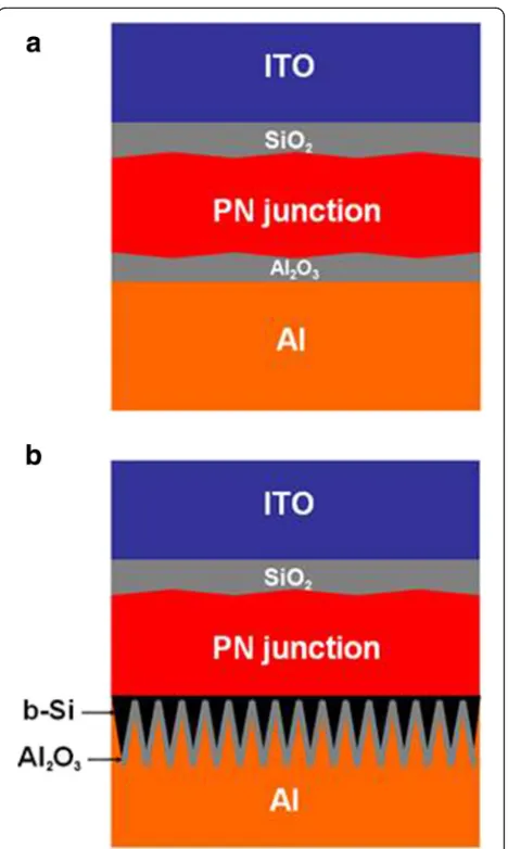
Figure 1a shows a schematic of a slightly surface-textured c-Si solar cell after front and rear passivations. Figure 1b gives a schematic of a simi-larly structured solar cell but with b-Si at the rear. The thickness of the solar cell is approximately 200 μm.
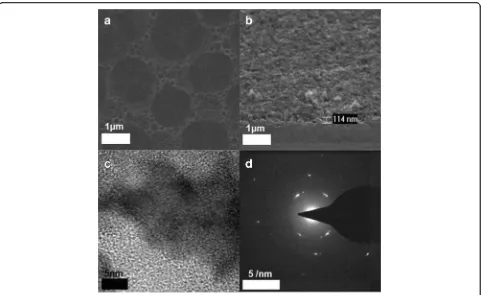
Figure 2a shows a top-view SEM image of the tex-tured front surface. Figure 2b gives a side-view SEM
image of the b-Si surface. The average height of nanostructure of textured Si is 10~20 nm, while that of b-Si is ~ 110 nm. Figure 2c shows a high-resolution (HR) TEM image of b-Si, where the nanocrystalline Si is discernible as reflected by the diffraction fringes. This crystallinity of b-Si is also indicated by the SAED (selected area electron diffrac-tion) pattern as shown in Fig. 2d.
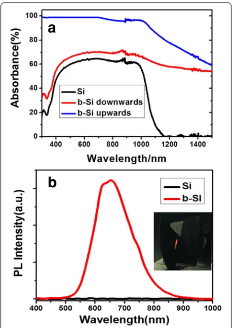
Figure 3a gives the absorption spectra for a wafer Si (termed “Si”), b-Si that faces the incident light (termed “b-Si upwards”), and b-Si with its back toward the incident light (termed “b-Si downwards”). For “Si,” it is seen that when the photon energy is less than the c-Si band gap width (1.1 eV), or equivalently, the wavelength is larger than 1100 nm and almost no absorption occurs as expected. How-ever, for “b-Si upwards,” in addition to the large
[image:2.595.306.540.85.476.2]enhancement of absorption in the 300–1100-nm range due to the strong light trapping by the nano-structures of b-Si [1–9, 24–31], the sub-band gap NIR absorption appears. This sub-band gap absorp-tion could be attributed to the formaabsorp-tion of impurity levels within the band gap, which allows absorption of lower energy photons [25–28, 32]. The sub-band gap absorption can be efficient with the assistance of light trapping [25–28, 32]. For “b-Si downwards,” the absorption in the 300–1100-nm range increases as compared to that of “Si.” It was noticed that although there was no Ag deposited on this front side, it would still be slightly textured during the formation of b-Si at the rear. This surface texturing strengthened the light trapping. It is seen that although part of the sub-band gap NIR is reflected at the front surface, most of the NIR absorbance still remained. This is what one needs for developing a sub-band gap NIR response c-Si solar cell in the future. Figure 3b gives a measured PL spectrum of b-Si, and the inset figure is a photograph of the b-Si under the illumination of the 325-nm laser. No PL emission is found for the Si wafer. The PL emission from b-Si is another indication that Si nanocrystals exist as shown in Fig. 2c [10, 33].
We now investigate how the b-Si at the rear of the c-Si solar cell would affect its performance. In
[image:3.595.58.541.86.381.2]as compared to the “wafer” cell [15, 22]. However, on the contrary, the performance of “b-Si” turns out to be much improved, with its efficiency even close to that of “wafer + Al2O3,” and having a relative 27.7% increase. The EQE curve also shows a consid-erable broadband enhancement. Large surface area-induced high surface recombination seems not to happen here. We then go on to check the cell of“b-Si + Al2O3” and find that after Al2O3passivation at the rear,JSC,VOC, FF, andηfurther increase and so do the EQEs. This indi-cates that Al2O3still passivates efficiently the rear surface as in the case of“wafer + Al2O3.”The role played by b-Si at the rear is unexpectedly interesting and needs to be further explored.
Figure 5 shows an energy band diagram of the PN junction with b-Si at the rear. That the conduction band minimum of b-Si is 0.4 eV above that of p-type Si results from the CPD measurement. Since the b-Si is directly grown on the very p-type b-Si, the dis-tance between the Fermi energy level and the
valence band maximum should basically be kept the same as the doping concentration is the same [37]. Therefore, the band gap width of b-Si is larger than that of wafer Si. This is consistent with the forma-tion of nanocrystalline Si, their PL emission as shown in Figs. 2c and 3b, respectively, and the quantum confinement effect [38]. With such a graded band gap at the rear, free electrons would be expelled away from the b-Si and rear electrode [39];
[image:4.595.56.291.86.417.2]Fig. 4PhotovoltaicJ-V(a) and EQE curves (b) for the solar cells of “wafer,” “wafer + Al2O3,” “b-Si,”and“b-Si+Al2O3”
Table 1Photovoltaic parameters for the solar cells of“wafer,”
“wafer + Al2O3,” “b-Si,”and“b-Si + Al2O3”
Sample Voc(mV) Jsc(mA/cm2) FF (%) η(%)
Wafer 548 30.64 73.33 12.33
Wafer + Al2O3 574 36.49 75.66 15.84
b-Si 571 36.02 76.48 15.75
b-Si + Al2O3 581 38.11 81.02 17.96 Fig. 3Absorption spectra of a wafer Si, b-Si that faces the incident
[image:4.595.309.541.87.450.2] [image:4.595.305.539.661.732.2]meanwhile, the drifting of holes toward the rear electrode is not affected, as indicated in Fig. 5. In that manner, the probability of electron-hole recom-bination at b-Si can be largely reduced and the prob-lem of high surface recombination be efficiently avoided. The formed graded band gap explains why the “b-Si” cell has a far better performance than the “wafer” cell, even though its specific surface area is much larger.
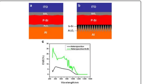
The positive role of b-Si at the rear in photovolta-ics was further manifested in heterojunction struc-tured PV devices as indicated in Fig. 6a, b. As shown in Fig. 6c, for this PV device with b-Si at the rear, the EQE was obviously enhanced as compared to that with no b-Si at the rear. The graded band gap at the interface of P-Si and b-Si should be responsible for the enhancement of EQE [39, 40]. This result is consistent qualitatively with that in Fig. 4b. Although the PV configurations for Fig. 4b and Fig. 6c are different, the role played by the b-Si at the rear is basically the same.
Conclusions
We studied the c-Si solar cell with a b-Si layer at the rear. The c-Si solar cell of such a configuration showed a far better performance than a c-Si solar cell of similar structure but with no b-Si at the rear. This result was attributed to the formation of a graded band gap at the rear, which can largely reduce the probability of surface recombination at the rear, thus improving the performance of the c-Si solar cell. The finding of this work can be applied to developing a c-Si solar cell with broadband PV response, including the sub-band gap NIR response, in the future.
Fig. 5Energy band diagram of the PN junction with b-Si at the rear
[image:5.595.57.290.87.234.2] [image:5.595.58.542.428.713.2]Acknowledgements
The authors would thank Jun-Yi Gong for CPD measurement.
Funding
This work was supported by the National Natural Science Foundation of China (51472051, 61275178) and the CIOMP-Fudan University joint foundation (FC2017-001).
Authors’Contributions
ZQZ prepared all the samples and measured theI-Vand EQE data. FH and WJZ measured the SEM data and TEM data. HYC helped to grow the Al2O3 passivation layer. LM and CZ measured the reflectance data and PL data. ML designed the experiments and wrote the manuscript. All authors read and approved the final manuscript.
Competing Interests
The authors declare that they have no competing interests.
Publisher’s Note
Springer Nature remains neutral with regard to jurisdictional claims in published maps and institutional affiliations.
Author details 1
Department of Optical Science and Engineering and Shanghai
Ultra-Precision Optical Manufacturing Engineering Center, Fudan University, Shanghai 200433, China.2Department of Micro-electronics, Fudan University,
Shanghai 200433, China.
Received: 8 November 2017 Accepted: 28 November 2017
References
1. Huang Z, Geyer N, Werner P, De Boor J, Gösele U (2011) Metal-assisted chemical etching of silicon: a review. Adv Mater 23(2):285–308
2. Peng K, Lu A, Zhang R, Shuit Tong L (2008) Motility of metal nanoparticles in silicon and induced anisotropic silicon etching. Adv Funct Mater 18(19): 3026–3035
3. Toor F, Miller JB, Davidson LM, Nichols L, Duan W, Jura MP, Yim J, Forziati J, Black MR (2016) Nanostructured silicon via metal assisted catalyzed etch (MACE): chemistry fundamentals and pattern engineering. Nanotechnology 27(41):412003
4. Cao Y, Liu A, Li H, Liu Y, Qiao F, Hu Z, Sang Y (2011) Fabrication of silicon wafer with ultra low reflectance by chemical etching method. Appl Surf Sci 257(17):7411–7414
5. Lv H, Shen H, Jiang Y, Gao C, Zhao H, Yuan J (2012) Porous-pyramids structured silicon surface with low reflectance over a broad band by electrochemical etching. Appl Surf Sci 258(14):5451–5454
6. Hao Z, Guo A, Guo G, Wei L, Jiang Y (2016) The enhanced light absorptance and device application of nanostructured black silicon fabricated by metal-assisted chemical etching. Nanoscale Res Lett 11(1):322–327
7. Otto M, Algasinger M, Branz H, Gesemann B, Gimpel T, Füchsel K, Käsebier T, Kontermann S, Koynov S, Li X (2015) Black silicon photovoltaics. Adv Opt Mater 3(2):147–164
8. Xia Y, Liu B, Liu J, Shen Z, Li C (2011) A novel method to produce black silicon for solar cells. Sol Energy 85(7):1574–1578
9. Yuan HC, Yost VE, Page MR, Stradins P, Meier DL, Branz HM (2009) Efficient black silicon solar cell with a density-graded nanoporous surface: optical properties, performance limitations, and design rules. Appl Phys Lett 95(12):123501
10. Wang LX, Zhou ZQ, Hao HC, Lu M (2016) A porous Si-emitter crystalline-Si solar cell with 18.97% efficiency. Nanotechnology 27(42):425207 11. Zhao Z, Li P, Wei Y, Lu C, Tan X, Liu A (2014) 17.3% efficient black silicon
solar cell without dielectric antireflection coating. Sol Energy 110:714–719 12. Shieh J, You C, Chiu C, Liu J, Shih P (2016) Black-silicon on micropillars with
minimal surface area enlargement to enhance the performance of silicon solar cells. Nanoscale Res Lett 11(1):489–496
13. Koynov S, Brandt MS, Stutzmann M (2010) Black multi-crystalline silicon solar cells. Phys Status Solidi-R 1(2):R53–R55
14. Davidsen RS, Li H, To A, Wang X, Han A, An J, Colwell J, Chan C, Wenham A, Schmidt MS (2016) Black silicon laser-doped selective emitter solar cell with 18.1% efficiency. Sol Energ Mat Sol C 144:740–747
15. Oh J, Yuan HC, Branz HM (2012) An 18.2%-efficient black-silicon solar cell achieved through control of carrier recombination in nanostructures. Nat Nanotechnol 7(11):743–748
16. Repo P, Benick J, Vähänissi V, Schön J, Gastrow GV, Steinhauser B, Schubert MC, Hermle M, Savin H (2013) N-type black silicon solar cells. Energy Procedia 38:866–871
17. Savin H, Repo P, Gastrow GV, Ortega P, Calle E, Garín M, Alcubilla R (2015) Black silicon solar cells with interdigitated back-contacts achieve 22.1% efficiency. Nat Nanotechnol 10(7):624–635
18. Ortega P, Calle E, Gastrow G, Repo P, Carrió D, Savin H, Alcubilla R (2015) High-efficiency black silicon interdigitated back contacted solar cells on p-type and n-p-type c-Si substrates. Prog Photovolt Res Appl 23(11):1448–1457 19. Ziegler J, Haschke J, Käsebier T, Korte L, Sprafke AN, Wehrspohn RB (2014)
Influence of black silicon surfaces on the performance of back-contacted back silicon heterojunction solar cells. Opt Express 22(S6):A1469–A1476 20. Zhou Z Q, Hu F, Lu M (2017) A broadband response Si solar cell achieved
by strong rear field passivation combined with sub-band gap infrared absorption. Chinese patent pending, appl num: 2017106029149 21. Zhou Z Q, Hu F, Dai X Y, Lu M (2017) A broadband response interdigitated
back contact Si solar cell. Chinese patent pending, appl num: 2017108154285
22. Otto M, Kroll M, Kasebier T, Salzer R (2012) Extremely low surface recombination velocities in black silicon passivated by atomic layer deposition. Appl Phys Lett 100(19):191603
23. Gastrow GV, Ortega P, Alcubilla R, Husein S, Nietzold T, Bertoni M, Savin H (2017) Recombination processes in passivated boron-implanted black silicon emitters. J Appl Phys 121(18):185716
24. Bett AJ, Bläsi B, Savin H, Goldschmidt JC, Eisenlohr J, Höhn O, Repo P (2016) Wave optical simulation of the light trapping properties of black silicon surface textures. Opt Express 24(6):A434–A445
25. Kim TG, Warrender JM, Aziz MJ (2006) Strong sub-band-gap infrared absorption in silicon supersaturated with sulfur. Appl Phys Lett 88(24):241902 26. Wu C, Crouch CH, Zhao L, Carey JE (2001) Near-unity below-band-gap
absorption by microstructured silicon. Appl Phys Lett 78(13):1850–1852 27. Wang ZY, Zhang RJ, Wang SY, Lu M, Chen X, Zheng YX, Chen LY, Ye Z, Wang CZ, Ho KM (2015) Broadband optical absorption by tunable Mie resonances in silicon nanocone arrays. Sci Rep-UK 5:7810–7815 28. Jiang J, Li S, Jiang Y, Wu Z, Xiao Z, Su Y (2013) Mechanism of optical
absorption enhancement of surface textured black silicon. J Mater Sci-Mater EL 24(2):463–466
29. Yu P, Wu J, Liu S, Xiong J, Jagadish C, Wang ZM (2016) Design and fabrication of silicon nanowires towards efficient solar cells. Nano Today 11(6):704–737 30. Wu J, Yu P, Susha AS, Sablon KA, Chen H, Zhou Z, Li H, Ji H, Niu X, Govorov
AO (2015) Broadband efficiency enhancement in quantum dot solar cells coupled with multispiked plasmonic nanostars. Nano Energy 13:827–835 31. Yu P, Yao Y, Wu J, Niu X, Rogach AL, Wang Z (2017) Effects of plasmonic metal core-dielectric shell nanoparticles on the broadband light absorption enhancement in thin film solar cells. Sci Rep-UK 7(1):7696–7705
32. Peng Y, Chen X, Zhou Y, Xu G (2014) Annealing-insensitive“black silicon” with high infrared absorption. J Appl Phys 116(7):073102
33. Melnichenko MM, Svezhentsova KV, Shmyryeva AN (2005) Porous silicon upon multicrystalline silicon: structure and photoluminescence. J Mater Sci 40(6):1409–1412
34. Schmidt J, Merkle A, Brendel R, Hoex B, Sanden MCMV, Kessels WMM (2008) Surface passivation of high-efficiency silicon solar cells by atomic-layer-deposited Al2O3. Prog. Photovolt Res Appl 16(6):461–466
35. Hoex B, Heil SBS, Langereis E, Sanden MCMV, Kessels WMM (2006) Ultralow surface recombination of c-Si substrates passivated by plasma-assisted atomic layer deposited Al2O3. Appl Phys Lett 89(4):042112
36. Jia X, Zhou C, Wang W (2017) Optimization of the surface structure on black silicon for surface passivation. Nanoscale Res Lett 12(1):193–199
37. Grundmann M (2010) The physics of semiconductors. Springer, New York 38. Prasad PN (2004) Nanophotonics. Wiley, Hoboken
39. Sassi G (1983) Theoretical analysis of solar cells based on graded band-gap structures. J Appl Phys 54(9):5421–5427