N A N O E X P R E S S
Open Access
Wetting layer evolution and its temperature
dependence during self-assembly of InAs/GaAs
quantum dots
Hongyi Zhang, Yonghai Chen
*, Guanyu Zhou, Chenguang Tang and Zhanguo Wang
Abstract
For InAs/GaAs(001) quantum dot (QD) system, the wetting layer (WL) evolution and its temperature dependence were studied using reflectance difference spectroscopy and were analyzed with a rate equation model. WL
thicknesses showed a monotonic increase at relatively low growth temperatures but showed an initial increase and then decrease at higher temperatures, which were unexpected from a thermodynamic understanding. By adopting a rate equation model, the temperature dependence of QD formation rate was assigned as the origin of different WL evolutions. A brief discussion on the indium desorption was given. Those results gave hints of the kinetic aspects of QD self-assembly.
Keywords:Quantum dots, Stranski-Krastanov growth mode, Wetting layer, Desorption, Growth kinetics
PACS: 81.07.Ta, 81.05.Ea, 68.08.Bc, 78,67,Hc, 68.35.Rh
Background
Epitaxial semiconductor quantum dots (QDs) have attracted much attention because of their application po-tential in novel optoelectronic devices [1-3]. They are usually fabricated utilizing the lattice mismatch between the epitaxial layer and substrate or the Stranski-Krastanov (SK) growth mode. It can be described as follows: for small coverage, two-dimensional (2D) layer-by-layer growth and pseudomorphic formation of wet-ting layer (WL) take place. When the WL reaches a cer-tain critical thickness (CT), a 2D to three-dimensional (3D) transition starts, and QDs form on the substrate. QDs with high homogeneity in their size and shape are highly advantageous in applications. Basically, the WL configuration would also influence the optical properties of QDs and the performance of QD-based devices [4-7]. A controllable growth of QDs with desired properties requires a comprehensive understanding on the growth process. Therefore, it is necessary to have a clear under-standing of the WL evolution during the QD self-assembly.
The commonly accepted thermodynamic understand-ing of the SK mode describes the QD formation on top of a WL of a certain thickness. However, it is not accur-ate in real situations. It has been reported that in the Ge/Si QD system, the WL thickness decreases after QD formation [8-10]. It is interpreted in the regime of kinet-ically controlled QD formation and growth. Since mater-ial transfer from WL to QDs sustains the QD formation and growth, a large material consumption rate by QD formation may induce the observed WL erosion [8,9]. As for InAs/GaAs system, a step erosion of WL has also been observed after QD formation [11,12]. Until now, there is no complete description of the WL evolution and its growth condition dependence. In our previous work, reflectance difference spectroscopy (RDS) was used to study the WLs in self-assembled nanostructures. Due to its sensitivity, heavy hole (HH)- and light hole (LH)-related transition energies before and after QD for-mation can be directly obtained from the resonant struc-tures in the spectra [13-16]. In this paper, we studied the WL evolution and its temperature dependence based on RDS measurements. We found that, generally, there were two kinds of WL evolution, with deposition de-pending on growth temperatures. They were well explained in the regime of temperature dependence of * Correspondence:[email protected]
Key Laboratory of Semiconductor Materials Science, Institute of
Semiconductors, Chinese Academy of Sciences, PO Box 912, Beijing, 100083, People's Republic of China
QD growth rate with a rate equation model. The concave-up style of evolution was considered as a clear evidence for a non-zero QD growth rate when the WL thickness was smaller than the CT. We also gave a sim-ple discussion on indium desorption during self-assem-bly. All of these results showed the kinetic aspects of WL evolution in the SK growth.
Methods
Six InAs/GaAs(001) QD samples with different growth temperatures (from 490°C to 540°C, with an increment of 10°C) were grown in our Riber-32p molecular beam epitaxy (MBE) system. A 100-nm GaAs buffer layer was firstly deposited on 2-in semi-insulating GaAs substrates at 600°C. A nominal InAs amount of 2.0 monolayer (ML) (1.9 ML for the sample grown at 510°C) was then deposited with a calibrated rate of 0.1 ML/s at a con-trolled substrate temperature. A gradually changed InAs amount was achieved by stopping the substrate rotation. This method was widely used in studying the QD growth dynamics and to fabricate QD samples with low areal density [8,10,13,17]. The effective indium flux and real deposition amount could be calibrated based on the cosine law for certain configurations of the MBE source beam [18]. Growth interruption (GI) of 10 s was intro-duced after InAs layer deposition. A 100-nm GaAs cap-ping layer was then grown at 600°C. Details of the sample growth processes can be found in another study [16]. For further spectroscopy measurements, the sam-ples were cut into 16 pieces along the direction corre-sponding to which the InAs amount increased gradually.
To evaluate the WL information, the relative reflectance difference in the sample surface plane, i.e., r=r¼ 2 r½110r½110
= r½110þr½110
, was measured with the RDS technique in ambient conditions. The setup of our RDS was reported elsewhere [19].
[image:2.595.59.540.476.675.2]Results and discussion
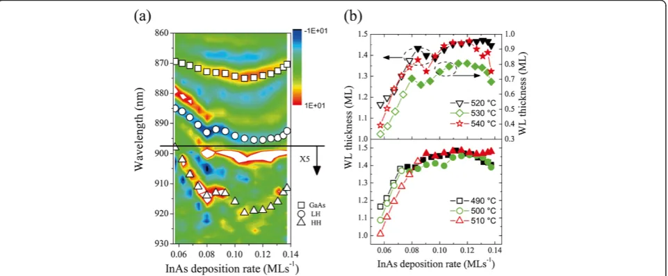
Figure 1a shows the intensity map of the second-derivative spectra obtained from the samples grown at 530°C, in which the distinctive features of the GaAs band edge, LH and HH, of the WLs can be distin-guished. For the horizontal axis, the InAs deposition rate is calibrated with the cosine law mentioned above. One can see the LH and HH transition energies redshift al-most linearly up to an InAs deposition rate of 0.085 ML/s (corresponding to an InAs amount of 1.7 ML), which is commonly known as the CT of InAs QD for-mation, then gradually saturate for further deposition. In order to have an intuitive understanding on the evolu-tion, we calibrate the WL thicknesses based on the tran-sition energies obtained from the spectra [20]. Figure 1b gives the WL thickness evolution of the six samples. The WL thicknesses are signed with open symbols for 2D growth stage and solid symbols for 3D growth stage based on our previous results [16]. In general, two dis-tinct evolution processes can be discerned. An initially increased and then saturated evolution mode was observed in the samples grown at lower temperatures, while distinct concave-up features of the WL evolution for samples with relatively higher growth temperatures
Figure 1Second-derivative spectra and WL thickness evolution.(a) The second-derivative spectra (d2ρ/dλ2) of the series of samples grown
appeared right after QD formation. They are unexpected based on thermodynamic understanding of the SK growth, for which a stable WL thickness is expected dur-ing and after QD formation. There is another decrease of the WL thickness for the last three pieces of each sample. The generation of large QDs, dislocation during the QD ripening process, and the enhanced indium ab-sorption abilities by them can be accounted for the de-crease [14,21].
In describing the WL growth dynamics, we consider three main InAs distribution processes. The newly deposited InAs can be incorporated into the WL and QDs or re-evaporated through the indium desorption process. Other processes, such as the formation of quasi-QDs or indium droplets, are neglected for their relatively lower rates [22,23]. In our previous works, the CTs of those samples were successfully determined, which enabled us to consider the 2D and 3D growth stages separately in this rate equation model [16]. For 2D growth stage, the deposited material contributes to a pseudomorphic growth of the WL and the formation of QDs is neglected. Based on material balance, the rate equation can be written as follows:
dθ
dt ¼G
θ
τdes;ðt<tcÞ; ð1Þ
where θ is the WL thickness, tc is the time of the 2D growth stage, andGis the InAs deposition rate. The in-dium desorption rate is presumed to be proportional to the InAs amount in WL, andτdesrepresents the desorp-tion time constant. The indium desorpdesorp-tion process is generally considered as thermally activated [23,24]; τdes can be written as τdes¼ 1
ν0exp
Edes kT
, where v0 is a pre-exponential factor and Edes is the activation energy of the indium desorption process. By solving Equation 1, the WL thickness versus growth time can be written as follows:
θ¼Gτdes 1exp t
τdes
:ðt<tcÞ ð2Þ
Above the CT, a large amount of QDs appears, and the newly deposited InAs are mainly consumed by them. The rate equation can be written as follows:
dθ
dt ¼G
θ
τdesFQD:ðt>tcÞ ð3Þ
Here FQD is used to represent the InAs consumption rate by the QD formation and growth [25].FQDis deter-mined by the instability of WL and the material diffu-sion from WL to QDs [26]. The diffudiffu-sion rate can be written as DIn= (2kBT /h) exp (−Edif /kBT), [26] where kB is Boltzmann's constant, h is Planck's constant, T is the substrate temperature andEdifis the energy barrier.
In previous works, for a WL thickness ofθ, the instabil-ity of WL is commonly considered as (θ−θc). The driv-ing force of QD growth, which is known as ‘superstress’, is defined as ξ = (θ − θc) / θc [27]. However, it is not suitable in describing our experimental results. The concave-up style of evolution shown in the upper panel of Figure 1b means a non-zero QD growth rate when the WL thickness is slightly below the CT, or else, the WL thickness would not reduce below the CT in the presence of sufficient InAs supply. A non-stopping QD formation when the WL thickness is smaller than the CT is also documented in previous experiments [28-30]. Hence, the unstable part of WL is written as (θ −αθc), (0 <α< 1); correspondingly, the superstress is written as
ξ = (θ −αθc) /αθc (0 <α < 1). The QD formation and growth rate γ is considered to be exponentially dependent on the superstress orγ=b exp (βξ), whereb and β were constant parameters [31,32]. Consequently, FQDcan be written as follows:
FQD¼bðθαθcÞ
2kBT
h exp Edif=kBT
expð Þβξ :
ð4Þ
From Equation 3, it is clear that an equilibrium WL thickness is reached when the deposition rate equals to the WL consumption rate by QD formation and indium
desorption. The last two processes show strong
thickness would suffer a decrease if the deposition rate is not large enough to sustain the QD growth at the be-ginning of the 3D evolution stage. FQD then drops cor-respondingly according to its dependence on the superstress. It takes some time for the WL thickness to be stable to a certain value, for which the material de-position and the QD growth reach a balance. The bigger the deposition rate is, the thicker the stabilized WL. However, if the QD formation rate for the critical WL thickness is lower than the corresponding deposition rate, e.g., a lower growth temperature, WL thickness would keep on increasing after QD formation, which is the case in Figure 2a.
To understand the experimental results, we have to apply the above-mentioned model to the non-rotating samples. The WL thicknesses after deposition can be known by calculating the resulting WL thicknesses with gradually changed InAs deposition rates and a given
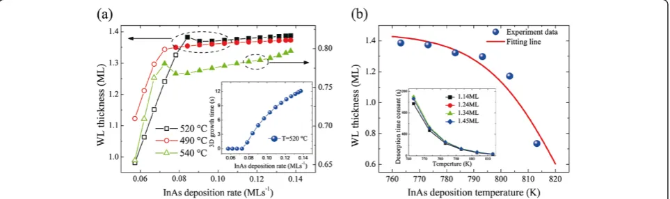
[image:4.595.59.540.90.238.2]deposition time. Considering the WL evolution during GI, one can simply set G= 0 in Equations 2 and 3 and calculate with the WL thicknesses after deposition as initial values. The simulation results of WL evolution at different temperatures are shown in Figure 3a. One could see that the main features are well reproduced compared with the experimental results. The WL thick-ness shows a monotonic increase if the temperature is set at 490°C but shows a concave-up evolution for tem-peratures of 520°C and 540°C. According to the discus-sion above, we know that the slowed down increase observed at lower temperature is because of the depos-ition rate dependence of the equilibrium WL thickness. For higher growth temperatures, the elevated QD forma-tion rate at the beginning of the 3D growth stage led to WL erosion, which corresponds to the decrease of WL thickness on those non-rotating samples. WL thickness increases again with the deposition rate when the growth
Figure 2Calculation results of WL growth dynamics for different InAs deposition rates at (a) 490°C and (b) 520°C.The horizontal and vertical dotted lines correspond to the critical thickness andt= 20 s, respectively. The insets of (a) and (b) zoom in the 3D growth stages. Here, we useb= 8.3 × 10⁻⁹,α= 0.85,β= 10, andE
dif= 1.04 eV to solve the rate equations numerically.
Figure 3Simulation of the WL evolution and fitting result of temperature dependence.(a) Simulation of WL evolution of the non-rotating samples at three different temperatures. The open and closed symbols stand for 2D and 3D growth stages, respectively. Here, we use
b= 4 × 10⁻⁹,α= 0.8,β= 10, andE
dif= 1.04 eV to solve the rate equations numerically. The inset of (a) is the dependence of 3D growth time on
[image:4.595.58.540.522.665.2]reaches equilibrium. It should also be noted that the simple equations do not reproduce the experimental results quantitatively because of their semi-empirical na-ture and the use of some adjustable parameters.
We would like to comment on a special feature of those non-rotating samples. The material deposition rate changes gradually at different positions of a sample, which leads to the same behavior of deposition amount for a given growth time. Considering a weak dependence of the CT on deposition rate, one would expect that it takes different times at those positions of the sample to enter the 3D growth stage. The 2D growth timet2Dcan be calculated respectively from Equation 2 by takingθ =θc. One then obtains the 3D growth time t3D = tInAs− t2D. The inset of Figure 3a shows the 3D growth time with deposition rates. It should be noticed that at some posi-tions, they have very small values. Apparently, a near-zero 3D growth time cannot ensure an equilibrium quantum dot growth nor provide a steady-state WL thickness. It leads to stronger kinetic control characters on those samples.
We come back to the 2D growth stage and to study another kinetic problem during growth - the indium de-sorption. In Figure 1b, for samples with the same depos-ition amount but different growth temperatures, WL thicknesses varied a lot. From Equation 1, we know that it is because of the temperature dependence of indium desorption rate. From Equation 2 and from further con-sidering the WL evolution during GI, the resulting WL thickness in the 2D growth stage can be written as fol-lows:
θ¼Gτdes 1 exp tInAs
τdes
exp tGI
τdes
; ð5Þ
wheretInAsis the InAs deposition time andtGIis the GI time. The kinetic parameter of indium desorption, Edes, and ν0, can be extracted from Equation 5 and Figure 1b. We adopt the WL thicknesses of the first four pieces of each sample with effective InAs deposition amounts of 1.14, 1.24, 1.34, and 1.45 ML to fit Edesand ν0, respect-ively. The obtained Edes = 3.68 eV and ν0 are around 5.5 × 10²². The activation energy is close to previously reported InAs decomposition energy and indium de-sorption activation energy from InGaAs [23,33]. We no-tice that the fittingν0is such a big number;ν0stands for the attempt frequency of desorption, which is commonly known with the order of 1012 to 1014 s−1for desorption from metal and semiconductor surfaces. Such a big tran-sition frequency obtained here is also reported by other groups in investigating the InAs/GaAs QD desorption [33] or As desorption from GaAs surface [34]. It is con-sidered as physically achievable and could explain sev-eral characteristic features in InAs MBE growth [34].
The inset of Figure 3b shows the temperature depend-ence of the desorption life time (τdes) for samples with different InAs deposition amounts based on the fitting results. The time constants show a weak dependence on the indium flux but strongly decrease with increasing temperature;τdesdecreases from 1,063 s at 490°C to 35 s at 540°C for samples with a deposition amount of 1.45 ML. The same strong dependence is also mentioned elsewhere [35]. Those time constants could be used to estimate the degree of desorption during the growth of InAs/GaAs(001) QDs at a certain temperature.
Conclusions
In conclusion, two kinds of WL evolution process of InAs/GaAs(001) QD system have been discussed based on RDS measurements and a rate equation model. They were well understood in the regime of material balance of WL growth/consumption and temperature dependence of QD formation. The concave-up style of evolution is also an evidence of a non-zero QD growth rate when the WL thickness was slightly lower than the critical value. We also gave a brief discussion on the indium desorption process during growth. Those results helped us in under-standing the kinetically controlled QD growth process.
Competing interests
The authors declare that they have no competing interests.
Authors’contributions
HZ carried out the analysis and simulation. GZ and CT did the
measurements. HZ and YC drafted the manuscript. YC and ZW supervised the works. All authors read and approved the final manuscript.
Acknowledgments
The work was supported by the National Natural Science Foundation of China (no. 60990313), the 973 program (2012CB921304, 2012CB619306), and the 863 program (2011AA 03A 101).
Received: 7 September 2012 Accepted: 10 October 2012 Published: 30 October 2012
References
1. Bimberg D, Grundmann M, Ledentsov NN:Quantum Dot Heterostructures. Chichester: Wiley; 1999.
2. Weng GE, Ling AK, Lv XQ, Zhang JY, Zhang BP:III-Nitride-based quantum dots and their optoelectronic applications.Nano-Micro Lett2011,
3:200–207.
3. Ellis B, Mayer MA, Shambat G, Sarmiento T, Harris J, Haller EE, Vuckovic J:
Ultralow-threshold electrically pumped quantum-dot photonic-crystal nanocavity laser.Nat Photon2011,5:297–300.
4. Sanguinetti S, Henini M, Grassi Alessi M, Capizzi M, Frigeri P, Franchi S:
Carrier thermal escape and retrapping in self-assembled quantum dots. Physical Review B1999,60:8276.
5. Wang LJ, Krapek V, Ding F, Horton F, Schliwa A, Bimberg D, Rastelli A, Schmidt OG:Self-assembled quantum dots with tunable thickness of the wetting layer: role of vertical confinement on interlevel spacing. Physical Review B2009,80:085309.
6. Deppe DG, Huffaker DL:Quantum dimensionality, entropy, and the modulation response of quantum dot lasers.Appl Phys Lett2000,77:3325. 7. Matthews DR, Summers HD, Smowton PM, Hopkinson M:Experimental
8. Bergamaschini R, Brehm M, Grydlik M, Fromherz T, Bauer G, Montalenti F:
Temperature-dependent evolution of the wetting layer thickness during Ge deposition on Si(001).Nanotechnology2011,22:285704.
9. Osipov AV, Schmitt F, Kukushkin SA, Hess P:Stress-driven nucleation of coherent islands: theory and experiment.Appl Surf Sci2002,188:156–162. 10. Brehm M, Montalenti F, Grydlik M, Vastola G, Lichtenberger H, Hrauda N,
Beck MJ, Fromherz T, Schäffler F, Miglio L, Bauer G:Key role of the wetting layer in revealing the hidden path of Ge/Si(001) Stranski-Krastanow growth onset.Physical Review B2009,80:205321.
11. Placidi E, Arciprete F, Sessi V, Fanfoni M, Patella F, Balzarotti A:Step erosion during nucleation of InAs/GaAs(001) quantum dots.Appl Phys Lett2005,
86:241913–3.
12. Arciprete F, Placidi E, Sessi V, Fanfoni M, Patella F, Balzarotti A:How kinetics drives the two- to three-dimensional transition in semiconductor strained heterostructures: the case of InAs/GaAs(001).Appl Phys Lett2006,
89:041904.
13. Chen YH, Jin P, Liang LY, Ye XL, Wang ZG, Martinez AI:Evolution of the amount of InAs in wetting layers in an InAs/GaAs quantum-dot system studied by reflectance difference spectroscopy.Nanotechnology2006,
17:2207–2211.
14. Chen YH, Sun J, Jin P, Wang ZG, Yang Z:Evolution of wetting layer of InAs∕GaAs quantum dots studied by reflectance difference spectroscopy. Appl Phys Lett2006,88:071903.
15. Zhou GY, Chen YH, Yu JL, Zhou XL, Ye XL, Jin P, Wang ZG:The transition from two-stage to three-stage evolution of wetting layer of InAs/GaAs quantum dots caused by postgrowth annealing.Appl Phys Lett2011,
98:071914.
16. Zhou GY, Chen YH, Tang CG, Liang LY, Jin P, Wang ZG:The two- to three-dimensional growth transition of InAs/GaAs epitaxy layer studied by reflectance difference spectroscopy.J Appl Phys2010,108:083513. 17. Peng J, Ye XL, Wang ZG:Growth of low-density InAs/GaAs quantum dots
on a substrate with an intentional temperature gradient by molecular beam epitaxy.Nanotechnology2005,16:2775.
18. Herman MA, Sitter H:Molecular Beam Epitaxy: Fundamental and Current Status. Berlin: Springer; 1989.
19. Chen YH, Ye XL, Wang JZ, Wang ZG, Yang Z:Interface-related in-plane optical anisotropy in GaAs/AlxG1−xAs single-quantum-well structures studied by reflectance difference spectroscopy.Physical Review B2002,
66:195321.
20. Geddo M, Capizzi M, Patane A, Martelli F:Photoreflectance study of growth mode in InAs-GaAs quasimonolayer single quantum wells.J Appl Phys1998,84:3374–3377.
21. Daruka I, Barabasi AL:Dislocation-free island formation in heteroepitaxial growth: a study at equilibrium.Phys Rev Lett1997,79:3708–3711. 22. Heitz R, Ramachandran TR, Kalburge A, Xie Q, Mukhametzhanov I, Chen P,
Madhukar A:Observation of reentrant 2D to 3D morphology transition in highly strained epitaxy: InAs on GaAs.Phys Rev Lett1997,78:4071. 23. Mozume T, Ohbu I:Desorption of indium during the growth of
GaAs/InGaAs/GaAs heterostructures by molecular-beam epitaxy Japanese.J Appl Phys1992,31:3277–3281.
24. Heyn C, Endler D, Zhang K, Hansen W:Formation and dissolution of InAs quantum dots on GaAs.J Cryst Growth2000,210:421–428.
25. Osipov A, Kukushkin S, Schmitt F, Hess P:Kinetic model of coherent island formation in the case of self-limiting growth.Physical Review B2001,
64:205421.
26. Dobbs HT, Vvedensky DD, Zangwill A, Johansson J, Carlsson N, Seifert W:
Mean-field theory of quantum dot formation.Phys Rev Lett1997,
79:897–900.
27. Dubrovskii VG, Cirlin GE, Ustinov VM:Kinetics of the initial stage of coherent island formation in heteroepitaxial systems.Physical Review B
2003,68:075409.
28. Kim C:Optical observation of quantum-dot formation in sub-critical CdSe layers grown on ZnSe.J Cryst Growth2000,
214:761–764.
29. Song H, Usuki T, Nakata Y, Yokoyama N, Sasakura H, Muto S:Formation of InAs∕GaAs quantum dots from a subcritical InAs wetting layer: a reflection high-energy electron diffraction and theoretical study. Physical Review B2006,73:115327.
30. Tonkikh A, Cirlin G, Dubrovskii V, Samsonenko Y, Polyakov N, Egorov V, Gladyshev A, Kryzhanovskaya N, Ustinov V:Quantum dots in InAs layers of subcritical thickness on GaAs(100).Technical Physics Letters2003,
29:691–693.
31. Balzarotti A:The evolution of self-assembled InAs/GaAs(001) quantum dots grown by growth-interrupted molecular beam epitaxy. Nanotechnology2008,19:505701.
32. Tonkikh AA, Dubrovskii VG, Cirlin GE, Egorov VA, Ustinov VM, Werner P:
Temperature dependence of the quantum dot lateral size in the Ge/Si(100) system.Physica Status Solidi B-Basic Research2003,236:R1–R3. 33. Heyn C:Stability of InAs quantum dots.Physical Review B2002,66:075307. 34. Sasaoka C, Kato Y, Usui A:Anomalous As desorption from InAs(100) 2x4.
Appl Phys Lett1993,62:2338–2340.
35. Heyn C, Hansen W:Desorption of InAs quantum dots.J Cryst Growth2003,
251:218–222.
doi:10.1186/1556-276X-7-600
Cite this article as:Zhanget al.:Wetting layer evolution and its temperature dependence during self-assembly of InAs/GaAs quantum
dots.Nanoscale Research Letters20127:600.
Submit your manuscript to a
journal and benefi t from:
7 Convenient online submission
7 Rigorous peer review
7 Immediate publication on acceptance
7 Open access: articles freely available online
7 High visibility within the fi eld
7 Retaining the copyright to your article