238
Chapter 32
Influence of the Concentration of Ga-doped on the Structural and Optical
Properties of ZnO Thin Films
Putut Marwoto1,a, Dwi Suprayogi1, Edy Wibowo2, Didik Aryanto3, Sulhadi1, Sugiyanto1
1
Physics Department, Faculty of Mathematics and Natural Science, Universitas Negeri Semarang, Kampus Sekaran Gunungpati Semarang, Indonesia 50232 2
Engineering Physics Department, University Telkom, Buah Batu, Bandung 3LIPI Serpong, Indonesia
a
Abstract. Gallium (Ga) doped zinc oxide transparent conductive films were deposited on corning glass by
homemade DC magnetron sputtering. Influence of Ga-doped concentration on the structural and optical properties of ZnO:Ga thin films were studied by XRD and UV-Vis spectrometer. The XRD pattern demonstrated that crystallinity of the film was improved with increasing Ga-doped concentration from 1 to 2%, but the peak (002) intensity of the samples deposited at Ga doped 3% significantly decreased with increasing Ga-doped concentration. The optical transmittance of ZnO films with 1 and 2% Ga-doped concentration are about 85% in the visible range and the films deposited at 3% Ga-doped concentration is about 70%. Band gap of the ZnO thin films are 3.28, 3.25 and 3.22 eV for 1, 2 and 3% Ga-doped concentration respectively.
Keywords: ZnO, Ga-doped, DC magnetron sputtering
I. Introduction
Transparent conductive oxide (TCO) thin film materials such as zinc oxide (ZnO) and indium tin oxide (ITO) have been widely to used as transparent electrodes, window materials for display and solar cells. These materials have received much attention because their interesting optical and electrical properties [1]. ZnO is a promising alternative to ITO in TCO applications, due to inexpensive, non toxic, relatively low deposition temperature and chemical stability [2], and wide band-gap (3.4 eV) [3]. However, the properties of the pure ZnO are unstable [4]. Therefore, to enhance these properties, ZnO can be doped with some dopants. The group III such as B, Al, Ga, and In have been doped to ZnO crystals [5]. The atom dopants replace the Zn site in the ZnO crystal. In this case, more one free electron has been generated.
From all dopant elements, Ga is the most effective for ZnO [4] because the covalent bond length of Ga-O (1.92 Å) and Zn-O (1.97 Å) is similar. Therefore, the doping of Ga to the ZnO crystal can be reduced the deformation of the ZnO crystal structure.
239
In
te
ns
ity
(a.
u)
II. Experimental Procedure
A homemade dc magnetron sputtering system was employed for the deposition of ZnO:Ga thin films on corning glas substrates at substrate temperature at 400oC. A sintered targed with a mixture of ZnO (99.999 % purity) and Ga2O3 (99.999 % purity) was employed as the source materials. The target diameter was 2.5 cm with total mass of 10 gram. The amount of Ga2O3added to the target was varied at concentration 1 and 3 (wt. %) respectively. The dc sputtering power was kept constant at 30 watt. The ultrasonic bath was used to clean corning glass substrates with aceton and methanol solution for 15 minutes. All the films were deposited at 60 minutes deposition time.
The structural properties were analyzed with X-ray diffractometer (XRD) with CuK radiation (1.5406 Å).
The optical transmittance measurement was done by UV-Vis spectroscopy. The samples were characterized at room temperature. The characterization results have been compared with the properties of ZnO:Ga (2%) in the previous work [7].
III. Results and Discussions
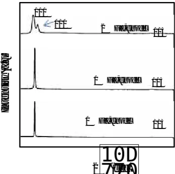
Fi. 1 shows the XRD spectrum for ZnO:Ga thin films at 1 and 3% Ga-doped concentration. The spectrum has been compared by ZnO:Ga (2%) XRD spectrum in the previous work [7]. As shown in Fig. 1, a strong (002) peak is observed at
2
= 34.4 and a weak (004) peak for all samples. These crystalline dimension along c-axisis 34.57, 34.44 and 34.05 for 1, 2 and 3 % Ga concentration respectively, as estimated by Scherer formula. These peaks indicate that the crystal structure almost independent of the Ga-doped concentration. Only the films deposited with 3% Ga-doped concentration showed a weak (101) peak. It reveal that all of the obtained ZnO thin films were polycrystalline with the hexagonal wurzite structure and had a preferred orientation with c-axis perpendicular to the substrates [8]. These films showed that no Ga2O3phase was found from the XRD patterns, which implies that Ga atoms substitute Zn atom in the hexagonal lattice or probably segregate to the non crystalline region and form Ga-O bond. Ma et al. [2] believed that much of Ga is able to ionize into Ga3+and
substitute Zn2+, so that it can contribute a free electron from each Ga atom.
002 101
3 % Ga-doped 004
2 % Ga-doped 004
1 % Ga-doped 004
[image:2.595.206.380.517.689.2]2 (deg)
240
As the deposition Ga concentration doped increases, the diffraction angle does not change significantly and the intensity of of the (002) peak becomes more intense and sharper at 2% Ga concentration. However, when the Ga concentration at 3 %, the intensity of the (002) peak becomes very weak, which can be indicated to degraded the crystallinity of the samples. This is could occur because the number of Ga nuclei increase during the deposition process so that the distribution of crystallities became more random [9]. Thus, the XRD pattern demonstrated that crystallinity of the film was improved with increasing Ga-doped concentration from 1 to 2%, but the peak (002) intensity of the samples deposited at 3% Ga-doped concentration significantly decreased with increasing Ga concentration.TABLE I
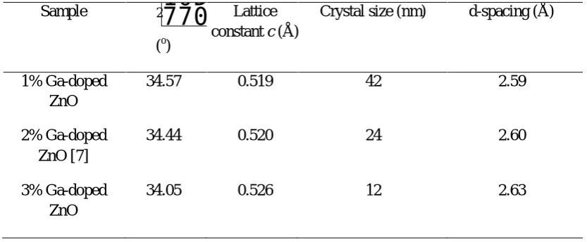
STRUCTURALPARAMETERS OFGALLIUMDOPEDZINCOXIDETHINFILMSDEPOSITED ATDIFFERENTARGON CONCENTRATION
Sample 2
(o)
Lattice constant c (Å)
Crystal size (nm) d-spacing (Å)
1% Ga-doped ZnO
34.57 0.519 42 2.59
2% Ga-doped ZnO [7]
34.44 0.520 24 2.60
3% Ga-doped ZnO
[image:3.595.96.513.237.409.2]34.05 0.526 12 2.63
Table I shows structural parameters of the ZnO:Ga thin films deposited. It clearly shown that the Ga concentration has a great influence on ZnO:Ga crystal size. These parameters reveal that increasing of the Ga- doped concentration reduces crystal size. However, the c-axis lattice constant, increased from 0.519 to 0.526 Å with increase in the Ga concentration. The increase in the c-axis lattice occurs probably due to the increase in substitution of Ga3+ions, so that increase the repulsive force total. Crystal size decrease from 42 to 12 nm with increasing Ga concentration showed that ion Ga3+more random distribution.
TABLE II
LATTICESTRAIN ANDSTRESSVALUE OFGALLIUMDOPEDZINCOXIDETHINFILMSDEPOSITED ATDIFFERENT ARGON CONCENTRATION
Sample Lattice strain Stress (GPa)
1% Ga-doped ZnO 0.1555 - 36.2234
2% Ga-doped ZnO 0.2068 - 48.2022
3% Ga-doped ZnO 0.5791 - 134.9198
241
filmfilm
4 tan
(1)Where
is lattice strain,
is full width half maximum (FWHM) and
is diffraction angle. Stress of the films is given by Eq.2.
XRD
233
(2) [image:4.595.224.402.308.389.2]Where
XRD denotes thin film stress.Fig. 2 shows the optical transmittance spectra for the ZnO:Ga thin films fabricated with 1 and 3% Ga-doped concentration. The spectrum of optical transmittance of the samples were compared with optical transmittance of ZnO:Ga (2%) spectrum also. The transmittance of the ZnO thin films with 1 and 2% Ga concentration were 85% in the visible region. This value is similar with the transmittance spectrum of the ITO thin films [5]. However, transmittance of 3% Ga-doped ZnO only reached about 70%. It occurs probably due to related with the degraded the crystallite structure of ZnO thin films.
ZnO Ga 1 % ZnO Ga 2 % ZnO Ga 3 %
Wavelength (nm)
Fig. 2. Transmittance spectrum of ZnO:Ga thin films prepared at different Ga-doped concentrations.
Energy (eV)
(a)
[image:4.595.163.377.474.771.2]242
g(b)
Energy (eV)
[image:5.595.167.377.56.220.2](c)
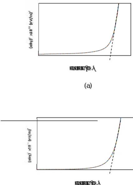
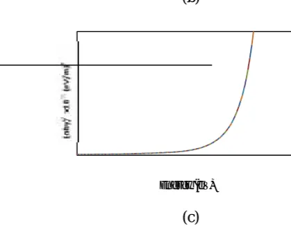
Fig. 3. Optical band gap (Eg) of ZnO thin films at different Ga-doped concentration: (a) 1%; (b) 2%; and (c) 3%.
ZnO:Ga thin films have a direct band gap, so that the absorption edge for interband transition is given by Eq. 3.
hv
2
A(hv
E )
(3)where
denotes the absorption coefficient and A denotes the constant for a direct transition. The Egof the filmsis obtained by plotting
2vs.hv
and extrapolating the straight line portion of this plot to the energy axis as shown in Fig. 4. As the Ga concentration increases from 1 to 3%, the band gap Eg of the ZnO:Ga thin films decrease from 3.28 to 3.22 eV, which is sorter than that of undoped ZnO (~3.3 eV) [5]. This deviation may be due to the structural defects takes place at deposition process [11]. The decrease of band gap occurs probably due to correlate with the crystal size and lattice strain of the films. Furthermore, the decreasing band gap can be due to the carrier concentration effect [12]. In previous work, Shin et al.[5] reported that the optical band gap would decrease with decreasing carrier concentration. On the other hand, Lin et al. [9] also reported that the carrier mobility dropped when Ga was between 3.0 and 10.0 at%IV. Conclusions
243
References
[1] J. Y. Kao, C. C. Tsao, M. Jou, W. S. Li, C. Y. Hsu,“Optimization of gallium-doped ZnO thin films grown using Grey-Taguchi technique,”J. Comput Electron., vol. 11 pp. 421-430, 2012.
[2] Quan-Bao, Zhi-Zhen Ye, Hai-Ping He, Li-Ping Zu, Bing-Hui Zhao, “Effects of deposition pressure on the properties of transparent conductive ZnO:Ga films prepared by DC reactive magnetron sputtering”,
Materials Science in Semiconductor Processing, vol. 10, 2007 pp. 167-172.
[3] S. Y. Lee, “Controllability of Structural, Optical and Electrical Properties of Ga doped ZnO Nanowires Synthesized by Physical Vapour Deposition”, Transactions on Electrical and Electronic Materials. Vpl. 14(3), 2013, pp. 148-151 .
[4] Ya Yang, Junjie Qi, Qingliang Liao, Yue Zhang, Xiaoqing Yan, Yunhua Huang, Lidan Tang,“Fabrication, structural characterization, and photoluminescence of Ga-doped ZnO nanobelts”, Appl. Phys. A, Vol 94, 2009, pp. 799-803.
[5] Hyun Ho Shin, Yang Hee Joung, Seong Jun Kang, “Influence of the substrate temperature on the optical and electrical properties of Ga-doped ZnO thin film fabricated by pulsed laser deposition”,J. Mater. Sci: Mater Electron, Vol 20, 2009, pp. 704-709.
[6] Y. Zhang, G. Du, D. Liu, X. Wang, Y. Ma, J. Wang, J. Yin, X. Yang, X. Hou, S. Yang, “Crystal growth of undoped ZnO films on Si substrates under different sputtering conditions”, Journal of Crystal Growth, Vol. 243, 2002, pp. 439-443.
[7] P. Marwoto, Fatiatun, B. Astuti, Sulhadi, D. Aryanto, and Sugianto, “Effects of Argon Pressure on the Properties of ZnO:Ga Thin Films Deposited by Dc Magnetron Sputtering”,Paper presented in the International Conference of Theoretical and Applied Physics (ITAP) 2014, Bali, Indonesia.
[8] X. Yu, J. Ma, F. Ji, Y. Wang, X Zhang, C. Cheng, H. Ma,“Influence of sputtering power on the properties of ZnO:Ga films deposited by r.f. sputtering at low temperature”, Journal of Crystal Growth, Vol. 274, 2005, pp. 474-479.
[9] Keh-moh Lin, Yu-Yu Chen, Chian-yuan Chiu, “Effects of growth behaviors on chemical and physical properties of sol-gel derived ZnO:Ga films”, J. Sol Gel Sci Technol, Vol. 55, 2010, pp. 299-305.
[10] M. Nayeef, W.Liaqut, S.Ali, &M.A.Shafique,“Synthesis of ZnO/Al:ZnO Nanomaterial: Structural And Band Gap Variation in ZnO nanomaterial by Al doping”, Applied Nanoscience,
[11] Li, Ying, Qin Huang, and Xiaofang Bi, “Stress Dependent Properties of Ga-Doped ZnO Thin Films Prepared by Magnetron Sputtering”,J. Mater, Sci.: Mater. Electron,, Vol. 24, 2013, pp.79–84.