Thesis by
Min Seok Jang
In Partial Fulfillment of the Requirements for the Degree of
Doctor of Philosophy
California Institute of Technology Pasadena, California
2013
c
2013
Acknowledgements
First, I would like to thank my advisor, Professor Harry Atwater. He always amazes me with his endless energy, enthusiasm, and knowledge. With his guidance, I have been able to experience diverse aspects of research throughout my graduate program. I especially thank him for giving me an opportunity to learn experiments at the end of my graduate studies.
Victor Brar has been a wonderful teacher for an experiment novice. He, Seyoon Kim, Josue Lopez and I have been working as a team on the graphene plasmonics project. I also thank Stanley Burgos for helping me to get accustomed to the Atwater group. He has been not only a good friend, but also a great mentor. It was my fortune to have worked alongside the inspiring young scientists in Atwater group.
Hyungjun Kim and I have been working on graphene electron optics more than three years. I still remember the days we discussed and wrote simulation codes in the Maui Wowi cafe. From my first year at Caltech, he has been my best friend and an amazing collaborator. I would also like to thank Professor William Goddard and Professor Young Woo Son for helpful discussions and comments.
I also thank my Korean friends who have kept my life enjoyable outside the lab— Chan Youn Park, Chang Soon Park, Jaewon Song, Hee Joong Chung, Junho Suh, Jeongwan Haah, Seokmin Jeon, Seung Ah Lee, Kun Woo Kim, Isaac Kim, Jeesoon Choi, Kiyoul Yang, Jeen Joo Kang, Hyoung Jun Ahn, Sonjong Hwang, and others.
I am grateful to Samsung Scholarship for financial assistance during my graduate study. I also thank Professor Frank Porter for offering numerous opportunities to serve as a teaching assistant for physics courses.
Mom and Dad for their endless supports. My little but bigger brother, Mooseok, you made my days at Caltech truly joyful. Thank you!
Min Seok Jang
November 2012
Abstract
The field of plasmonics has been attracting wide interest because it has provided routes to guide and localize light at nanoscales by utilizing metals as its major building block. Meanwhile, graphene, a two-dimensional lattice of carbon atoms, has been regarded as an ideal material for electronic applications owing to its remarkably high carrier mobility and superior thermal properties. Both research fields have been growing rapidly, but quite independently. However, a closer look reveals that there are actually numerous similarities between them, and it is possible to extract useful applications from these analogies. Even more interestingly, these research fields are recently overlapping to create a new field of research, namely graphene plasmonics.
Contents
Acknowledgements iii
Abstract v
1 Introduction 1
1.1 Plasmonics . . . 1
1.1.1 Drude Model of Metal . . . 2
1.1.2 Surface Plasmon Polaritons at a Metal-Dielectric Interface . . 3
1.1.3 Plasmonic Slab Waveguides . . . 5
1.2 Relativistic Electrons in Graphene . . . 8
1.2.1 Linear Dispersion Relation . . . 8
1.2.2 Massless Dirac Fermions . . . 13
1.2.3 Electron Optics in Graphene . . . 14
1.3 Graphene as a Tunable Plasmonic Material . . . 14
1.3.1 Optical Conductivity of Graphene . . . 15
1.3.2 Plasmons in Graphene . . . 17
1.4 Scope of This Thesis . . . 20
2 Plasmonic Dispersion Engineering: Trapped Rainbow in Tapered Plasmonic Waveguide 22 2.1 Introduction . . . 22
2.2 Transfer Matrix Analysis . . . 23
2.3 Mode Conversion Mechanism . . . 25
2.3.2 Mode Conversion in Rainbow Trapping Structures . . . 25
2.4 Performance of MIM Rainbow Tapers . . . 29
2.4.1 MIM TM2 Mode Trapping . . . 29
2.4.2 MIM TM1 Mode Trapping . . . 34
2.4.3 Trapped Rainbow in Real Materials . . . 34
2.5 Summary and Outlook . . . 35
3 Electron Optics in Graphene 37 3.1 Introduction . . . 37
3.2 Real-Time Numerical Simulation of Graphene Electrons: GraFDTD . 38 3.2.1 Finite-Difference Time Domain Method . . . 38
3.2.2 Excitation of an Electronic Gaussian Wavepacket . . . 40
3.3 Photonlike Behavior of Graphene Electron at a Heterojunction Interface 41 3.3.1 Snell’s Law . . . 42
3.3.2 Klein Tunneling . . . 44
3.3.3 Quantum Goos-H¨anchen Effect . . . 46
3.4 Electron Rainbow Trapping in Graphene . . . 48
3.4.1 Graphene Electron Waveguide . . . 48
3.4.2 Electron Rainbow Trapping . . . 50
3.5 Summary and Outlook . . . 53
4 Dispersion Engineering in Graphene: Graphene Field Effect Transistor without Energy Gap 55 4.1 Introduction . . . 56
4.2 Method . . . 57
4.2.1 GraFDTD Simulations . . . 57
4.2.2 Boundary Conditions . . . 57
4.2.3 Transmission Probability Calculation . . . 58
4.3 Electron Eigenmode Dispersion Relation . . . 58
4.4 Device Parameter Optimization . . . 62
4.6 Robustness Analysis . . . 67
4.6.1 Periodicity Perturbation . . . 67
4.6.2 Potential Blurring . . . 68
4.6.3 Finite Temperature . . . 69
4.7 Summary and Outlook . . . 70
5 Plasmonic Fano Resonance in Graphene Subwavelength Waveguide Modulator 71 5.1 Introduction . . . 71
5.2 Mode Conversion . . . 72
5.2.1 Eigenmode Field Profile . . . 73
5.2.2 Mode Conversion between MIM TM0 and Graphene Plasmon 75 5.3 Modulation Mechanism . . . 77
5.4 Device Parameter Dependence . . . 81
5.5 Carrier Mobility Dependence . . . 83
5.6 Summary and Outlook . . . 83
6 Graphene Nano Cavities at Near-Infrared Frequencies 85 6.1 Introduction . . . 85
6.2 Plasmon Resonance in Graphene Nanoribbons . . . 86
6.3 Graphene Ultrasmall Cavities at Telecommunication Frequencies . . . 89
6.3.1 Effect of Electron-Optical Phonon Interaction . . . 89
6.3.2 Near-Infrared Nano Bridge Cavity . . . 92
6.4 Graphene Resonator Arrays on SiO2 . . . 95
6.4.1 Sample Preparation and Measurement Methods . . . 95
6.4.2 Result and Discussion . . . 97
6.5 Summary and Outlook . . . 102
List of Figures
1.1 Dispersion relation and field profile of surface plasmon polaritons at a
metal-dielectric interface . . . 4
1.2 Dispersion relation and field profile of TM0 and TM1modes in MIM and IMI waveguides . . . 6
1.3 Atomic structure of graphene . . . 9
1.4 Unit cell and Brillouin zone of graphene . . . 10
1.5 Electronic band structure of graphene . . . 12
1.6 Optical conductivity of graphene . . . 15
1.7 Absorption spectra through a single layer graphene. . . 16
1.8 Field localization and propagation loss of graphene plasmons. . . 18
2.1 Waveguide discretization for transfer matrix calculation. . . 24
2.2 Mode conversion mechanism and eigenmode dispersion relation in vari-ous types of rainbow trapping structures . . . 26
2.3 Energy density distribution and mode amplitudes in IMI and MIM rain-bow trapping structures . . . 28
2.4 Broadband light trapping properties in a MIM tapered waveguide . . . 30
2.5 Taper angle dependence of quality factor Q and mode volume Veff . . 32
2.6 Magnetic field intensity distribution of TM1 and TM2 modes in MIM rainbow trapping structures . . . 33
3.1 Schematic of GraFDTD space discretization . . . 39
3.2 Snapshots of an electron wavepacket at a graphene heterojunction . . . 41
3.3 Reflection and refraction angles of an electron wavepacket at graphene heterojunctions . . . 43
3.4 Angle-dependent transmission and reflection probabilities of an electron wavepacket at graphene heterojunctions . . . 45
3.5 Quantum Goos-H¨anchen shift at graphene heterojunctions . . . 47
3.6 Electron eigenmode profile in graphene quantum well waveguides . . . 49
3.7 Dispersion relation of electron eigenmodes in graphene quantum well waveguide . . . 51
3.8 Electron rainbow trapping in graphene quantum well waveguides . . . 52
4.1 Schematic of sawtooth gate graphene FET . . . 59
4.2 Dispersion relation of electron eigenmodes and transmittance of a nor-mally incident electron plane wave in a sawtooth gate graphene FET . 61 4.3 Gate geometry optimization for a sawtooth gate graphene FET . . . . 63
4.4 Gate modulation and scaling behavior of a sawtooth gate graphene FET 64 4.5 Snapshots of an electron probability density profile in a sawtooth gate graphene FET at off state . . . 65
4.6 Transmittance of obliquely incident electron plane waves in a sawtooth gate graphene FET at off state . . . 66
4.7 Effect of periodicity perturbation on a sawtooth gate graphene FET . . 67
4.8 Effect of potential blurring on a sawtooth gate graphene FET . . . 68
4.9 Effect of finite temperature on a sawtooth gate graphene FET . . . 69
5.1 Schematic of graphene plasmonic waveguide modulator . . . 73
5.2 Field profiles of MIM TM0 and graphene plasmon modes . . . 74
5.3 Mode conversion between MIM TM0 and grpahene plasmon modes . . 76
5.4 Resonant transmission in graphene waveguide modulator . . . 78
5.5 Fano resonance in graphene waveguide modulator . . . 79
5.7 Carrier mobility dependence of modulation . . . 83
6.1 Phase shift of graphene plasmons upon reflection at the edges. . . 86
6.2 Plasmon resonance in free standing graphene nanoribbons . . . 88
6.3 Field localization and propagation loss of graphene plasmons . . . 90
6.4 Propagation loss of plasmons in graphene at high EF for various DC mobilities . . . 91
6.5 Fundamental mode of graphene nanobridge cavity . . . 93
6.6 Higher order modes of graphene nanobridge cavity . . . 94
6.7 AFM phase image of graphene nanocavity arrays . . . 96
6.8 Raman spectrum and electrical transport measurement of graphene on SiO2 . . . 96
6.9 Extinction spectra for polarizations perpendicular and parallel to ribbons 98 6.10 Extinction spectra of cavity arrays for various gate voltages . . . 99
6.11 Plasmon-phonon coupling of graphene on SiO2 . . . 100
Chapter 1
Introduction
The field of plasmonics and graphene electronics have been growing rapidly, but quite independently. However, a closer look reveals that there are actually numerous sim-ilarities between them, and it is one of the main purpose of this thesis to shed light on and extract useful applications from these analogies. Even more interestingly, these research fields are recently overlapping to create a new field of research, namely graphene plasmonics, which is the last topic of this thesis. In this chapter, we intro-duce basic concepts of plasmonics, and electronic and optical properties of graphene as bases for detailed discussions in the following chapters.
1.1
Plasmonics
In the past decade, the field of plasmonics has been attracting wide interest because it has provided routes to guide [52, 64, 83] and localize [23, 80, 98] light at scales substantially smaller than the free space wavelength. Unlike the conventional optics, plasmonics actively utilizes metals as its major building block. The interaction be-tween electromagnetic radiation and conduction electrons in metal induces distinctive, often counter intuitive, phenomenon such as negative refraction [12, 55, 88].
conventional optics.1
1.1.1
Drude Model of Metal
In the Drude model, conduction electrons in a metal form a free electron gas and move against fixed background ion cores [25]. When there is an oscillating external electric field E=E0e−iωt, the classical equation of motion for an electron becomes
dp
dt =−
p
τ −eE, (1.1)
wherepis the momentum of the electron. The relaxation time,τ, phenomenologically takes into account the electron scattering inside the metal. The Fourier transform of Eq. (1.1) yields
−iωp(ω) = −p(ω)
τ −eE(ω), (1.2)
p(ω) =−ieE(ω)
ω+i/τ =−
ieE(ω)
ω+iΓ. (1.3)
In the last step, the scattering rate Γ = 1/τ is introduced. The optical conductivity
σ(ω), which is the ratio of the current densityj =−nep/m to the electric field E, is given by
σ(ω) = j(ω) E(ω) =−
nep(ω)
mE(ω) =
ine2
m(ω+iΓ), (1.4) wheren,e, andmare the carrier density, the elementary charge, and the mass of the electron respectively. The relative permittivity of the metal (ω) is directly deduced from Eq. (1.4),
(ω) = 1 +iσ(ω) 0ω
= 1− ne
2
m0(ω2+iΓω)
= 1− ω
2 p
ω2+iΓω, (1.5)
1For more details on electronic and optical properties of metals, see Ref. [2]. Reference [65]
where ωp = ne2/m0 is the plasma frequency of the free electron gas. Note that, flips its sign at ω =ωp for small damping Γω.
It should be noted that the Drude description is valid even up to the ultraviolet for alkali metals, but for noble metals the model becomes inaccurate for high frequencies at which interband transitions occur. A more detailed review on the Drude model and the optical response of metals is given in Ref. [2].
1.1.2
Surface Plasmon Polaritons at a Metal-Dielectric
In-terface
A flat metal-dielectric interface supports SPPs at frequencies below the plasma fre-quency ωp (i.e., the metal has negative permittivity, Re{m} <0). The field profile and the dispersion relation of SPP can be obtained by solving the Maxwell’s equations [65]. Let us assign a coordinate system such that the x axis is perpendicular to the metal-dielectric interface (x = 0). We seek for transverse magnetic (TM) polarized guided mode propagating along the +z direction with a propagation constant β (the system does not support transverse electric (TE) polarized mode). We adopt the following ansatz for the magnetic field Hy(x, z),
Hy(x, z) =
A2eiβzeγ2x where x <0,
A1eiβze−γ1x where x >0,
(1.6)
where γi =
p
β2−k2
0i and k0 = ω/c is the free space wavevector. The expression for the electric field can be obtained from the sorce-less Maxwell’s equation E = (i/ω0)∇ ×H [84]. From the continuity of the magnetic field Hy and the in-plane component of electric field Ez, we get
A1 =A2, and (1.7)
β = ω
c
r
dm
d+m
0 0.5 1.0 1.5 2.0 0
0.2 0.4 0.6 0.8 1.0 1.2
-5 0 5 10 15
0 0.2 0.4 0.6 0.8 1.0
Real
Imaginary
a
[image:15.612.134.471.91.575.2]b
Figure 1.1: (a) Dispersion relation of SPPs at a metal-air interface. The scattering rate Γ is assumed to be negligible. The real part (red solid) and the imaginary part (blue dashed) of the normalized propagation constantβc/ωp are both presented. The black dotted line indicates the free space dispersion. Asωapproaches toωSP =ωp/
√
2, the group velocity vg = ∂ω/∂β of the SPP decreases. (b) Magnetic field profile of SPPs at ω = 0.5ωSP = 0.35ωp (red solid) and 0.8ωSP = 0.57ωp (blue dashed). As
Figure 1.1 (a) presents the dispersion relation of SPPs at an interface between the free space (d = 1) and a Drude a metal with negligible damping (Γ = 1). For
ω > ωp, the metal layer is transparent (i.e., m >0) and thus allows the propagation of unbound radiation. Note that the transverse decay constantγ becomes imaginary in this frequency regime. On the other hand, for ω < ωSP = ωp/
√
1 +d = ωp/
√
2, the interface supports a bound mode. The electromagnetic field in free space becomes more tightly confined near the interface as ω approaches to ωSP (Fig. 1.1 (b)). The group velocity vg = ∂ω/∂β vanishes and the surface plasmon resonance occurs at
ω =ωSP. The condition for the surface plasmon resonance is more generally written as
d+m = 0, (1.9)
which makes the denominator of Eq. (1.8) vanish. Between ωSP and ωp, β is purely imaginary, indicating there is no propagating mode.
1.1.3
Plasmonic Slab Waveguides
By putting two metal-insulator interfaces close together, we form symmetric and an-tisymmetric hybrid SPP modes. These modes are also referred to as TM0 and TM1 modes respectively, according to the number of zeros in their transverse field pro-file. For simplicity and clarity, we focus our discussion on two representative trilayer geometries: a metal/insulator/metal (MIM) and an insulator/metal/insulator (IMI) slab waveguides. We further assume that the structures possess a mirror symmetry with respect to x= 0 plane. Let the thickness of the core layer bed.
The magnetic field profile for the symmetric (Hs
0 1 2 3 4 5 0.0
0.2 0.4 0.6 0.8 1.0 1.2 1.4 0.0 0.2 0.4 0.6 0.8 1.0 1.2 1.4
M
I I
M I M
a
[image:17.612.135.452.106.591.2]b
Figure 1.2: Dispersion relations of TM0 (symmetric, blue solid) and TM1 (antisym-metric, red solid) modes in (a) MIM and (b) IMI waveguides. Lossless (Γ≈0) Drude dispersion is assumed for the metal layers. The thickness of the core is chosen as
modes are
Hys(x, z) =
Aeiβz cosh(γ1x)
cosh (γ1d/2)
where |x|< d
2,
Aeiβzexp
−γ2
|x| −d
2
where |x|> d
2,
(1.10)
Hya(x, z) =
Aeiβz sinh(γ1x) sinh (γ1d/2)
where|x|< d
2, sgn(x)Aeiβzexp
−γ2
|x| − d
2
where|x|> d
2,
(1.11)
where γi =
p
β2−k2
0i and β is the propagation constant. The boundary conditions atx=±d/2,Hy and Ez are continuous, yield the following dispersion relations.
tanh γ1 d 2
=−γ21
γ12
TM0 (Symmetric), (1.12) tanh γ1 d 2
=−γ12
γ21
TM1 (Antisymmetric), (1.13)
1 =d and 2 = m(ω) for the MIM waveguide, whereas 1 =m(ω) and 2 =d for the IMI waveguide.
from the other plasmonic modes (Fig. 1.2).
By bringing the interfaces into close proximity to each other, MIM TM1 modes and IMI TM0 modes exhibit negative group velocity, vg = ∂ω/∂β < 0, which is not observed for decoupled SPPs (Fig. 1.2). The negative group velocity arises from the fact that the direction of power flow in metal is opposite to that in dielectric materials, and the larger amount of power is conveyed in the metal layers. One can also interpret this phenomenon as a consequence of the negative Goos-H¨anchen shifts at metal-dielectric interfaces [37].
In Chapter 2 we discuss on a more exotic example of dispersion engineering on plas-monic waveguides. A MIM waveguide is also a major building block of the graphene-based plasmonic waveguide modulator, which is presented in Chapter 5.
1.2
Relativistic Electrons in Graphene
Graphene is a two-dimensional honeycomb lattice of carbon atoms. This two dimen-sional allotrope of carbon is mechanically very strong, showing a breaking strength that is 200 times greater than steel with a Youngs modulus of 0.5 TPa from atomic force microscope experiments [33]. Graphene also exhibits an extremely high thermal conductivity of ∼5×10³ W/mK [5]. Most importantly, graphene is a ballistic con-ductor exhibiting a remarkably high electron mobility exceeding 200,000 cm2V−1s−1 [10]. Therefore, it has been regarded as an ideal material for electronic applications. In this section, we discuss on the electronic properties of graphene. We describe the tight binding model of graphene and explain how the charge carriers in graphene have relativistic nature. We then briefly introduce the field of electron optics, and remark that graphene is an excellent system for electron optics.2
1.2.1
Linear Dispersion Relation
Atomistic structure of the graphene has a hexagonal lattice with two carbon atoms per cell interconnected through covalent bonds. Among four valence electrons of
orbital
bond
Figure 1.3: Graphene is a two-dimensional carbon allotrope forming a honeycomb lattice. Among four valence electrons of the carbon atom, three are used to make σ
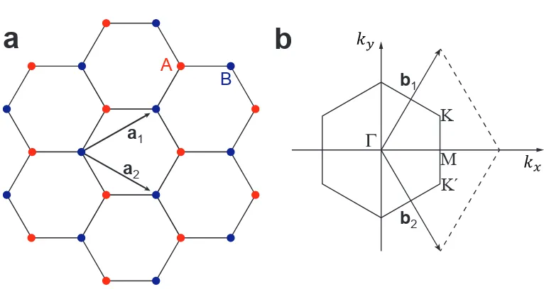
A B a1 a2 b1 b2
M
K
K `
a
b
Figure 1.4: (a) Graphene honeycomb lattice. Within a unit cell, there are two basis atoms called as sublattice A (red dots) and sublattice B (blue dots). a1 and a2 are
lattice unit vectors. (b) Brillouin zone with reciprocal lattice vectors of b1 and b2.
Three high-symmetry points in the reciprocal space (Γ, M, and K) are shown. each carbon, only three are involved in the covalent bonds (σ orbital) forming a honeycomb lattice while the other one is occupied in the orbital perpendicular to the graphene sheet (π orbital) as shown in Fig. 1.3 [13]. Many intriguing physical properties of the graphene are determined by the electrons near the Fermi energy of which wavefunction is composed of the linear combination of π orbitals. The lattice parameter of the graphene is given as
a1 =
3a 2 , √ 3a 2 !
, a2 =
3a
2 ,−
√
3a
2
!
, (1.14)
where a is the carbon-carbon distance of 1.42 ˚A(see Fig. 1.4(a)). This results a hexagonal shape of Brillouin zone (BZ) as shown in Fig. 1.4(b). Among the high symmetry points in BZ, two points located at the corners,KandK0are of importance, which are named as Dirac points. The momentum space positions of Dirac points are
K=
2π
3a,
2π
3√3a
, K0 =
2π
3a,−
2π
3√3a
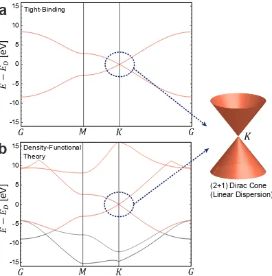
We assume that the electrons are tightly bound near the lattice points and can hop to nearest-neighbor sites, which is a realistic assumption because the overlap function between two π orbitals decays fast (compare Fig. 1.5(a) from nearest-neighbor hop-ping tight binding Hamiltonian and Fig. 1.5(b) from the density functional theory calculation). This leads a tight-binding Hamiltonian [13] of
H =−t X
hi,ji,σ
a†σ,ibσ,j + h.c.
, (1.16)
whereaσ,i(a †
σ,i) is an annihilation (creation) operator of electron with spinσ on site i of the sublattice A, and bσ,j(b
†
σ,j stands for the same operation on sitej of sublattice B (~ is set as unity for brevity). t is a nearest neighbor hopping energy which is around 2.8 eV. The bandstructure of the Hamiltonian (1.16)
E±(k) = ±t
v u u
t3 + 2 cos
√
3kya
+ 4 cos
√
3 2 kya
!
cos
3 2kxa
. (1.17) Electronic band of Eq. (1.17) is shown in Fig. 1.5(a). The energy value spectrum is symmetric around zero energy (meaning the electron-hole symmetry) and crosses at Dirac points. Eq. (1.17) can be expanded near Dirac points (Kand K0) with respect to the relative momentum vector q=k−K:
-15 -10 -5 0 5 10 15 -15 -10 -5 0 5 10 15
(2+1) Dirac Cone (Linear Dispersion) Tight-Binding
Density-Functional Theory
a
b
[e
V
]
[e
V
[image:23.612.109.505.151.553.2]]
1.2.2
Massless Dirac Fermions
To describe the linear dispersion relation, one requires a Dirac equation describing relativistic dynamics of spin 1/2 particle instead of a Schr¨odinger equation. The cone shaped energy band (Fig. 1.5) makes the effective mass to be zero. Thus the carrier electron dynamics becomes effectively identical to the (2+1)-dimensional quantum electrodynamics (QED). The expansion of the tight-binding Hamiltonian of Eq. (1.16) up to a linear order in nearest-neighbor vectors yields an effective Hamiltonian of
H ≈ −ivF
Z
dxdyhΨˆ†1(r)σ· ∇Ψˆ1(r) + ˆΨ † 2(r)σ
∗· ∇ˆ Ψ2(r)
i
, (1.19) where Pauli matrices σ = (σx, σy) and σ∗ = (σx,−σy), and ˆΨi = (ai, bi). Here, the subscript 1 and 2 denote theKand K0 points as shown in Fig. 1.4(b)) [13]. Thus, by introducing a electron wavefunction Ψ = (ψ1, ψ2) with two-(pseudo)spin components around theKpoint, the graphene electron wavefunction can be described by using a two-dimensional Dirac-like equation:
−ivFσ· ∇Ψ(r) =EΨ(r), (1.20) In momentum space, free graphene electron wavefunction Ψ(k) near Dirac points of K orK0 has the form of
Ψ±,K(k) =
1
√
2
e−iθk
±eiθk
, Ψ±,K0(k) =
1
√
2
eiθk
±e−iθk
. (1.21)
flips the momentum of the charge carrier from +k to −k should flip the direction of the pseudospin simultaneously, which is not possible if the Hamiltonian (1.19) is valid. This suppresses the backscattering of graphene carriers substantially, often referred to as Klein tunnelling [51], leading an extremely high carrier mobility.
1.2.3
Electron Optics in Graphene
Electronic analogues of optical behaviors such as focusing [90, 96, 102], collima-tion [72], and interference [108] have been achieved in two-dimensional electron gas (2DEG) systems. Bridging two fundamental physics, optics and electronics, has been made possible thanks to the ballistic transport properties of 2DEG. This has been cultivating new concepts for the manipulation of electrons in ways similar to that of photons in optical systems, which is referred as an “electron optics.”
Graphene, the ideal 2DEG, is the most suitable system for electron optics. It has a substantially large carrier mean free path as large as a few microns [10], yielding a robust ballistic transport regime. Additionally, the two basis atoms with 3-fold symmetry in the graphene unit cell result in a semimetallic electronic band effec-tively described by a (2+1) dimensional Dirac cone. Therefore, the quasiparticles in graphene share several relativistic properties with photons, described by a (3+1) dimensional Dirac cone, although those two are intrinsically different from each other (e.g., graphene electrons are charged fermions but photons are uncharged bosons).
In Chapter 3 and 4, we explore the similarities and differences in behaviors of relativistic electrons in graphene and electromagnetic waves in optical systems.
1.3
Graphene as a Tunable Plasmonic Material
0.0 0.5 1.0 1.5 2.0 2.5 3.0 3.5 -1.0
[image:26.612.125.467.61.326.2]0.0 1.0 2.0
Figure 1.6: Optical conductivity of graphene, in units σ0 = e2/4~, as a function of frequency ω. The real part (Re{σ}, red) and the imaginary part (Im{σ}, blue) are plotted for T /EF = 0.005 (solid) and 0.05 (dashed). The red shaded area denote the regime of interband excitations.
plasmon resonance of graphene nanoribbon arrays [46], and by acquiring their near field images [17, 32].
In this section, we focus on graphene as a plasmonic material. We discuss on the optical conductivity of graphene and then derive the properties of plasmons in graphene.3
1.3.1
Optical Conductivity of Graphene
The optical conductivity σ(ω) of graphene consists of the intraband σintra and the interbandσintercontributions. Neglecting the spatial dispersion,σintra andσintercan be analytically written as follows within the random phase approximation (RPA) [30, 31].
σintra(ω) =
e2ω iπ~
Z ∞
−∞
d|| ω2
df()
d =
2ie2T
π~(ω+iΓ)ln [2 cosh(EF/2T)], (1.22)
3References [30, 92] derives the AC electrical conductivity of graphene. A more detailed discussion
0.2 0.4 0.6 0.8 1.0 1.2 0.0
0.5 1.0 1.5 2.0
[%]
a
b
[image:27.612.97.511.70.312.2][eV]
Figure 1.7: (a) Schematic of a transmission measurement through a single layer graphene. (b) Numerically simulated spectra 1−T for EF = 0.01eV (red solid), 0.2eV (blue dashed), and 0.4eV (green dotted), assuming room temperature. Note that the absorption abruptly increases atω = 2EF and becomes constant(∼πe2/~c) for higher photon energies, as a result of interband transitions.
σinter(ω) = ie 2ω
π~
Z ∞
0
d f(−)−f()
(ω+iδ)2−42, (1.23) where f() = 1/(exp[(−EF)/T] + 1) is the Fermi distribution function, and Γ is the scattering rate of carriers. More general expression for the conductivity tensor with non-negligible spatial dispersion is given in Ref. [30]. In low temperature limit,
T EF, σintra recovers the Drude from,
σintra(ω) =
ie2|EF|
π~(ω+iΓ). (1.24)
σinter is also further reduced, yielding
σinter(ω) =
e2
4~
θ(ω−2EF)−
i πln
ω+ 2EF
ω−2EF
, (1.25)
The real part of the conductivity shows a step at ω = 2EF, which corresponds to the onset of the interband transition (Fig. 1.6). In other words, when ω >2EF, the optical loss in graphene is dominated by the interband transition. As an interesting consequence, the optical transmittance of a free-standing graphene also has a step at
ω ≈2EF and becomes flat for higher frequencies (Fig. 1.7). The optical transmittance atω > 2EF can be analytically expressed as [54]
Topt =
1 + πe 2
2~c
−2
≈1− πe
2
~c ≈0.977. (1.26) For ω < 2EF, the optical loss in graphene is determined by various electron scattering processes. Electron-impurity scattering dominates at low frequencies, and the scattering rate Γimp can be estimated from DC mobility µ, such as Γimp =
e~vF2/µEF. Electron-optical phonon scattering becomes significant above the phonon energy ωph∼0.2eV [41].
1.3.2
Plasmons in Graphene
A layer of graphene supports plasmons. Similar to Section 1.1.2, we obtain the field profile and the dispersion relation of graphene plasmons by solving the Maxwell’s equations. Here we consider TM modes in graphene, which lies on x = 0 plane, sandwiched by dielectric media of permittivity 1 and 2.4 We again use Eq. (1.6) as the ansatz for the magnetic field Hy(x, z). The boundary condition, however, is quite different, because there is a sheet currentσEz flowing along the graphene layer, which induces a discontinuity in the magnetic field.
Ez x→0+
=Ez x→0−
, (1.27)
Hy x→0+
−Hy x→0−
=σEz(x= 0). (1.28)
4Graphene also supports TE modes at 1.667< ω/E
0 50 100 150 200
0 0.05 0.10 0.15 0.20
0 5 10 15 20
-0.10 -0.05 0.00 0.05 0.10
[eV]
a
[image:29.612.129.459.138.581.2]b
Figure 1.8: (a) Field localization Re{β}/k0 and (b) normalized propagation loss Re{β}/Im{β} of plasmons in a suspended graphene (1 =2 = 1) for EF = 0.16eV,
The dispersion relation for graphene plasmons is then analytically written as
1
p
β2 − 1k20
+ p 2
β2− 2k20
=−i σ ω0
. (1.29)
In non-retarded regime (β ω/c), the above equation is further simplified, yield-ing
β ≈i(1+2)0ω
σ . (1.30)
At frequencies much lower than the interband threshold yet much higher than the scattering rate (Γ ω 2EF), σ is inversely proportional to ω (see Eq. (1.24)). The dispersion relation for low energy plasmons is thus β ∝ω/σ ∝ ω2, or ω ∝ √β. Note that the low energy dispersion of SPPs on metals is ω ∝ β (Fig. 1.1). This qualitative difference is originated from the differences in electronic dispersions— linear for graphene and quadratic for bulk metals.
Figure 1.8 plots the field localization and the normalized propagation loss of plas-mons in a suspended graphene (1 = 2 = 1) as a function of frequency, assuming
EF = 0.16eV, T = 300K, and Γ = 4.1meV, which corresponds to the mobility of 104cm2V−1s−1 [74]. The field confinement factor is calculated to be around 30–100 with reasonable losses Re{β}/Im{β} >10. From Eq. (1.30), we know that the field localization can be readily enhanced by factor of (1 +d)/2 by placing graphene on a dielectric substrate of permittivity ofd. The effect of interband transition become significant for high frequencies, resulting in substantial propagation losses. By increas-ing EF, it is possible to achieve much longer propagation lengths, Re{β}/Im{β} 100 [41]. The mobility of 104cm2V−1s−1 can be improved by employing hexagonal boron nitride substrates, even up to 106cm2V−1s−1 [21, 66]. This may further reduces the plasmon losses.
1.4
Scope of This Thesis
This thesis discusses five interrelated topics on plasmonic dispersion engineering, graphene electron optics, and graphene plasmonics. The chapters are organized as follows:
Braodband Slow Light in Tapered Plasmonic Waveguide
As an example of plasmonic dispersion engineering, Chatper 2 describes “rainbow trapping” structures, which has been proposed as a scheme for localized storage of broadband electromagnetic radiation in metamaterials and plasmonic heterostruc-tures. We articulate the dispersion and power flow characteristics of rainbow trapping structures, and show that tapered waveguide structures composed of dielectric core and metal cladding are best suited for light trapping. A metal/insulator/metal taper acts as a cascade of optical cavities with different resonant frequencies, exhibiting a large quality factor and small effective volume comparable to conventional plasmonic resonators.
Electron Optics in Graphene
Chapter 3 presents a few examples of electron optics in graphene. We investigate the temporal behavior of a single localized electron wavepacket, showing that it exhibits optics-like dynamics including the Goos-H¨anchen effect at a heterojunction and the Rainbow trapping effect in a tapered electron waveguide, but the behavior is quanti-tatively different than for electromagnetic waves. To study the dynamics of graphene electrons numerically, we develop a finite difference time domain (FDTD) method for simulating the dynamics of graphene electrons, denoted GraFDTD.
Graphene Field Effect Transistor without Energy Gap
dispersion of electron eigenmodes in a Kronig-Penney potential. A major complica-tion in realizing graphene based field effect transistors for logic applicacomplica-tions is that the electrons in pristine graphene exhibit unimpeded Klein tunnelling through gate potential barriers. Introducing a band gap in graphene suppresses Klein tunnelling, but inevitably degrades the carrier mobility. To solve this dilemma, we propose a gating mechanism employing a sawtooth-shaped gate potential geometry (in place of the conventional bar-shaped geometry) that leads to a hundredfold enhancement in on/off transmission ratio for normally incident electrons without any band gap engineering.
Graphene Subwavelength Waveguide Modulator
Chapter 5 presents a scheme for modulating mid-infrared transmission of plasmonic waveguides by employing the Fano interference between transmission through plas-mon resonance in graphene and nonresonant background transmission. We deplas-mon- demon-strate that the overall transmission can be almost completely suppressed by total destructive interference, which is ideal for switching applications. Because of the high field confinement of graphene plasmons, the effective volume of the structure is much smaller than the free space wavelength.
Graphene Nano Cavities at Near-Infrared Frequencies
Chapter 2
Plasmonic Dispersion Engineering:
Trapped Rainbow in Tapered
Plasmonic Waveguide
“Rainbow trapping” has been proposed as a scheme for localized storage of broadband electromagnetic radiation in metamaterials and plasmonic heterostructures. Here, we articulate the dispersion and power flow characteristics of rainbow trapping struc-tures, and show that tapered waveguide structures composed of dielectric core and metal cladding are best suited for light trapping. A metal/insulator/metal taper acts as a cascade of optical cavities with different resonant frequencies, exhibiting a large quality factor and small effective volume comparable to conventional plasmonic resonators.1
2.1
Introduction
Slow electromagnetic waves, first studied in systems with atomic coherence at low temperature [59], have been investigated in recent years at room temperature via light dispersion in solid state media such as photonic crystals [34, 104]. However most of these systems operate only at specific resonant frequencies, and so broadband light trapping remains a great challenge. Tsakmakidis et al. first proposed “rainbow trapping” in which a wide wavelength range of electromagnetic fields can be trapped in
tapered waveguide structures composed of negative index core and dielectric cladding (insulator-negative index-insulator, or INI) that exhibits a negative Goos-H¨anchen effect [98]. Recently, researchers have determined that such trapping mechanism is also applicable for transverse magnetic (TM) waves in insulator-metal-insulator (IMI) and metal-insulator-metal (MIM) waveguide tapers under certain material property conditions [63, 79]. However, to date the question of how much light a rainbow trapping structure can actually store and how the light escapes from it has not been addressed.
In this work, we study fundamental mode conversion and loss mechanisms of linearly-tapered INI, IMI, and MIM rainbow trapping structures and show that MIM rainbow trapping structures are superior to the others in terms of trapping perfor-mance. Assuming a Drude dispersion relation for the cladding metal, we specify the frequency range and the structural dimensions needed to achieve rainbow trapping and calculate the quality factor Q and the effective mode area Aeff as quantitative measures of light trapping and localization. We perform a transfer matrix analysis [110] to examine the behavior of the guided modes in the structure, and confirm the results with full-wave finite difference time domain (FDTD) and finite element method (FEM) simulations. This chapter is organized as follows: Fig. 2.2 illustrates the mode conversion properties of IMI, INI and MIM tapers. We then compare the energy density distributions and modal amplitudes achievable for IMI TM0 modes and MIM TM2 modes, as indicated in Fig. 2.3. For MIM tapers, we then investigate the critical taper thickness for mode conversion and the quality factor achievable for the quasi-bound mode as a function of frequency. Finally we explore the properties of rainbow tapers as a function of taper angle, as illustrated by Fig. 2.5.
2.2
Transfer Matrix Analysis
0
1
2
3
⋯
Δ
= /
Figure 2.1: Waveguide discretization for transfer matrix calculation.
the modes are partially transmitted and partially reflected. We can analytically obtain the coupling coefficients from the field continuity conditions and the orthogonality relations. This can be conveniently expressed in matrix form, aj+1 =SjTjaj. Here, aj =
ajf+, ajf−, ajb+, ajb− the vector whose elements are the mode amplitudes in j-th waveguide segment, andTj andSj are 4×4 transfer matrices,respectively describing the propagation of the modes in the segment and the intermode coupling at the interface between j-th and (j+ 1)-th segments.
Tjlm=δlmexp (ik0nl∆z), (2.1) Sjlm=
R
ej+1l ×hj m
z +
R
ej m×h
j+1 l
z 2R ejm×hjm
z
, (2.2)
where e and h are the vector waveguide modes such that E = ae and H = ah. Expanding this argument to the entire series of waveguide segments, the mode am-plitudes of the taper ends are related by
aN = N
Y
j=1
SjTja1. (2.3)
The mode amplitudes are normalized such that |a|2 = |R
modes having real propagation constants,|a|2 is simply the time-averaged power flow.
2.3
Mode Conversion Mechanism
2.3.1
Dispersion Relation of Guided Modes
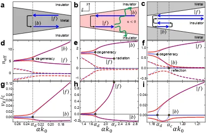
The dispersion relations of eigenmodes in rainbow trapping systems are exotic. Fig-ures 2.2(d)–(f), respectively, show the effective indices neff of IMI TM0 modes and modes in INI and MIM tapers as a function of core thickness α. For all three cases, the modes consist of two branches; the energy velocity,
vE =
R
Szdx
R
udx , (2.4)
where u and S are the time averaged energy density [85] and Poynting vector, and the phase velocity are parallel for one branch (|fi) and antiparallel for the other (|bi), as seen in Figs. 2.2(g)–(i). Since each mode can propagate along either the +z or−z
direction, there exist a total of four orthogonal eigenmodes|f+i,|f−i,|b+iand|b−i. The letters f and b identify the branch and the signs + and −indicate the direction of energy propagation. If the system is adiabatic enough to neglect the coupling between these modes and higher order modes, it is possible to describe the system as a linear superposition of these four basis modes. The |fi and |bi are degenerate at a certain core thickness, αd, and the dispersion relations splits as α deviates from αd. It is worth noting that the direction of power flow through the cladding is opposite to the flow through the core and their magnitudes become equal atα=αdwhich results in zero energy velocity. The conditions for having degeneracy points are specified in Table 2.1 [63, 79].
2.3.2
Mode Conversion in Rainbow Trapping Structures
1.18 1.20 1.21 0.00 0.02 0.04 -0.5 0.0 0.5 1.0 0 5 10 0.18 0.20 0.22 0.26 0.00 0.02 0.04 0.06 0.08 0.10 degeneracy degeneracy reflection Insulator Metal Insulator
a
b
c
d
g
e
h
f
i
Metal Insulator Metal [image:37.612.99.517.194.463.2]1.4 1.6 2.0 2.4 2.6 2.8 -0.2 0.0 0.2 0.4 0.6 0.8 -1 0 1 2 degeneracy radiation Insulator Insulator 0.12 0.24
Figure 2.2: Schematic descriptions of (a)–(c) mode conversion mechanism, (d)–(f)
INI, NIN MIM IMI
TM0: σ >max{1, σµ−1} TM1: 1 < σ<1.13510 TM0: σ >1 TM1: 1< σ < σµ−1 TMm≥2: σ
−1/2
+ atan(σ−1/2)> mπ/2 TMm≥2: σσµ <1
Table 2.1: The conditions for rainbow trapping. σ =|II/I|and σµ =|µII/µI|where the subscripts I and II denote the core and the cladding respectively. For INI TE modes, replace σ↔σµ .
from the coupling between the eigenmodes due to the fundamental nonadiabaticity near α = αd. More specifically, the slow core thickness variation condition [93],
dα/dz αk0∆n/π, where k0 is the wavenumber in the free space and ∆n is the effective index difference between eigenmodes, can never be fulfilled throughout the entire structure because ∆n = 0 at the degeneracy point. In fact, the degeneracy point connects |f±i to |b∓i. Mechanisms for power flow into and out of rainbow trapping structures are schematically described in Figs. 2.2(a)–(c). An incident IMI TM0 |f+iis converted to the other branch|b−iatα=αdand escapes the structure. In an INI structure, an incident photonic |b+i is converted to |f−i at α = αd and couples into a backward propagating radiative mode at α =αr, where neff coincides with the index of the cladding. An incident MIM photonic |f+i undergoes similar mode conversion at the degeneracy point but the converted |b−i is reflected to |b+i
at the mode cutoff α = αc, and converted back to |f−i, which finally escapes the structure. The reflection at α = αc, where the energy velocity also vanishes, makes electromagnetic waves reside longer in the taper segment between the degeneracy point and the mode cutoff.
1.14 1.16 1.20 1.22 1.24 1.26 0.0 0.2 0.4 0.6 0.8 1.0 1.2 M od e Amplitude 0.0 2.5 2.5 0 Metal Insulator Metal 0.14 0.16 0.18 0.20 0.22 0.26 0.0 0.2 0.4 0.6 0.8 1.0 M od e Amplitude 0.0 -0.5 0.5 Metal Insulator Insulator
a
b
[image:39.612.107.504.75.295.2]c
1.2d
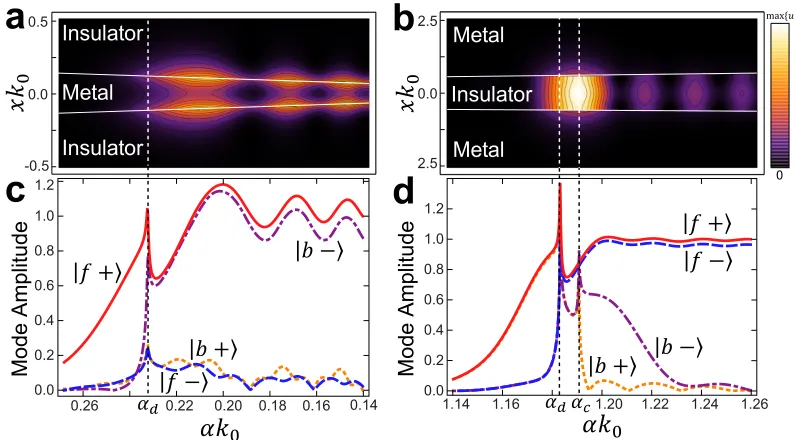
Figure 2.3: Energy density distributionu(x, z) of (a) IMI (I =−8.5,II= 10 + 0.01i) TM0 and (b) MIM (I = 10,II=−1 + 0.001i) TM2 modes. Boundaries between core and claddings are indicated by white solid lines. (c),(d) Mode amplitudes of |f+i
(red solid), |f−i (blue dashed), |b+i (orange dotted), and|b−i (purple dash-dotted) modes as functions of core thickness in the (c) IMI and (d) MIM structures. Dotted vertical lines indicate αd and αc.
consecutive Goos-H¨anchen shifted internal reflections also decreases, crosses zero, and becomes negative which corresponds to our mode conversion description at α = αd. For INI structures, the light ray escapes the structure in the form of radiation once ΘN reaches the angle of escape Θr determined by Snell’s law (Fig. 2.2(b)). Therefore a ray can bounce M times, where M is the largest integer satisfying ΘM >Θr (i.e.,
M ∼ (Θ0 −Θr)/θ). On the other hand, in MIM structures, the light ray is always totally reflected at the interface. Therefore ΘN can be further reduced and cross zero at the mode cutoff (α=αc) (Fig. 2.2(c)). From there, the ray travels back in the +z direction again and then repeats the same process that we described previously but in the reverse manner. The number of internal reflections is thus M ∼2Θ0/θ, which is greater than that of the INI case.
modes in the steady state. Corresponding to our previous description, af+ and ab− are of similar magnitude whereas af− and ab+ are very small, which indicates mode conversion from |f+i to |b−i, with other modes suppressed. On the other hand, for MIM TM2 mode trapping, |af+| ∼ |af−| where α > αc and |b+i and |b−i are excited only in the taper section α ∈ (αd, αc) and decay as they become evanescent (Fig. 2.3(d)). Due to the simultaneous excitation of |f+i, |f−i, |b+i and |b−i, an MIM structure can store large amounts of energy which makes them the best candidates for trapping light. Although an IMI structure can perform as a compact mode converter, its light trapping capability is inferior to the MIM trapping structure because it does not exhibit mode cutoff (Figs. 2.3(a) and (b)). Due to the inevitable radiation loss, in addition to the difficulties in fabrication, INI rainbow trapping seems less attractive compared to the other approaches. Therefore, we focus our attention on MIM rainbow trapping in the rest of the discussion.
2.4
Performance of MIM Rainbow Tapers
2.4.1
MIM TM
2Mode Trapping
Although rainbow trapping structures are open systems, they can be considered as a series of optical cavities having different resonant frequencies since they can local-ize broadband light in tapered sections of different width depending on frequency. Assuming a dispersionless dielectric core and a Drude metal cladding of
II= 1−
ω2 p
ω2+iΓω, (2.5)
where ωp and Γ are the plasma frequency and the damping constant respectively, TM2 modes at frequency
ω ωp
∈ (0.2430I+ 1)−1/2,1
0.27 0.28 0.29 0.30 0.0
0.2 0.4 0.6 0.8 1.0
0.6 0.7 0.8 0.9 1.0
0.0 0.2 0.4 0.6 0.8 1.0 1.2
0 5 10 15 20
0.0 0.1 0.2 0.3 0.4 0.5 0.6
II
ε
I
ε
a
b
c
104d
103
102
101
103
102
101
Figure 2.4: αd(blue dashed),αc−αd(blue dotted, 100 times magnified in (b)) andnd, the effective phase index of the mode at α =αd (red solid) of MIM (I= 10, θ = 2◦) (a) TM1 and (b) TM2 modes versus ω/ωp. αd and αc are normalized byk−1p =c/ωp. The inset in (a) shows the schematic of a MIM rainbow trapping structure. Qversus
can be trapped in the structure (Table 2.1). We plot αd, αc and nd as functions ofω in Fig. 2.4(b). As a measure of trapping performance, we calculate the quality factor
Q from electric and magnetic field distribution in the steady state. Q is defined by
Q=ωU
P, (2.7)
where P is the power dissipated and U is the energy stored in the rainbow trapping structure (z > 0) having the entrance thickness α0 (see inset of Fig. 2.4(a)). Here,
α0 is chosen to be max{αc(ω)} to ensure the structure to be functional for the entire target frequency range. Recognizing that the input power is equal to the dissipated power in steady state, and that the only incoming guided mode at the entrance (z = 0) is |f+i, P is equal to the incoming power carried by |f+i. Since the wave propagates deeper along the taper, Q increases asω increases for a fixed taper angle
θ = 2◦ (Fig. 2.4(d)). It is worth noting that Q is directly proportional to the light trapping timeτ =Q/ω. For instance, forθ = 2◦ andω/ωp = 0.6,τ is calculated to be around 33 periods, which is quite a long time since the distance between the entrance and the degeneracy point is only about 1.5 effective wavelengths. We confirm that
τ corresponds to the actual signal trapping time by measuring the time it takes by a pulse to escape a rainbow trapping structure by FDTD simulations. Interestingly, the signal trapping time does not vary significantly from the value of the lossless case but only causes the outgoing signal to attenuate as Γ becomes larger.
When material loss is present (Γ 6= 0), the degeneracy between |fi and |bi is removed and vE thus has finite value everywhere (Fig. 2.2(f)). However, the overall power flow and optical dispersion characteristics vE drops down significantly and that the effective indices of |fi and |bi get very close to each other around α = αd are preserved. Thus the previously described light trapping mechanism is still valid except at very high loss. For a fixed frequency, Q is found to be almost inversely proportional to the taper angle. As θ → 0, Q becomes limited by ohmic loss inside the metal alone, asymptotically approaching c/2vEIm{nefff+(α=α0)}(Fig. 2.5(b)).
0 0.2 0.4 0.6 0.8 1.0
0.5 1.0 1.5 2.0
0 0.4 0.8 1.2
0.5 1.0 1.5 2.0 0
1.0 2.0
0.5 1.0 1.5 2.0 0
1.0 2.0
[degree-1]
0 0.2 0.4 0.6 0.8
0.5 1.0 1.5 2.0
0 0.4 0.8 1.2
[degree-1]
a
b
[image:43.612.116.500.68.292.2]c
d
Figure 2.5: Qand Q/Veff versusθ−1 of (a), (c) MIM (I = 10) TM1 modes at ω/ωp = 0.277 for Γ/ωp = {0(red circles), 0.001(blue squares), 0.01(orange triangles)} and (b),(d) TM2 modes at ω/ωp = 0.6 for Γ/ωp ={0(red circles), 0.01(orange triangles), 0.1(purple diamonds)}. The insets in (a) and (c), respectively, plot Q and Q/Veff for Γ = 0 in full range. Q/Veff is normalized by (λ0/nI)−3.
structure as a measure of light localization, Aeff =U/max{u(x, z)}, where (x, z) re-side in the dielectric core where an object may be placed to interact with the eld. By conservatively assuming a diffraction-limited height Ly = λ0/2nI, the effective volume can be approximated as Veff ∼ Aeffλ0/2nI. Figure 2.5(d) displays Q/Veff of TM2 modes as a function of inverse angle θ−1. When Γ = 0, Q/Veff monotonically increases since adiabatic condition holds up toαcloser toαdasθ gets smaller. In the presence of material loss, the effect of rainbow trapping and propagation losses com-pete. TheQ/Veff is dominated by propagation loss for very small taper angle whereas the rainbow trapping effect dominates it for relatively large θ, because propagation loss exponentially increases as a function of propagation distance. Therefore Q/Veff has a maximum where both effects are balanced. For greater values of Γ, the optimal
TM
1
TM
2
2.4.2
MIM TM
1Mode Trapping
We note that TM1 modes at
ω ωp
∈ (1.3510I+ 1)−1/2,(I+ 1)−1/2
(2.8)
can also be trapped in the MIM taper structures. The parametersαd and αr of TM1 modes have similar order of magnitude to those TM2 modes, implying that both type of modes can be trapped in a single structure (Fig. 2.4(a)). However, unlike TM2 or higher-order photonic modes, TM1 modes are mostly antisymmetric super-positions of surface plasmon polariton modes. Their field intensity is greatest at the metal/dielectric interfaces and exponentially decays as a function of distance from the interface, making them slow compared to the photonic modes and very sensitive to changes at the vicinity of the surface. Because of the small energy velocity, Q of TM1 modes tends to be much higher than that of photonic modes and even diverges when ω approaches to surface plasmon resonance frequency if the metals are lossless (Fig. 2.4(c)). Moreover, since the energy of TM1 modes is highly confined at the interfaces, they can have very smallAeff well below the diffraction limit (Fig. 2.5(c)). However, because of the significant energy penetration into the metal, TM1 modes are much sensitive to the material loss than TM2 modes, making it difficult for them to exhibit a rainbow trapping effect for the realistic damping constant Γ/ωp ∼ 0.01 [45]. They also undergo nonnegligible reflection due to the tapering. This adds dis-tinctive Fabry-Perot type oscillations as a function of the taper length, as illustrated in Figs. 2.5(a) and (c). The TM1 modes might not be suitable for signal processing since the shape of a signal can be significantly distorted by this reflection.
2.4.3
Trapped Rainbow in Real Materials
a
b
Wavelength [nm]
Wavelength [nm]
550 560 570 580 5900.02 0.04 0.06 0.08
550 560 570 580 590 0
10 20 30 40 50 60
0
Figure 2.7: (a) Q and (b) Aeff of TM1 modes in a Ag/GaP/Ag rainbow trapping structure as functions of free space wavelength. Forα= 50 nm andθ = 5◦, we obtain
Q∼30–60 and Aeff ∼0.01–0.1 throughout the target wavelength range. As the exci-tation wavelength approaches the surface plasmon resonance wavelength (∼540 nm), the mode becomes highly lossy and more confined near Ag/GaP interfaces. In this regime, the system is dominated by propagation loss rather than the effect of rainbow trapping. Therefore, smallAeff near the surface plasmon resonance wavelength is not the direct consequence of the rainbow trapping effect. Aeff is normalized by (λ0/nI)2. the optical frequency range, MIM rainbow tapers with Ag [45] as the metallic layer and GaP [75] as the dielectric are able to trap TM1 modes for wavelengths ranging from 540 to 590 nm at α of 22–48 nm. For a Ag/GaP/Ag taper of α0 = 50 nm and
θ = 5◦, we obtain Q ∼ 30–60 and Aeff(λ0/nI)−2 ∼ 0.01–0.1 throughout the target wavelength range (Fig. 2.7). One could also trap infrared light by utilizing polar dispersive materials that support phonon-polariton modes as negative permittivity claddings. For instance, SiC/Si/SiC heterostructures are able to localize TM2 modes in infrared regime near the SiC phonon polariton resonance (∼10.5 µm) where the permittivity of SiC varies from positive to negative with very small damping [97].
2.5
Summary and Outlook
Figure 2.8: Schematic of an arrayed rainbow trapping structure for photovoltaic ap-plications. The structure traps different frequency bands of the solar spectrum into semiconductors of different band gaps arrayed along the taper in order to maximize the solar absorption.
Chapter 3
Electron Optics in Graphene
We develop a finite difference time domain (FDTD) method for simulating the dynam-ics of graphene electrons, denoted GraFDTD. We then use GraFDTD to study the temporal behavior of a single localized electron wavepacket, showing that it exhibits optical-like dynamics including the Goos-H¨anchen effect [37] at a heterojunction and the Rainbow trapping effect [98] in a tapered electron waveguide, but the behavior is quantitatively different than for electromagnetic waves. This suggests issues that must be addressed in designing graphene-based electronic devices analogous to opti-cal devices. GraFDTD should be useful for studying such complex time-dependent behavior of quasi-particle in graphene.1
3.1
Introduction
The graphene two-dimensional (2D) carbon material has two π electrons and two atoms per unit cell, resulting a semimetallic electronic band with a conical intersection at the Fermi energy (the K point of the Brillouin Zone). Thus charge carriers near the Fermi energy behave like 2D massless relativistic particles exhibiting a linear (photonlike) dispersion relation, which is effectively described by the Dirac equation with Fermi velocity vF ≈106 m/s [13]
h
−i~vFσ·∇~ +U
i
Ψ =i~∂Ψ
∂t, (3.1)
where U is the external electric potential, and σ = (σx, σy) are the Pauli matrices. This enables an analogy between the quantum wave nature of graphene electronics and the electromagnetic (EM) waves in dielectrics described by Maxwell equations within the electron mean free path scale. For example, graphene electrons can ex-hibit electronic left-handed materials [15], quantum Goos-H¨anchen (GH) shift [7, 113], Bragg reflectors [35], and wave guides [114]. All previous theoretical studies of these properties for graphene were carried out analytically, limiting the analysis to sta-tionary solutions such as finding confined modes [81, 114] or describing plane waves [7, 15, 35, 47, 113]. Such descriptions do not provide an understanding of the dynam-ics oflocalized electron wavepackets, which can be essential in tracing the position of the electron.
This chapter addresses the following questions: (1) Do the optical-like behavior formulated in the wave-like point of view of the graphene electron remains valid when one includes the particle-like character of spatially localized electron wave packets? (2) Can the graphene electron’s exotic tunneling behavior (Klein tunneling) or the GH shift be observed in the time-resolved dynamics? In order to clarify such questions, we developed the “GraFDTD” method to calculate numerically the time evolution of the de Broglie wave for the excited graphene electrons. In this chapter, we use GraFDTD to investigate the scattering behavior of an electron wavepacket at a heterojunction boundary. Then we study the rainbow trapping effect in a tapered electron waveguide, which is made of symmetric quantum well with varying width. We also compare our results with the dynamics of EM waves in the corresponding optical systems.
3.2
Real-Time Numerical Simulation of Graphene
Electrons: GraFDTD
3.2.1
Finite-Difference Time Domain Method
1
is assigned
2is assigned
Figure 3.1: Schematic of GraFDTD space discretization. Graphene is represented as a (M×N) rectangular grid with the pseudospin components ofψ1 andψ2 alternatively assigned on the grid points due to the symmetric shape of the update scheme. The external potential U(x, y) is applied on each grid point. An electron wavepacket is excited from the y= 0 boundary, and then propagates along +y direction.
evolution of Eq. (3.1), we discretize the time domain using the velocity Verlet algo-rithm, which has the virtue that it is a second order simplectic integrator allowing us to sample both ψ1 and ψ2 simultaneously. The update of Ψ = (ψ1, ψ2) during the time step ∆t is carried out via the following three steps:
1. Update of ψ1(t+ ∆t/2) from ψ1(t) and ψ2(t),
ψ1
t+∆t 2
=
1−iU∆t
2~
ψ1(t)−
vF∆t
2 (∂x−i∂y)ψ2(t). (3.2) 2. Update of ψ2(t+ ∆t) from ψ1(t+ ∆t/2) andψ2(t),
ψ2(t+ ∆t) =
1−iU∆t/2~
1 +iU∆t/2~ψ2(t)−
vF∆t
1 +iU∆t/2~(∂x+i∂y)ψ1
t+∆t 2
. (3.3) 3. Update of ψ1(t+ ∆t) from ψ1(t+ ∆t/2) andψ2(t+ ∆t),
ψ1(t+ ∆t) =
1
1 +iU∆t/2~ψ1
t+∆t 2
− vF∆t/2
To treat the spatial derivatives of ψ1 and ψ2 numerically, we discretize the two-dimensional space with ∆xand ∆y, yielding a (M×N) rectangular grid. Using finite difference method, ∂x and ∂y are simply given by
∂xψa(m, n) =
ψa(m+ 1, n)−ψa(m−1, n)
2∆x , (3.5)
∂yψa(m, n) =
ψa(m, n+ 1)−ψa(m, n−1)
2∆y , (3.6)
wherea ∈ {1,2}, andm and n are integer values satisfying 1≤m≤M and 1≤n≤
N. ψa(m, n) denotes the value of ψa at the spatial grid point of (m, n).
In the implementation of the update scheme, the spatial derivatives of ψ1 is in-volved in the update of ψ2 and that of ψ2 is involved in the update of ψ1. Hence, by assigning ψ1 and ψ2 on the spatial grid as a checker board pattern as depicted in Fig. 3.1, we reduce the computational cost by factor of 2. In addition to that, this “staggered fermion” formalism resolves the issue of “fermion doubling” by effectively increasing the size of the unit cell in real space [53].
This simulation scheme which updates two pseudospin components alternately resembles the finite-difference time-domain (FDTD) simulation method for EM wave modeling [111], which updates electric field and magnetic field alternately.
Here, we consider a square shaped graphene and choose ordinary Cartesian coor-dinates with the x and y axes parallel to the sides of the graphene sheet as depicted in Figs. 3.1 and 3.2.
3.2.2
Excitation of an Electronic Gaussian Wavepacket
The localized Gaussian wavepacket is generated at y= 0 boundary as Ψ(x;t)|y=0 =N
1
i
exp
− x
2
4σ2 x
− t
2
4σ2 t
−iEF h t
, (3.7)
Figure 3.2: Dynamics of a Gaussian electron wavepacket at a heterojunction interface. Snapshots are taken at every 400 fs and displayed simultaneously. Wavepacket is colored by the probability density. The incident packet is introduced along the y-axis. Physical parameters are chosen to be θI = 20◦ and (n1, n2) = (1,−0.5).
3.3
Photonlike Behavior of Graphene Electron at
a Heterojunction Interface
Experimentally, a heterojunction of graphene can be achieved by electrostatic gating or by doping molecules area-selectively on the graphene [18]. Either of them can be modeled by an application of electric potential U. When a de Broglie wave of an electron approaches the heterojunction interface, the electron wave is split into two parts, one transmitted and one reflected similar to the behavior of electromagnetic wave at the interface of two different media. In this section, we discuss how those reflected and transmitted graphene electronic waves behave similarly to/different from the electromagnetic waves.
We set an external electric potential U depending on the incident angle θI as
chosen to be EF = 0.276eV which leads to λ = hvF/EF =15 nm for the de Broglie wavelength.
The localized electron (described as a Gaussian wavepacket of 50 nm size) is generated at y = 0 boundary in Section 3.2.2. Since the linear dispersion relation is valid within the ballistic transport regime, spatial localization within the mean free path is a more reasonable model of the graphene electron rather than a plane wave description. Experimentally, the graphene system is known to have a mean free path of several 100nm [9, 26], much larger than the lattice constant of 0.247nm. Thus, we consider that a spatial localization of 50nm provides a reasonable description of the graphene electrons.
3.3.1
Snell’s Law
Consider a plane wave of an electron of Fermi energy EF hitting an electric potential wall of height U with an incident angle θI. The momentum conservation along the interface, in addition to the linear dispersion relation E =vF~k, determines Snell’s law:
sinθI sinθT
= EF −U
EF
, (3.8)
where θT is the angle of refraction. Therefore, the effective refractive index for graphene electrons in the gated region relative to the ungated region can be defined as the ratio of Fermi energies [15],
n = EF −U
EF
= 1− U
EF
. (3.9)
0 30 60 90
0 30 60 90
θR
[degree]
θI [degree]
a
y=x (R2=0.999)
-1 -0.5 0 0.5 1
0 0.5 1
sin θT sinθ
b
y=2.01x+0.00 y=0.50x-0.00 y=-0.49x-0.01 y=-1.97x-0.01(n1,n2)=(1.0,0.5)
(n1,n2)=(1.0,-0.5)
(n1,n2)=(0.5,1.0)
(n1,n2)=(-0.5,1.0)
Figure 3.3: Demonstration that the Gaussian electron wavepacket obeys the law of reflection and the Snell’s law [42]. (a) Plot of θR versus θI for (n1, n2) = (1,0.5) (red squares), (1,−0.5) (green circles), (0.5,1) (blue triangles), and (−0.5,1) magenta reverse-triangles). These are aligned on top of y = x line (R2 =0.999), indicating
θI =θR. (b) Plot of sinθT versus sinθI for four different cases, each of which shows a linear fit. The slope of each line is determined by n1/n2 which is 2, −2, 0.5, and
−0.5 respectively. This is in excellent agreement with the slopes determined from numerical simulations: 2.01, −1.97, 0.50, and −0.49.
θT obtained by numerically tracking the position of wavepacket,
hxi=
Z
Ψ†xΨdxdy, (3.10) are shown in Fig. 3.3. Clearly, all data points of θR as a function of θI (Fig. 3.3(a)) lie on the lines of y = x, indicating that the law of reflection remains valid in the graphene electron system. From Fig. 3.3(b), one can find that the sinθT linearly depends on sinθI, and the slope is determined as n1/n2.
When sign(n1/n2) < 0, the graphene electron is refracted in the reverse sense to that normally expected (negative refraction). To realize such an effect in optical systems, one needs to fabricate a metamaterial which is an artificial material designed to achieve a negative value for both electric permittivityand magnetic permeability
µ.
electronic system, however, one can easily achieve an analogue simply by applying a local gate voltage.
3.3.2
Klein Tunneling
From his gedanken experiment, Klein obtained a counterintuitive result referred as a “Klein paradox”—perfect tunneling of one-dimensional massless Dirac parti-cle through a step potential regardless of the potential height. No experimental test on such a quantum electrodynamic phenomenon had been available using any elemen-tary particle since it is impossible to generate a potential drop within a short range (∼Compton length scale) which yields an enormous electric fields (> 1016Vcm−1). Using a graphene electron, which is a two-dimensional Dirac-like quasiparticle, how-ever, people were able to confirm the Klein tunneling to the electrostatic barrier experimentally [91, 112].
At a heterojunction, we calculate the probability of transmission TGE by integrat-ing the probability density over the regiony≥xtanθI. On the other hand, analytical solutions of TGE for a electronic plane waves can be expressed in terms of θI and θT [14, 47],
TGE(θI) =
cosθIcosθT cos2[(θ
I+θT)/2]
. (3.11)
In the case of normal incidence (θI = 90◦), TGE approaches unity regardless of the potential height, which refers the Klein tunneling. The numerical results from GraFDTD exhibit a perfect agreement with Eq. (3.11) as demonstrated in Fig. 3.4 for various potential heights. When θI ≥ θc = sin−1(n2/n1), graphene electron is totally internally reflected at the heterojunction boundary.
0.0 0.2 0.4 0.6 0.8 1.0
0 30 60 90
Probability
θI (degree) R
T 0.00.2
0.4 0.6 0.8 1.0
0 30 60 90
Probability
θI (degree) R T 0.0 0.2 0.4 0.6 0.8 1.0
0 30 60 90
Probability
θI (degree) R T 0.0 0.2 0.4 0.6 0.8 1.0
0 30 60 90
Probability
θI (degree) R
T
b
c
d
[image:56.612.98.515.73.310.2]a
Figure 3.4: Transmittance (T; blue) and reflectance (R; red) versus incidence angle
θI for (a) (n1, n2) = (1,0.5), (b) (1,−0.5), (c) (0.5,1), and (d) (−0.5,1). Simulation results forTGE and RGE (circles) agree with the analytic results (solid lines) and are compared with the TEM and REM for EM waves (dotted lines).
which is expressed as [11]
TEM(θI) =
cosθIcosθT [(cosθI + cosθT)/2]
2. (3.12)
Interestingly, TGE and TEM have similar mathematical forms, which are graphically compared in Fig. 3.4.
A square potential barrier with a finite width is also an interesting system since it resembles the bar shaped gate potential in typical graphene field effect transistors. Transmission probability through the square barrier of heightU and widthDcan be obtained by matching the boundary condition of the wavefunction [47]:
TGE(θI) =
cos2θIcos2θT
[cos(Dqx) cosθIcosθT]2+ sin2(Dqx) [1−ss0sinθIsinθT]2