10
VISION BASED INSPECTION SYSTEM FOR MISSING
FOOTPRINT DETECTION ON PRINTED CIRCUIT BOARDS
1MARZIEH MOGHARREBI, 2SHAHNORBANUN SAHRAN, 3MEI CHOO ANG, 4ANTON
SATRIA PRABUWONO
1Institute of Visual Informatics (IVI), Universiti Kebangsaan Malaysia, 43600 UKM Bangi, Selangor,
Malaysia
2Center for Artificial Intelligence Technology(CAIT), Faculty of Information Science and Technology, Universiti Kebangsaan Malaysia, 43600 UKM Bangi, Selangor, Malaysia
3Department of Information Technology, Faculty of Computing and Information Technology in
Rabigh King Abdulaziz University, Rabigh 21911, Saudi Arabia
E-mail: 1[email protected], 2[email protected], 3[email protected] 4[email protected]
ABSTRACT
An automated visual inspection system is needed to inspect missing component footprints on bare Printed Circuit Board (PCB). Missing component footprints on the PCB will result in lack of electronic components. Since the surface of electronic products is more compact and complex, the inspection task has become more difficult in order to achieve the required quality of finished products. The general aim of this research is to develop a real time automated visual inspection system to identify missing footprints on PCB. The specific objectives are: to implement production rules and Fuzzy logic techniques for quality classification of footprints. An experimental setup for a real time AVIS which consists of hardware and software frameworks has been developed. The hardware framework included a web camera, four florescent lamps, a conveyor belt, and the software framework included Image Processing System (IPS). The Region of Interest (ROI) of the PCB would be transferred to IPS under suitable light and specific speed of conveyor belt. The footprints are segmented based on their coordination. Feature extraction will be accomplished to classify the uncompleted footprints on PCBs. Ultimately, the production rule, Mamdani, and Sugeno fuzzy classifiers are implemented to classify the footprints. The experimental result confirmed that the proposed AVIS has a high accuracy rate.
Keywords: Printed Circuit Board (PCB); Image Segmentation; Feature Extraction; Fuzzy Logic; Automated Visual Inspection
1. INTRODUCTION
Traditionally, the quality inspection task in manufacturing sectors was performed by human [1] and it was dependent on experience and the utilisation of traditional equipment. It was dull, slow and had low inspection accuracy [2]. Hence, the automated visual inspection system (AVIS) was introduced to replace the human inspectors and AVIS was utilized in quality control of PCB in manufacturing [3]. AVIS was also applied in a number of inspection applications such as ship maintenance [4], metal parts classification and defect detection [5], solar cell panel crack detection [6] and ceramic textile [7].
Printed Circuit Board (PCB) is a board to hold and connect electronic components such as resistor, capacitor, diode and others. It is a thin board made out of fiberglass. Conductive pathways are etched or "printed" onto the board, connecting different components on the PCB, such as resistors, transistors and integrated circuits. They are used in many other electronic devices besides PCs. Most TVs, radios, digital cameras, cell phones, and tablets include one or more printed circuit boards [8].
11 assembly of the electronic components. Any missing or incomplete footprints will result in lack of electronic components on the PCB board. Therefore, missing footprint detection is critical in PCB assembly [11]. Thus, incomplete and missing footprint classification has been considered as a challenging issue on PCB inspection.
It is necessary to find which PCBs are missing footprint and separate them from good PCB boards. There are several classification methods for defect detection on PCB boards. Fuzzy Logic (FL) is one of the popular classification techniques and has been widely used for various inspection systems especially in the classification process [12]. In this paper, a fully automatic visual inspection system is proposed for missing footprints detection on PCB boards. The proposed method is based on image processing approach which is carried out in real-time condition. Our proposed method involved processing and post-processing steps. The pre-processing included Region of Interest (ROI), segmentation and feature extraction phase. The ROI strategy was applied to extract the image of the PCB when the PCB was moving on a conveyor belt. Subsequently, the segmentation phase was implemented to segment the area region of footprints on PCB boards. Feature extraction was then executed to extract some geometric features such as the area, perimeter and circularity. The post-processing involved the classification phase. The classification was implemented to classify the footprints on PCBs. The production rule and fuzzy logic techniques were implemented and compared. The results of the comparison will be discussed in detail in the discussion section. We implemented our proposed method using Matlab Version 2009.
2. RELATEDWORK:
In this section, we discuss current inspection systems and classification methods on printed circuit board.
Ko and Cho [13] presented an automated visual inspection on solder joint defect detection on printed circuit board. Since solder joints were tiny and curvy, taking the image from them was difficult. The shape of the solder joint was depending on soldering condition. In their research, they proposed to use classification methods, namely, fuzzy rules and neural network. Some of the advantages of their research were as follows: 1) The rate of their method was effective in comparison with LVQ and KNN classifiers. 2) The approach could reduce computational burdens using a combination of fuzzy rules and LVQ. 3) Fuzzy rule was depended on the knowledge of an expert.
In this case, the class boundaries of the proposed method could change without re-training process and was closer to the performance of an inspector. Giaquinto, Fornarelli et al. [14] proposed a Neuro-fuzzy classifier for solder joints with surface mount technology. Their research included three steps. In the first step, they captured images from PCB using a digital camera; in the second step, segmentation is implemented where the board, IC, and 8 solder joints were segmented from the captured images. Three features were then extracted based on shape information based on the segmented solder joint. In the last step, three neural networks and two fuzzy logics were used for classifying the solder joint. The advantages of the proposed method were as follows: 1) the authors used non-complex acquisition system; 2) shifting the assessment on the fuzzy part could reduce computational costs of a solder joint.
Acciani, Brunetti et al.[15] proposed an AVI system to solder joint inspection on the PCB. Two different imaging methods were employed to capture the images of solder joints. They were laminography and digital tomosynthesis. An artificial neural network (ANN) technique was proposed to solder joint defect classification. The proposed ANN was based on Learning Vector Quantization (LVQ) and Multi-layered Neural Network (MLP). They collected 220 sample images of solder joints as a dataset. From the dataset, 160 sample images were utilized for training and 60 sample images were utilized for testing of neural network structure. From their obtained results, the total accuracy rate for solder joint inspection of PCB was 96.7%.
12 template matching and therefore, the proposed method could only be used in an offline environment.
3. METHODOLOGY:
This section presents the architecture of the proposed hardware and software frameworks.
3.1 Hardware Framework:
The structure of the hardware framework is depicted in Figure 1. The hardware framework consisted of image capture part (web camera), light source, conveyor belt, and laptop system (image processing software). The camera, light source and conveyor belt where the basic necessities of our real-time imaging system and they were calibrated in real environment.
Figure1. Hardware Framework
The AVIS hardware consisted of a webcam for capturing images. The conveyor belt was used to simulate the real industrial environment to move the product at a desired speed with the direction of the product arriving from the left to the right. The computer is used to perform segmentation, a classification of PCBs and computation of the final results in real-time.
One of the most important devices in AVIS is the vision device. The choice of the vision devices is based on the required pixel accuracy. The employment of cheap camera with low resolution is possible; however, some image processing techniques such as smoothing would be required. [1]. The advantage of this system was to utilize a normal webcam to produce low cost AVIS. In this system, we used webcam, which had a maximum resolution of 10 Mega Pixel (MP). The frame rate of the camera was 30 frames per second and the
color mode include: Red, Green, and Blue (RGB) color modes. We used the Universal Serial Bus (USB) communication to connect the camera and image processing software for changing the image. Image acquisition was the foremost and most critical stage in any machine vision application. The failure to see the basic requirements in the hardware framework caused many problems in the following phases of the image processing [16].
The webcam is positioned at a suitable location using the stand to capture the image in the middle of the conveyor belt. When the webcam was located vertically above the PCBs, the webcam would capture the printed circuit boards which were moving at the conveyor belt at a fixed speed. The vertical distance between the webcam and PCBs for inspection was 20 cm. The area of the PCB was (10 × 7) cm. There were 9 PCBs being used in this experiment. We counted 5 types of the component footprints with different sizes and shapes.
The required voltage for the conveyor belt normally was 230 volts. The speed of the conveyor was adjustable, ranging from 0 to 10 ms-1. The original colour of the conveyor belt surface was green, but we covered it in Black. The background was chosen to be black because this reduced the light reflection from the conveyor belt.
Since lighting critically influenced on image acquisition, we must meet the following conditions: (i) No light reflection from camera lens, (ii) No twinkling, (iii) Even distribution of lighting in the surrounding environment.
In our experiments, a scattered reflection planes filter was used in order to remove the reflection light [17]. Four florescence lamps from high angle in the right upper, left upper, right lower and left lower directions on the top of conveyor belt were installed to supply sufficient light. The direction and the distance between the lamps and PCBs are calibrated according to the camera location. The determination of this installation is to reduce the reflections and noises on the images during the capturing process[18, 19].
3.2 Software framework:
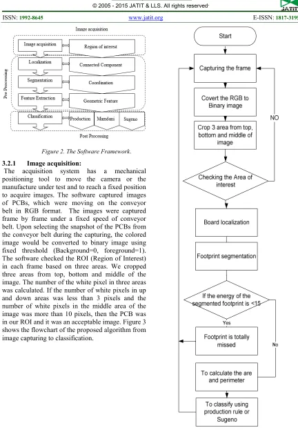
[image:4.612.87.519.56.679.2]
13 Figure 2. The Software Framework.
3.2.1 Image acquisition:
[image:4.612.344.496.80.670.2]The acquisition system has a mechanical positioning tool to move the camera or the manufacture under test and to reach a fixed position to acquire images. The software captured images of PCBs, which were moving on the conveyor belt in RGB format. The images were captured frame by frame under a fixed speed of conveyor belt. Upon selecting the snapshot of the PCBs from the conveyor belt during the capturing, the colored image would be converted to binary image using fixed threshold (Background=0, foreground=1). The software checked the ROI (Region of Interest) in each frame based on three areas. We cropped three areas from top, bottom and middle of the image. The number of the white pixel in three areas was calculated. If the number of white pixels in up and down areas was less than 3 pixels and the number of white pixels in the middle area of the image was more than 10 pixels, then the PCB was in our ROI and it was an acceptable image. Figure 3 shows the flowchart of the proposed algorithm from image capturing to classification.
14
3.2.2 Board localization:
The board localization was the first step in the preprocessing stage. This preprocessing step must include a way to delete the deviations between the acquired image and the ROI [15]. In our experiment, we used connected-component labeling operation for cropping the board from the acquired image. The 8-connectivity pixel for the connected-component labeling operation was selected based on the assumption that shapes are normally far from each other [20]. We sorted all connected-component labels and extracted the biggest one among them as the board (PCB) from the acquired image.
3.2.3 Footprint segmentation:
The footprint size and location information in board coordinates were available from a PCB design/manufacturing database for each type of board to be inspected [21]. Based on the given size of the PCB, we cropped the bounding box of each footprint from the estimated coordinates. In this step, we had to define four parameters Xmin , Ymin (coordinates), width, and height to crop the bounding box.
In this step, the energy (the number of white pixels) of the segmented image would be checked. If the energy was more than 15 pixels, we continue the next step for checking the quality of the printing in segmented footprint. If the energy was less than 15 pixels, then the footprint was considered missing.
3.2.4 Feature extraction:
The feature extraction was a critical step in image processing. The selection of suitable features was depending on the content of the images [15]. In this step, geometric features were extracted from connected-component labeling operations on the segmented footprint. We calculated two types of important geometric features namely, Area and Perimeter for each object in the image. Let V denote a (M × N) matrix with the image of a connected-component labeling operation and let Vij denote the ij th entry of V.
Then we have:
The Area A is defined as follows:
(1)
The Perimeter P is defined as follows:
(2)
3.2.5 Classification:
The last step of the proposed method was image classification. A set of the k n o wn features were calculated to classify the segmented footprint. Geometrical features such as the area and perimeter features were selected in this study for footprint classification. The quality of the printing in segmented footprints was measured in percentages and they were classified into four classes (25%, 50% 75%, 100%). The production rules, Ma md ani and Sugeno models wer e used to classify t h e s e g m e n t e d footprints. These models dealt with t h e classification of five types of PCB component footprints (Variable Resistor, IC, Capacitor, LED, and Transistor). In this step, the complete footprints (75% or 100%) were accepted and incomplete footprints (25% or 50%) were rejected.
(1)
Classification using production rule:The Production rule was experimented as one of the three classifiers in this study. A production rule system was simple and efficient. It was useful for solving classification problems when the number of classes was constant. The structure of production rule is illustrated below:
IF (value1< perimeter< value2) OR (value3< perimeter< value4) OR (value5< perimeter< value6) AND (value7 < area < value8) THEN Output is “completed footprints”
IF (value1< perimeter< value2) AND (value3 < area < value4) THEN Output is “uncompleted footprints”
(2)
Classification using fuzzy techniques:Fuzzy systems solved many machine vision problems [22]. Two fuzzy systems namely, Sugeno and Mamdani models were applied separately on feature vectors based on two geometric features. Sugeno and Mamdani fuzzy system had two inputs (A (Area) and P (Perimeter)) and just one output (O (output)).
4. RESULTSANDDISCUSSIONS:
15 and classification steps were experimented on complete and incomplete footprints on the PCB. Data samples from PCBs were collected in real time using the proposed hardware framework in the methodology section. These data samples were processed using image acquisition, localization, segmentation, feature extraction, and classification steps. In the classification step, the production rule, Mamdani and Sugeno methods were compared and discussed. The performance of each step in the software framework was evaluated.
4.1 Image Acquisition step
[image:6.612.92.299.324.479.2]The software checked the ROI in each frame based on three areas. We considered three areas from top, bottom and middle of the image. The number of the white pixel in three areas was calculated. Figure 4 shows the result of the captured image after using a fixed threshold. The performance of this methodology is depicted in Table 1.
Figure 4. The Result Of Image Acquisition
4.2 Board localization step:
In this step, we used the connected-component labeling operation to sort all connected-component labels and the biggest one among them was extracted. One of the localized boards is shown in Figure 5. The performance of the board localization step is also shown in Table 1.
Figure 5. The Localized Board
4.3 Footprint segmentation step:
In this step, we cropped the bounding box of each footprint based on its coordinates as described in methodology section. Figure 6 shows the bonding boxes of the footprints such as Capacitor, Variable Resistor, IC, LED, and Transistor on the PCB. Again, Table 1 is used to show the performance of segmentation step.
Figure 6. The Segmented Footprint
Table1. The Result Of Image Acquisition, Board Localization, Image Segmentation Steps.
4.4 Image Classification step:
The proposed AVIS used Production rule, Sugeno and Mamdani models to classify the footprints into classes.
In this study, we used 207 images to evaluate the performance of each classification models in the proposed AVIS. We considered five types of footprints and these footprints had a variety of different sizes and shapes. The accuracy value was equal to the percentage of footprints when the proposed system correctly classified the footprint in segmented images. We calculated the performance of the methods on each class of footprint according to the equation (3). The number of correct classifications is depicted in Table 2.
Table2. The Result Of Classification
Classification model
Production
rule Sugeno Mamdani
Correct
classification 95.2%
95.9
% 96.2%
Steps Number of
images
Number
of
Correct
Images
Perform
ance
Image acquisition 211 207 98%
Board localization 207 207 100%
footprint segmentation
2277 footprints
2214
[image:6.612.98.289.589.694.2]
16 In previous research [23] an automated visual inspection on printed circuit board was implemented in offline environment. Template matching was used for missing footprint detection. Table 3 shows the results of the current study in comparisons with previous work. The performance of template matching is better than production rule, Mamdani, and Sugeno, but the template matching could not classify the footprints in detail (25%, 50%, 75%, 100%). It could only classify the footprints in two classes: complete and incomplete footprints. Mamdani model is the best model to classify the footprints in detail in this study. On the other hand, the processing time of template matching is more than the other classification models. Processing time is very important issue in real time AVIS. The production rule had the shortest processing time per PCB in the proposed AVIS.
Table3. The Comparison Table
Method Environment Processing
time(s) performance
Classification in
details
Template
matching Off line 0.35 98.2% ×
Productio
n rule Real time 0.10 95.2% √
Sugeno Real time 0.20 95.9% √
Mamdani Real time 0.20 96.2% √
Therefore, performance of the proposed method is analyzed based on counting of correct (correctly classified components) and not-correct (wrongly classified components) detection on PCB. Correspondingly, number of correct and non-correct are divided by the total number of components in the performance measurement. The results of each module are discussed and presented based on the computer software evaluation standard reported in [24].
5. CONCLUSION:
The automated visual inspection system using image processing was discussed. The camera, light source and conveyor belt where the basic requirement of our real-time imaging system that were calibrated in real environment. The PCBs were moving from left to right on the conveyor belt under the camera lens. The light sources illuminated the surface of the PCBs on the
conveyor belt for capturing acceptable image. The experiment results showed that the proposed AVIS was effective to perform acquisition, segmentation and classification of the footprints. The features were extracted based on Perimeter and Area in the production rule, Mamdani and Sugeno models at the post processing stage.
The proposed AVIS consisted of three primary steps: image acquisition, pre-processing and post processing steps. The image acquisition step was the foundation for next steps and it was effective in capturing acceptable images. The preprocessing step w a s the base for post processing step in AVIS to support the classification operations. The position of the webcam, amount of illumination and the speed of the conveyor belt were the most important factors to obtain high-quality images.
In this study, the camera acquired the acceptable images effectively on footprints in real time. In image acquisition step, we captured good quality images. It meant that important information of footprints was not missed and the surface of the PCB was clear. Therefore, the webcam provided a cost-effective solution for use in real time inspection. Selecting of suitable lighting source was another contributing factor to reduce noises. From the obtained result in image acquisition step, the accuracy of image acquisition step was 98% (Table 1). This showed that the methodology in the image acquisition step worked successfully in AVIS. The result of board localization step showed that the methodology was capable to localize 100% of boards in this step (Table 1). The result of footprint segmentation showed that the methodology was capable to segment 97% of footprints.
17 real PCB in the experiments. The future work can be conducted to experiment the inspection process on real PCB products.
ACKNOWLEDGEMENT
This research is supported by MOSTI Science Fund no. 01-01-02-SF0694 and UKM Research
University grant no. UKM-GGPM-ICT-103-2010.
REFRENCES:
[1] Akbar, H. and A.S. Prabuwono, Webcam based system for press part industrial inspection. IJCSNS, 2008. 8(10): p. 170-177.
[2] Bin Mansoor, A., Z. Khan, and A. Khan. An
application of fuzzy morphology for
enhancement of aerial images. in Advances in Space Technologies, 2008. ICAST 2008. 2nd International Conference on. 2008. IEEE. [3] Aghamohammadi, A., et al., Enhancing an
Automated Inspection System on Printed Circuit
Boards Using Affine-SIFT and TRIZ
Techniques, in Advances in Visual Informatics. 2013, Springer. p. 128-137.
[4] Navarro, P., et al., A sensor system for detection of hull surface defects. Sensors, 2010. 10(8): p. 7067-7081.
[5] Haider, S., S.P. Anton, and N.H.S.A. Siti, Metal Parts Visual Inspection Based on Production Rules. Applied Mechanics and Materials, 2012. 110: p. 4091-4095.
[6] Aghamohammadi, A.H., et al. Solar cell panel
crack detection using particle swarm
optimization algorithm. in Pattern Analysis and
Intelligent Robotics (ICPAIR), 2011
International Conference on. 2011. IEEE. [7] Golkar, E., A.S. Prabuwono, and A. Patel,
Real-Time Curvature Defect Detection on Outer
Surfaces Using Best-Fit Polynomial
Interpolation. Sensors, 2012. 12(11): p. 14774-14791.
[8] http://www.techterms.com/definition/pcb. [9] Ang, M.C., et al. PCB assembly optimisation
using the Bees Algorithm enhanced with TRIZ operators. in IECON 2010-36th Annual Conference on IEEE Industrial Electronics Society. 2010. IEEE.
[10]Ang, M.C., et al., Simulations of PCB assembly optimisation based on the Bees Algorithm with TRIZ-inspired operators, in Advances in visual informatics. 2013, Springer. p. 335-346.
[11] Mogharrebi, M., et al., Missing Component Detection on PCB Using Neural Networks, in Advances in Electrical Engineering and Electrical Machines. 2011, Springer. p. 387-394.
[12] Hashim, H.S., S. Abdullah, and A. Prabuwono. Automated visual inspection for metal parts based on morphology and fuzzy rules. in
Computer Applications and Industrial
Electronics (ICCAIE), 2010 International Conference on. 2010. IEEE.
[13]Ko, K.W. and H.S. Cho, Solder joints inspection using a neural network and fuzzy rule-based classification method. Electronics Packaging Manufacturing, IEEE Transactions on, 2000. 23(2): p. 93-103.
[14] Giaquinto, A., et al., A neurofuzzy method for the evaluation of soldering global quality index. Industrial Informatics, IEEE Transactions on, 2009. 5(1): p. 56-66.
[15] Acciani, G., G. Brunetti, and G. Fornarelli, Application of neural networks in optical inspection and classification of solder joints in
surface mount technology. Industrial
Informatics, IEEE Transactions on, 2006. 2(3): p. 200-209.
[16] Prabuwono, A.S., et al. Development of intelligent visual inspection system (IVIS) for bottling machine. in TENCON 2006. 2006 IEEE Region 10 Conference. 2006. IEEE.
[17] Lin, S.-C. and C.-H. Su. A visual inspection system for surface mounted devices on printed circuit board. in Cybernetics and Intelligent Systems, 2006 IEEE Conference on. 2006. IEEE.
[18] PIRAHANSIAH, F., et al., PEAK SIGNAL-TO-NOISE RATIO BASED ON THRESHOLD METHOD FOR IMAGE SEGMENTATION. Journal of Theoretical & Applied Information Technology, 2013. 57(2).
[19] PirahanSiah, F., S.N.H.S. Abdullah, and S. Sahran, Adaptive Image Thresholding Based on the Peak Signal-to-noise Ratio. 2014.
[20] Matsushima, M., et al., Visual inspection of soldering joints by neural network with multi-angle view and principal component analysis, in Service Robotics and Mechatronics. 2010, Springer. p. 329-334.
[21] Wu, H., et al. A real-time machine vision system for solder paste inspection. in Advanced Intelligent Mechatronics, 2008. AIM 2008. IEEE/ASME International Conference on. 2008. IEEE.
18 [23] Mogharrebi, M., et al., Footprint detection on
printed circuit boards using normalized cross correlation. Visual informatic international seminar 2012., 2012.
[24] Sommerville, I., Software Engineering (9th Edition) 9th Edition, 2011.