~DmDD~D
COMPUTER LAB
COMPUTER LAB WORKBOOK
JOHN
L.
HUGHES
DESIGN ENGINEER
TABLE OF CONTENTS
PREFACE ... V INTRODUCTION ... VII OPERATING INSTRUCTIONS ... XI
CHAPTER 1 The Binary Concept ... 1
Experiment 1.1: 2-lnput NAND Gate ... ... 6
Experiment 1.2: 3-lnput NAND Gate ... 6
Experiment 1.3: 4-lnput NAND Gate ... 9
Experiment 1.4: Inverter ... ... ... 9
Experiment 1.5: Substituting Gates ... 12
Experiment 1.6: Decimal to Binary Encoder . ... 15
Experiment 1. 7: Binary to Decimal Decoder ... 18
CHAPTER 2 Basic Logic Gates ... , ... , .. , ... , .... " .... '" . . 23
Experiment 2.1: AND/NOR Gate ... 25
Experiment 2.2: NOR Gate Application of AND/NOR Gate... ... 25
Experiment 2.3: AND/NOR Comparator ... 27
Experiment 2.4: AND/NOR Gate Used for Exclusive OR ... 27
Experiment 2.5: Non-Inverting Gate ... 28
Experiment 2.6: Equality Detector ... ... 29
Experiment 2.7: Parity Bft Generator ... 31
CHAPTER 3 Flip-Flops ... '" . . . . .. . . .. .. . ... .. .... .. ... . ... ... 33
Experiment 3.1: R·S Flip·Flop .. ... ... ... ... 34
Experiment 3.2: Clocked R-S Flip-Flop ... 36
Experiment 3.3: D Type Flip·Flop ... 37
Experiment 3.4: J·K Flip·Flop ... ... 39
Experiment 3.5: 4-Bit Shift Register... 41
CHAPTER 4 Boolean Algebra to Gating Networks ... 45
Experiment 4.1: Gating Circuit Simplification ... 59
Experiment 4.2: Equality and Relative Magnitude Detector ... ... ... ... 64
CHAPTER 5 Binary Counters ... 65
Experiment 5.1: Asynchronous Binary Up Counter .... 67
Experiment 5.2: Modified Asynchronous Binary Counter ... 67
Experiment 5.3: Synchronous Binary Up Counter .... 68
Experiment 5.4: Synchronous Binary Up/Down Counter... 70
Experiment 5.5: Synchronous Modulo 6 Binary Counter ... 73
Experiment 5.6: Asynchronous Self-Stopping Modulo 13 Binary Counter... 73
Experiment 5.7: Variable Modulus Asynchronous Binary Up Counter ... 74
CHAPTER 6 Serial Addition ... ... ... ... ... ... 79
Experiment 6.1: Serial Adder ... 83
CHAPTER 7 Parallel Addition ... 87
Experiment 7.1: Parallel Adder ... 90
Experiment 7.2: Two's Complement Subtraction ... 92
Experiment 7.3: One's Complement Subtraction ... 93
Experiment 7.4: One Step Parallel Addition ... 93
CHAPTER 8 Binary Coded Decimal Operations ... 95
Experiment 8.1: The 8421 Counter ... 95
Experiment 8.2: The Excess 3 Counter... 96
Experiment 8.3: The 2421 Counter ... 9Q Experiment 8.4: The 5421 Counter ... 96
Experiment 8.5: Serial BCD Addition ... 101
CHAPTER 9 Code Conversion and Decoding ... 105
Experiment 9.1: The 2421 to 8421 Converter ... 110
Experiment 9.2: The 5421 to 8421 Converter... .... 113
Experiment 9.3: Gray to Binary Converter.. ... ... 115
CHAPTER 10 System Considerations ... 119
Experiment 10.1: Parallel Adder Control... 122
Experiment 10.2: Synchronizers ... 123
Experiment 10.3: Maximum Frequency.. ... ... ... 126
Appendix A: Checkout Procedures ... 129
Appendix B: Karnaugh Mapping ... 135
Appendix C:
,
TTL Circuitry ... 139Appendix D: The Computer... 145
Appendix E: Glossary of Terms ... 156
Appendix F: Decimal to Binary Conversion Table ... 163
Appendix G: Powers of Two ... 165
Appendix H: Recommended Texts ... 166
Appendix I: COMPUTER LAB Hardware Specifications ... 167
Appendix J: Warranty ... 169
PREFACE
This workbook contains a complete course in digital logic. It is intended to accompany courses in binary arithmetic, Boolean algebra, digital logic or computer technology. The workbook was developed to be used with Digital Equipment Corporation's COMPUTER LAB.
Much more material is presented than could be used in any full year labora-tory course. The extra material is included to allow particular sections of a course to be emphasized with larger amounts of experimental time. Most chapters have a main theme experiment followed by a number of sub·experi· ments that can be used for emphasis. The information presented in the sub-experiments is not needed to understand later sections of the book and these sections can be considered supplementary.
The workbook material is prepared on five levels of instruction. The first level is an introduction to the binary concept. The student is shown how two states can be used to both perform logic functions and count. Basic logic functions on the COMPUTER LAB are studied, and the correlation between the binary and decimal systems is demonstrated.
The second level provides a close look at the logic elements available on the COMPUTER LAB. The student uses the simpler logic gates to construct some of the more complex devices. This way, he gains a much greater understand-ing of these complex mechanisms than would be possible by studyunderstand-ing a com-plete unit.
At the third level, the student studies Boolean algebra, logic truth tables and how the transition from a logic requirement tel a gating network is accom-plished. This level uses the complete complex logic elements studied in detail in the previous level.
The fourth level deals with digital subsystems, beginning with an explanation of the mathematical process of binary addition. This level also discusses methods of complementary binary subtraction, binary coded decimal count-ing, and code conversion.
The final level of learning brings together the knowledge from previous levels by discussing digital systems.
My thanks go to all the people who have assisted in the writing, preparation and revision of this book. In particular, I would like to acknowledge the help given by the following individuals from Digital Equipment Corporation: Mr. G. Del Rossi, Mr. D. Doyle, Mr. R. Nelson, Mr. J. Richardson; and also, Mr.
J. Knott, Thistletown Collegiate Institute; Mr. J. Miller, Ryerson Polytechnical Institute; Dr. K. Smith, University of Toronto.
GENERAL,FEATURES
With the COMPUTER LAB, DIGITAL offers a complete teaching package. The unit and workbook are supplemented by the COMPUTER LAB Teacher's Guide which includes detailed course plans, complete answers for all the questions in the workbook, additional pictorial wiring diagrams, suggested test ques-tions and supplementary instructional text.
• Teaches modern computer logic.
• Comprehensive Workbook includes basic text material and ten detailed experiments.
• Provides up to 200 hours of laboratory study.
• The ten basic chapters are divided into more than 30 experiments. • Teacher's Guide with answers, additional text, extra problems, and course
plans.
INTRODUOTION
Computers and computer technology are assuming roles of increasing impor· tance in today's technically oriented civilization. It is becoming more and more necessary that secondary schools give students a basic knowledge of computer fundamentals. For all students, instruction in basic computer con-cepts helps present and reinforce the important "New Math" principles of binary arithmetic and Boolean algebra. For the technical student, a knowledge of computer fundamentals can open a rewarding career in the computer industry.
The explosive growth in the use and application of computers has created a tremendous, mostly unfilled, demand for trained people. By 1970, according to a recent survey, there will be between 100,000 and 150,000 computers in use. This means that in the next few years, the computer industry will require more than 150,000 new programmers, over 200,000 new systems analysts, more than 90,000 new managers and supervisors, plus about 20,000 people to replace those lost through attrition.
As the computer gradually eliminates jobs in some areas, others are created requiring new skills and placing new demands on our educational system. Educators in ever growing numbers agree that all students should receive at least a basic introduction to the fundamentals of computer technology. All students will benefit from exposure to fundamental computer concepts, for the mathematical principles that form an important part of computer tech-nology are also important in general mathematics programs.
Education in basic computer concepts should begin in secondary schools and be complemented by specialized training in vocational schools and advanced college study. Many educators have already accepted this responsibility and instituted computer technology courses. Texts, curricula and other materials prepared by the United States Office of Education, the National Science Teacher Association, The Association for Computing Machines and others, stress that initial education in computer science should emphasize the basic concepts and principles that apply to all digital computers. Chief among these are:
1) Binary arithmetic-the "machine language" of most present day computers
2) Principles of digital logic-the electronic "switches" that allow computers to operate and make decisions
3) Two·state memory devices
4) Boolean algebra-the rules for logic manipulation
In teaching computer technology and its associated mathematical concepts, the student benefits most if he learns the basic principles first, if he becomes thoroughly familiar with binary arithmetic, Boolean algebra and digital logic. From this foundation, all other computer·related education builds naturally and easily, allowing the student to continue his education with the least effort and best preparation into any of the many careers created by the expanding computer technology, from computer mathematics to programming to electronic engineering.
THE COMPUTER LAB
Digital Equipment Corporation has had extensive experience in computer education, with over half of its 3000 installed PDP computers in educational
institutions. DIGITAL found a need for a training device to teach basic com-puter concepts and so developed the COMPUTER LAB, a classroom laboratory for teaching digital logic and computer fundamentals.
The COMPUTER LAS- is a complete educational package for teaching the fundamental concepts underlying the theory and operation of all digital com-puters. In clear experiment-lessons, the student is given step-by-step instruc-tions in digital logic principles. After mastering the basic material presented in the COMPUTER LAB course, the student can progress easily through advanced study into many of the computer-related disciplines. The digital logic fundamentals presented in the course constitute the basic knowledge a student needs to build a career as a computer technician or electronics engineer. A programmer, if he is to use a computer to its fullest potential, must also be thoroughly familiar with a computer's basic operating principles. An important part of computer technology is the "New Math". Once, the binary number system and Boolean algebra were interesting sideroads of mathematics. Now the computer has given them new importance, for the computer understands only the binary language and follows the laws of Boolean algebra. Everyone in school today is exposed to these two vital elements of the New Math. The COMPUTER LAB not only operates with binary numbers according to Boolean algebraic laws but graphically demonstrates these two important concepts. For every student, whether he intends to find a career within the computer industry or not, the New Math is important and the COMPUTER LAB makes it easier to understand. Students going on to college will need to use computer concepts in mathematics, science and engineering studies. For the technical or vocational student,
.a
knowledge of the computer can 'lead to a career in the computer industry.STEp· BY ·STEP INSTRUCTION
The COMPUTER LAB incorporates the latest advances in computer technology and the workbook gives the student step-by-step instructions. Each instruction can be followed by wiring the unit with the easily inserted and removed patch cords and by testing final designs. The course provides a basic set of ten chapters, each divided into many complete experiments. Each chapter deals with a basic 1:0mputer principle and the entire course fully illustrates the whole range of digital logic principles.
THE COMPUTER LAB COURSE
As a laboratory instrument for classroom training in digital logic, the unit can provide a course lasting a full semester, comprising over 200 hours of lab-oratory work supplemented by 50 hours or more of lecture.
The basic course is organized on five levels of instruction. The instructor can follow the course material as presented in the workbook or is free to tailor the course to emphasize specific subject matter, grade levels or rates of instruction by deleting certain sections and/or adding supplementary informa-tion in other areas.
The COMPUTER LAB is designed for classroom use in high schools, technical schools, junior colleges and universities. It can be used for logic circuit ex-perimental work in research laboratories and in industry. During laboratory work, at every level of instruction, the student has the opportunity to learn by doing. At any level, he may easily move back to a lower level to reinforce some of the more basic concepts taught earlier. As the student becomes more adept, he may connect several COMPUTER LABs together, one super-vising the other, to enlarge computational power .
•
~
JI
~JI ~JI ~Cl
1<0 KO k O 1<0
II II " "
~~~SD-b~
~~
HIGH HIGH HIGH
<>-<> 0-0 C>-O
~ ~ ~ ~
~ ~ -~ ~
HIGH HIGH HI6H
0-0 C>-O C>-O
~~~~SD-b
={F
~'
={F~
I~~'
~J
IK 0 GNO M M _ II
e>-o <>-<>
COMPUTER LAB
IWI TeH OUTPUTS e>-oo-oo-o 0-00-0 0-0 o-oe>-o
LAMP IIiI'UTS o-oe>-oo-oo-oo-oo-oo-o<>-<>
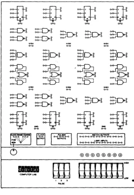
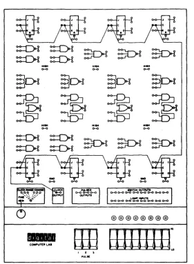
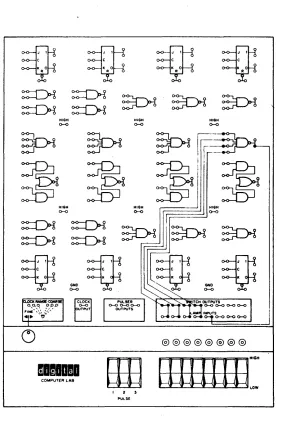
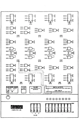
[image:12.384.50.323.79.473.2]COMPUTER LAB OPERATING INSTRUCTIONS
LOGIC LEVELS
There are two logic levels used on the COMPUTER LAB; HIGH (HI) and LOW (La). Several terminals are provided on the patchpanel to give a HIGH logic level.
II ROCKER SWITCHES
Rocker switches can be used to provide either a HI or a La logic level. If the upper side of the rocker switch is depressed, the two corresponding switch output terminals (directly in front of the switch) are taken to a H I level. If the lower side of a rocker switch is depressed, the two corresponding output terminalsare taken to a La level.
III PULSER SWITCHES
The outputs of the pulser switches are normally LO. When a pulser is de-pressed, the corresponding two output terminals go to a HI level. When t.he pulser is released its output terminals return to the La condition. Internal circuits connected to the pulsers make sure that when a pulser is depressed or released, electrical noise generated in the switch is not transmitted to the pulser output. This special circuitry makes the pulsers useful in applications requiring noise-free transitions from one level to another. Rocker switches do not have this feature.
IV PULSES
Pulses are voltages which go from one logic level to another for a short time and then return to the original level. All pulses have a width which is defined as the length of time for which the pulse voltage is at the second or transient level. HI PU LSES a re ones wh ich ,go from La to H I for a short time, then back to La. LO PU LSES are ones which go from H I to La for a short time, then back to HI. Pulses can occur one at a time or in a pulse train. Pulse trains have pulses which occur at a certain repetition rate, normally measured in pulses per second. (See Figure 2.)
V CLOCK
The clock provides a continuous train of HI pulses. Clock pulses are 50
50
\/oLTAGE
LO~----~--~---~----~---~--~--Figure 2
F· FREQUENCY W' PULSE WIOTH
High Pulse Train
CLOCK RANGE COARSE
qq pPIJ
' " \ J I /
FINE '~\\ J~ / ~
...
Figure 3 Clock Range Set Slow
VI LAMP INDICATORS
TIME (SEC)
The operation of experiments constructed on the COMPUTER LAB patchpanel is monitored by the lamp indicators. A lamp will be ON if its corresponding input is at a HI logic level. A lamp will be OFF if the corresponding input is at a LO logic level. If no connection is provided to a lamp input, the lamp will be OFF. Lamps will respond to sustained logic levels and pulses of sufficient duration to activate the lamp filament. '
VII UNUSED INPUTS
Unused inputs to gates and flip-flops should be connected to the HI terminals provided on the patchpanel. It is especially important to connect flip-flop Re· set inputs to a HI terminal when they are used in counters, shift registers, etc., with no Reset provision. Unless this is done, flip-flops will not operate properly.
VIII USING TWO OR MORE COMPUTER LABS TOGETHER
Often there are applications where it is necessary to use two or more COM-PUTER LABS to construct large logic circuits. To use COMCOM-PUTER LABS in this way, connect wires from the GND (ground) terminals on the patchboard of one COMPUTER LAB to GND terminals on the other units. When construct-ing circuits of this nature, it is best to try to build major circuit sections on each COMPUTER LAB. This sectional construction will keep the number of logic circuit interconnections between COMPUTER LABS to a minimum. Each COMPUTER LAB used in a large circuit must be plugged in and turned on.
IX WIRING ON COMPUTER LAB
@@@@@@@@
--
COMf'UT£R L ....EW
LlllllIE~
, 2 5
[image:15.384.36.317.86.469.2]PULst:
CHAPTER 1
THE BINARY CONCEPT
INTRODUCTION
There are
a
large number of devices with only two states or possible condi-tions. For example, a light switch has only two states: it can be on or off. Similarly, a doorbell button can be either pressed or released, causing a bell to be on or off. The point of a ball pOint pen can be either extended or retracted. These two-state devices can be classed into two groups. Group 1 has memory, Group 2 does not have memory. for example, a light switch has memory; it remembers the last state it was put into. If it is turned on, it remains on until it is turned off. The ball point pen also has memory; if the point is extended it remains extended until the button at the end of the pen is pushed to retract it. Once the point is retracted, it remains retracted until it receives a command to extend. The door bell push-button is a device without memory; the bell will ring only as long as the button is depressed. Once the button is released it does not remember that it has been depressed and the bell stops ringing.Decisions are often based on a number of YES or NO type conditions, two-state conditions. For example, if a driver sees a red light OR a stop sign OR an obstacle in the path of travel of his car, he stops. Symbolically the stop decision could be represented as in Figure 1.1. Each one of the conditions which would make the driver stop are either present or not present. They are two-state conditions: the red stop light can be on or off; the stop sign can be present or not present; the obstacle can be present or not present. If any one or more of these conditions is present, the driver will stop. All possible combinations o"f conditions which can occur can be represented in a table. Figure 1.2 is a table showing all the possible conditions that can occur be-tween the stop light, stop sign and the obstacle. This type of table is known as a truth table. The number of possible conditions in a two-state truth table is equal to 2N where N is the number of two-state variables considered.
STOPLIGHT
=i:J-STOPSIGN OR STOP OBSTACLEFigure 1:1 Stop Decision
"
CONDITIONS RESPONSE
Stop Sign Obstacle
Stop Light (Stop)
No No
No Yes
Yes No
Yes Yes
No No
No Yes
Yes No
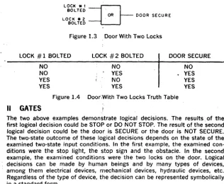
Mechanical situations can also: be represented in
a·
symbolic form. If, for in-stance, a door has two locks, the door would be secure if one lock or the other lock is bolted. Figure 1.3 shows how this condition can be represented sym-bolica"y. Again, a" possible conditions that can exist with the locks can be represented in a truth table, as shown in Figure 1.4.LOCK *1 BOLTED
=8-.. OR DOOR SECURE LOCK.2 ..
BOLTED
Figure 1.3 Door With Two Locks
LOCK
#
1 BOLTED LOCK#
2 BOLTED DOOR SECURENO NO YES YES
II
GATES
NO YES NO YES
Figure 1.4 Door;With Two Locks Truth Table NO YES YES YES
The two above examples demonstrate logical decisions. The results. of the first logical decision could be STOP or DO NOT STOP. The result of the second logical decision could be the door is SECURE or the door is NOT SECURE. The two·state outcome of these logical decisions depends on the state of the examined two-state input conditions. In the first example, the examined con-ditions were the stop light, the stop sign and the obstacle. In the second' example, the examined conditions were the two locks on the door. Logical decisions can be made by human beings and by many types of devices, among them electrical devices, mechanical devices, hydraulic devices; etc. Regardless of the type of device, the decision can be represented symbolica"y in a standard form.
OR Gate
The OR logical decision has been demonstrated in both the above examples. The standard symbol for this logical OR decision is shown in Figure 1.5. This symbol is called an OR gate. The inputs or conditions examined by an OR gate are on the left of Figure 1.5; The result or output of an OR gate is on the right of Figure 1.5. OR gates may have two or more inputs but only one .output. Figure 1.5 shows a two-input OR gate. The OR condition is met, or the gate is enabled, if one or more of the inputs is present. In general, a gate is enabled when its input conditions are met. The driving example described earlier can be represented in a standard symbolic form as shown in figure 1.6 by a 3-input OR gate. This gate will operate 'a~ described in the truth table in Figure 1.2.
I "PUTS {
~
} OUTPUT [image:18.383.28.345.81.341.2]STOPLIGHT
=D-STOPSIGN STOP
OBSTACLE
Figure 1.6 OR Driving Decision
AND Gate
Another type of decision involves the AND function. For example, if a driver were at an intersection when the light turned green AND the path of travel were clear, the driver would go. Both input conditions must be present before the driver can go. Figure 1.7 shows a symbolic representation of this AND decision. Figure 1.8 is a truth table showing all the possible input conditions and the resultant output conditions. (Note: there are 22 possible combina-tions of the two two-state variables.) The AND gate can have two or more in-puts, all of which must be present for the gate to be enabled.
Inverter
PATH CLEAR
=D-GO GREEN LIGHTFigure 1.7 AND Driving Decision
Light Green Path Clear Go
No No Yes Yes No Yes No Yes No No No Yes
Figure 1.8 AND Driving Decision Truth Table
There are applications where it is convenient to take information and change it into its opposite state. A device to perform this function is known as an INVERTER. The symbols for an inverter are shown in Figure 1.9. If an inverter receives YES information at its input on the left, it would give NO information at its output on the right. If it received NO information at its input, it would give YES information at its output. Figure 1.10 is a set of truth tables which show the operation of the inverter. Figure 1.10(a) shows how the inverter can be used to invert YES or NO information.
INPUT
I
OUTPUTNO YES 1.10(a)
NO
---{>---
YESFigure 1.9 Inverter
INPUT 1
o
OUTPUTo
1 1.10(b) INPUT AA
OUTPUT A A 1.10(c)Figure 1.10(b) shows how the inverter can be used to invert 1 or 0 informa· tion, a 1 representing a YES, a 0 representing a NO. Figure 1.1 O(c)shows a method of representing condition "A" and the inversion of that condition "not A." Not A, or the invers19n of A, is representee!. by
A.
If A is at the input of the inverter, its opposite, A, is at the output. If A is at the input of an in· verter, its opposite, A, is at the output.Summary
In an OR gate, the output is 1, or the gate is enabled, whenever one or more of the inputs are 1. The output of an OR gate is 1 if anyone or more of the following conditions are met: input A is 1, OR input B is 1, OR input C is
1, etc.
In an AND gate, the output is 1, or the gate is enabled when, and only when, the inputs are 1, regardless of the number of inputs. The output of an AND gate is 1 only when input A is 1, AND input B is 1, AND input C is 1, etc. In an Inverter, the output is always the opposite, or inverse, of the input. An output is 1 when its input is O. An Inverter output is 0 when its input is 1.
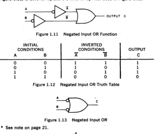
Negated Input OR Gate
The inverter can be used with the AND and OR gates to extend their capabil· ities. If both inputs to an OR gate are fed through inverters, as in Figure 1.11, the OR gate functions in an opposite or complementary manner. With in· verted inputs, the OR function will be present when one input, or the other, or both, are not present. In other words, the negated input OR gate will be enabled when one or both inputs are not present. Figure 1.12 shows the truth table for a 2·input negated input OR gate. A "1" represents a"present"or YES condition. A "0" represents a"not present"or NO condition. In standard sym-bology, a small circle on the input line of an OR gate symbol, as shown in Figure 1.13, is used to replace the inverter symbol used in Figure 1.11.
A
~OUTPUTC
Figure 1.11 Negated Input OR Function
INITIAL CONDITIONS
INVERTED CONDITIONS
A
B
A
8
o
o
1 1o
1o
1 1 1o
o
1o
1o
Figure 1.12 Negated Input OR Truth TableFigure 1.13 Negated Input OR
=00 See note on page 21.
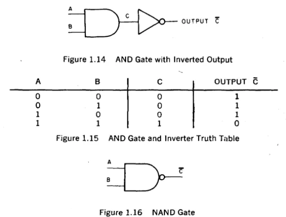
[image:20.379.28.334.291.554.2]NAND Gate
Similarly, an AND gate, with an inverter at its output, can be used to perform an opposite or complementary function, as shown in Figure 1.14. The truth table for this function in Figure 1.15 shows that the output from the inverted AND will not be present when both inputs are present. The inverted AND function is enabled when both inputs are present. This type of gate is repre-sented in Figure 1.16 with a small circle attached to the output of the AND gate to replace the inverter symbol. Since the gate is performing a "not" AND function when enabled, it is called a NAN 0 gate.
~OUTPUTC
Figure 1.14 AND Gate with Inverted Output
A B C OUTPUT
C
0 0 0 1
0 1 0 1
1 0 0 1
1 1 1 0
Figure 1.15 AND Gate and Inverter Truth Table
Figure 1.16 NAND Gate
Equality of NAND and Negated Input OR Gates
If the truth tables for the negated input OR gate and the NAND gate are com-pared, as in Figure 1.17, it is readily evident that they are identical. For cor-responding input conditions, the output conditions are equal for the NAND and negated input OR gates.
A B OUTPUT A B OUTPUT
0 0 1 0 0 1
0 1 1 0 1 1
1 0 1 1 0 1
1 1 0 1 1 0
Figure 1.17(a) Negated Input Figure 1.17(b) NAND Gate OR Gate Truth Table Truth Table
[image:21.383.45.340.120.344.2]III COMPUTER LAB LOGIC FUNCTIONS
The COMPUTER LAB uses electronic logic functions which recognize two voltage levels, HI and LO. It is advisable at this time to review the COMPUTER LAB specifications for rocker switches and lamp indicators given in the intro-duction. The COMPUTER LAB uses inverting logic for a number of reasons. Chief among these is the versatility and ease of use_ Also, all modern com-puters use inverting logic elements.
EXPERIMENT 1.1: 2-INPUT NAND GATE
Figure 1.18 shows a NAND gate with the inputs connected to rocker switches which can provide either a HI or a LO signal on either gate input. The output is connected to a lamp indicator. The same circuit is shown pictorially in Figure 1.19. Construct this circuit on the COMPUTER LAB. The rocker switch outputs are also connected to indicator lamps to give a visual indication of the input condition.
ROCKER SWITCHES
HI
LO - - - 0
H I - - o
LO - - - 0
Figure 1.18 2-lnput NAND Gate Test Circuit
TO LAMP INDICATOR
Figure 1.20 is a truth table showing the operation of a 2-input NAND gate. Test the NAND gate by checking each condition of the truth table and filling in the final column to indicate whether the lamp was on or off, with H I repre-senting the lamp on, and LO reprerepre-senting the lamp off. Compare the truth table you have made to the one in Figure 1.15.
SWITCHES LAMP INDICATOR
A
B
LO LO
LO HI
HI LO HI
HI HI
Figure 1.20 NAND Gate Truth Table
EXPERIMENT 1.2: 3-INPUT NAND GATE
~
JI
~J\ ~J\ ~JI
" , 0 K O K O teO
A It R R
~~~~~
HIGH HIGH HIGH0-<> 0-0 0-<>
HIQH 0-<>
HIQH 0-<>
HltH
0-0
~
JI
~JI
~JI
~J'
K 0 K K •
OND . OND
0-0 0-<>
LAMP INPUTS 0-0 0-0 0-0 0-0 c>-o
@@@@@@@@
mamaama
ErE
BlIlllE=
COMPUTER LAB
I Z ,
PULSE
Figure 1.19 2-lnput NAND Gate Test
[image:23.378.47.341.69.449.2]~
KOJ'
~c' ~J'
KO < 0=Q!c'
K OR R R R
~ ~ ~ ~
~~~~
HIGH HIGH HIGH o-<l o-<l o-<l(5.
@@@@@@@@
mamlDla
COMPUTER LAB
, 2 3
PU~Sf
[image:24.380.43.319.67.450.2]tf',
A B C OUTPUT
LO LO LO HI'
LO LO HI HI
LO HI LO
LO HI HI
HI LO LO
HI LO HI
HI HI LO
HI HI HI
Figure 1.22 3-input NAND Gate Truth Table
EXPERIMENT 1.3: 4·INPUT NAND GATE
Test the operation of the 4-input NAND gate on the COMPUTER LAB by connecting the circuit shown in Figure 1.23. Complete the final column in the truth table in Figure 1.24, with a HI indicating the lamp on, and a LO iridi-cating the lamp off.
A B C 0 OUTPUT
LO LO LO LO HI
LO LO LO HI HI
LO LO HI LO HI
LO LO HI HI
LO HI LO LO
LO HI LO HI
LO HI HI LO
LO HI HI HI
HI LO LO LO
HI LO LO HI
HI LO HI LO
HI LO HI HI
HI HI LO LO
HI HI LO HI
HI HI HI LO
HI HI HI HI
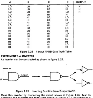
Figure 1.24 4-lnput NAND Gate Truth Table
EXPERIMENT 1.4: INVERTER
An inverter can be constructed as shown in figure 1.25.
OUTPUT - - - - . INPUT
~
I
Figure 1.25 Inverting Function from 2-lnput NAND
[image:25.381.24.341.194.524.2],,,(0
~
Jt
~Jt ~Jt ~Jt
k O k O k O k O
" " " II
~~~~~
HIGH HIGH HI8M
0-0 0-0 0-0
@@@@@@@@
-
..
COMPUTER LAB
I Z ~
PULSE
[image:26.378.50.333.42.472.2]~
Jt
K O~ct ~~t ~ct
K O K O K OR R R R
~~~~~
~~~6
HIGH HIGH HIGH
~ 0--0 ~
~ ~ ~ ~
~~~~
HIGH HIGH Hl(iH0--0 ~
~~~~~
~
-K 0 K : J( K
GND ' GND
0--0 ~
SWITCH OUTPUTS 0--0 CH) 0--0 0--0 0--0 CH) 0--0
LAMP INPUTS
0-0 0--0 0--0 0--0 0-0 0--0
@@@@@@@@
malilla
COMPUTER LAB
t 2 5 PULSE
[image:27.380.45.322.40.466.2]constant HI to one input of a 2-input NAND gate, the gate becomes, in effect, a I-input NAND gate. The condition of the one remaining input now controls the gate output. If the remaining input is HI, the gate output will be LO; if that input is LO, the output will be HI. The gate is now functioning as an in-verter. The standard inverter symbols are shown on the right of Figure 1.25.
INPUT LO HI
OUTPUT
Figure 1.27 Inverter Truth Table
EXPERIMENT 1.5: MULTIPLE INPUT GATE USAGE
There are logic systems and subsystems to be constructed on the COM-PUTER LAB which will require more NAND gates with a specific number of inputs than are available on the patch panel. In cases such as this, gates with a greater number of inputs can be substituted for gates with fewer inputs. For instance, a 4-input gate can be substituted for a 3-input gate by connecting the unused input to a HI level and using the other 3 inputs as a normal 3-input NAND gate. Connect the circuit shown pictorially in Figure 1.28 and complete the truth table for this 4·input NAND gate used to substitute for a 3-input NAND gate, as shown in Figure 1.29.
[image:28.378.26.344.236.532.2]A LO LO LO LO
HI
HI
HI HI QUESTIONS B LO LO Hl HI LO LOHI
HI
C LO HI LO HI LO HI LO HI OUTPUTHI
HIFigure 1.29 Truth Table for 4-lnput NAND Gate Used as 3-lnput NAND Gate
1. Make a truth table similar to the one you have completed in Figure 1.20 for a two-input NAND gate when used as an inverter. Which conditions on the initial truth table cannot occur? Why?
2. When a 4-input NAND gate has one of its inputs connected to HI, what conditions cannot occur in the truth table in Figure 1.24?
3. Show how a 3-input NAND gate can be used as an inverter.
4. Show two techniques for using a 3-input NAND gate as a 2-input NAND gate.
5. Explain why a NAND gate can be used to perform the negated input OR function.
IV
BINARY NUMBERS
apart-~~~~~
~~~
HIGH HIGH HIGH
0-0 0-0
~ ~ ~
r.----
K>-'rI--/~ ~ ~Il~
HIGH H I G H .II
HIGH~~~ ~r~~~
~
JI
~cl III~JI
~JI
. 0 • 0 0 0 0
GND GND
0-0 0-0
mlliDma
COMPUTER LAB
I 2 ,
PUl..SE
Figure 1.28 4-lnput NAND Gate Used as a 3-lnput NAND Gate
[image:29.381.34.323.60.441.2]ment with the first digit of the number indicating the floor of that apartment and the second digit indicating the number of the apartment on that particu-lar floor. The logical sequence of numbers would be 00, 01, 02, 03, 04, 05, 06, 07, 10, 11, 12, 13, 14, 15, 16, 17, 20, 21, . . . etc. This counting se-quence has used only 8 unique states or digits. The digits used are 0, 1, 2, 3, 4, 5, 6, 7. The number system is called the octal number system, because it has a base of 8 distinct states.
BINARY DECIMAL
26 25 24 23 22 21 20 102 10 1 100
0 0 0 0 0 0 0 0 0 0
0 0 0 0 0 0 1 0 0 1
0 0 0 0 0 1 0 0 0 2
0 0 0 0 0 1 1 .0 0 3
0 0 0 0 1 0 0 0 0 4
0 0 0 0 1 0 1 0 0 5
0 0 0 0 1 1 0 0 0 6
0 0 0 0 1 1 1 0 0 7
0 0 0 1 0 0 0 0 0 8
0 0 0 1 0 0 1 0 0 9
0 0 0 1 0 1 0 0 1 0
0 0 0 1 0 1 1 0 1 1
0 0 0 1 1 0 0 0 1 2
0 0 0 1 1 0 1 0 1 3
0 0 0 1 1 1 0 0 1 4
0 0 0 1 1 1 1 0 1 5
0 0 1 0 0 0 0 0 1 6
0 0 1 0 0 0 1 0 1 7
0 0 1 0 0 1 0 0 1 8
1 1 0 0 1 0 0 1 0 0
1 1 0 0 1 0 1 1 0 1
1 1 0 0 1 1 0 1 0 2
Figure 1.30 Binary Counting Sequence
Similarly, if there are only two unique states to work with, a counting system can be evolved: this is the binary or two-state counting sequence. Figure 1.30 shows the binary count sequence and decimal numbers of corresponding value_ Digital computers are composed of two-state logic elements which can use the brnary system. Just as the decimal system is based on powers of 10, the binary system is based on powers of 2. Each binary digit carries a weight or multiplier which is a power of 2, as shown in figure 1.30. The least sig-nificant, or right-most digit, carries a weight or multiplier of 20 or 1. The next most significant binary digit carries a weight or multiplier of 21. The next most significant binary digit carries a weight or multiplier of 22 and so on. A detimal number is weighted with the right-most column having a multiplier or weight of 100 • The next most significant column has a multiplier of 10 I or 10.
The next most significant column has a weight of 102 or 100, and so on. For instance, the decimal number 136 is equal to:
1 X 10²
+
3 X 10 1+
6 X 100•likewise the binary number 1100 is:
1 X 23
+
1 X 22+
0 X 21+
0 X 20V DECIMAL TO BINARY CONVERSION
To convert a binary number into decimal.add the decimal weights of each binary bit which is a 1. Thus the binary number 1001100 is equivalent in value to the decimal number 26
+
23+
22=
76. This binary to decimal conversion suggests a method for converting decimal numbers into binary numbers.That method is to subtract the largest power of 2 which is less than or equal to the decim.al number being converted. The second step is the same as the first and it is performed on the remainder from the first step. The process continues until the remainder of successive subtractions equals O. Example, convert 76 into binary.
-76-26
=
1212-23
=
44-22
=
0Thus 76 equals 26
+
23+
22. As was shown in Figure 1.30. the 22 is the third position from the right of a binary number; 23 is the fourth position from the right of a binary number; 26 is the seventh position from the right in a binary number. The binary equivalent of a decimal number 76 is, therefore, 1001100.QUESTIONS
6. Convert the following binary numbers into decimal:
A) 10010110 F) 100011110 B) 0110011 G) 10011001
C) 11110111 H) 10101010 D) 1000001 I) 110110110 E) 0001000 J) 011011011
7. Convert the following decimal numbers into binary:
A) 148 F) 4 X 10³
B) 277 G) 49
C) 53 H) 875
D) 256 I) 94
E) 512 J) 117
EXPERIMENT 1.6: DECIMAL TO BINARY ENCODER
To communicate with a computer. it is necessary to convert input informa-tion into the binary language which the computer understan~s. One device that does this translation is an encoder. Figure 1.31 shows an encoder for converting the decimal digits 0 to 7 into a three-bit binary number. Construct the circuit on the COMPUTER LAB according to the pictorial diagram in Figure 1.32. Recall that the NAND ated in u ates are the same in funct! ga es on the COMPUTE B can be use
TO LAMP INDICATORS
HI
LO 4 3 2
ROCKER SWITCHES
Figure 1.31 Decimal to Binary Encoder
Decimal To Binary Encoder Operating Instructions
1. Set all the rocker switches to the HI condition. Observe and record the condition of the lamps.
2. Set the"I"rocker switch to the LO condition. Observe and record the con-dition of the lamps.
3. Reset the"l"rocker switch to the H I condition. Set the"2"rocker switch to the LO condition. Observe and record the condition of the lamps. 4. Continue setting one rocker switch at a time to the LO condition and
observe and record the indication obtained on the lamps for each of the 7 rocker switches.
QUESTIONS
8. Compare the recorded indication of the lamps which you have obtained to the binary count sequence in Figure 1.30.
9. At what level (HI or LO) should a switch input be for conversion? Why? 10. At what level must all switch inputs other than the ones being converted
be? Why?
11. Explain the operation of the decimal to binary encoder by explaining the operation of each gate.
[image:32.380.43.351.61.450.2]\
22 2\ 20
@@@@@@@@
--
COMPUTER LABI I S 7 6 !I 4 3 2. \ 0
~'E
[image:33.379.27.310.59.460.2]EXPERIMENT 1.7: BINARY TO DECIMAL DECODER
When a computer has completed an operation the answer is usually given in binary form. Since most people are used to working in decimal, it is often necessary to decode the output information. One method is to use a NAND gate decoder, such as the one shown in Figure 1.33. The partial truth table in Figure 1.35 shows the operating rules for the decoder. Note that in the' table the (-) symbol is used to indicate negation.
For example, when ~ is a I, it indicates that the 2° switch is in the LO posi-tion, or that the 2° bit is a 0 in the number being decoded. To detect the number 101, a NAND gate would look for the conditions 22,
2i
and 20. When that NAND gate is enabled, it would indicate the presence of the number 101 by giving a LO output (which could turn a lamp out). Complete the truth table in Figure 1.35 to show the complete operating rules for the 3-bit binary to decimal decoder. Construct the decoder as shown in the pictorial diagram in Figure 1.34.22 21 20 22
2i
20
0 0 0 1 1 1
0 0 1 1 1 0
'0 1 0 1 0 1
0 1 1
1
1
Figure 1.35 Binary to Decimal Decoder Operating Truth Table
Binary To Decimal Decoder Operating Instructions
DECIMAL
o
1 2 3 4 5 67
1. Place all sw.itches in the LO position. Observe and record lamp outputs. 2. Place 20 switch in the HI position. Observe and record lamp outputs. 3. Return 20 switch to the LO position. Place 21 switch to the H I position.
Observe and record lamp outputs.
4. Continue testing the decoder by plaCing the switches in the positions indicated by the binary count sequence in Figure 1.30 with a HI repre-senting a 1, and LO reprerepre-senting a O.
QUESTIONS
13. Explain how the logic elements in the binary to decimal decoder operate. 14. Design and construct the circuitry necessary to decode the binary num·
ber 101 into the decimal number 5.
15. Design the circuitry to decode the binary numbers up to 1111 into decimal.
16. Why is a base 2 number system well suited for two-state devices such as those used on the COMPUTER LAB?
SUPPLEMENTARY QUESTIONS
TO LAMP INDICATORS
2'
LO HI
Figure 1.33 Binary to Decimal Decoder
[image:35.384.34.350.20.526.2]:=Q!
K OJ ,
~J
K O ,~J
K O,
:=Q!J
•,
It It It R
@@@@@@@@
1 1 5 4 3 2 1 0
COMPUTER LAB
Em
UlllllE=
1 2 3 22 2'zO
1'ULSf:
[image:36.385.40.326.67.461.2]DEVICE 1 DEVICE 2
LO LO
LO HI
HI LO
HI HI
ABCDEFGHIJKLMNOPQRSTUVWX 0 0 0 0 0 0 1 1
1 1 2 2 3 3 0 0 2 3 1 3 1 2 2 · 3 2 3 1 2 1 3 · Figure 1.36
Which of the 24 ways is easiest to follow and expand? Why?
Expand the code you have chosen to show the truth table for the complete count sequence available if four 2-state devices were used. 18. Construct a truth table for the numbers from 0 to 22 in the base 3
number system. (Use the digits 0, 1, 2.)
19. Design an encoder to encode the decimal numbers 0 to 8 into base 3 representation using the gates you have worked with.
20. What difficulties arise in using the COMPUTER LAB for' number systems with a base other than 2?
21. The symbol for the NOR gate is shown in Figure 1.37. What alternative interpretation can be given to this gating function? Why?
Figure 1.37 NOR Gate
NOTE: A small circle(s) at the input(s) to any element indicates that the relatively low (L) input signal enables the function. Conversely, the absence of a small circle indicates that the relatively high (H) input signal enables the function.
INTRODUCTION
CHAPTER 2
BASIC LOGIC GATES
The COMPUTER LAB uses electronic devices to perform the logic operations discussed in Chapter 1. When using these devices, their special prop-erties must be considered. One of the things discussed in this experiment is the basic rules which must be followed when using the 2-state elements on the COMPUTER LAB.
The AND/NOR gate will be introduced. This is an extremely useful gate which can be used in circuits to determine the equality of two binary numbers. This experiment also covers simple applications of both the NAND and the AND/NOR gates to perform non-inverting logic functions.
II
BASIC RULES FOR USING COMPUTER LAB FUNCTIONS
A LevelsA level is a voltage which is held constant for a long time. It may either be HI or LO. A HI level can be detected by a lamp; that is, a lamp will be lit if the input to the lamp is HI. If the input to a lamp is LO, it will not be lit. Sustained logic levels are provided by the rocker switches on the front of the COMPUTER LAB panel.
B Pulses
Pulses are voltages which go from one logic level to a second logic level for a short time and then return to the original level. Figure 2.1 shows a HI pulse: a voltage that goes from LO to HI, remains there for a short time, and then returns to LO. Figure 2.2 is a LO pulse: a level that goes from HI to LO, re-mains there for a short time and then returns to HI. H I pulses are provided by the pulser switches and the clock. A pulser switch will provide the HI level as long as the switch is depressed. The clock provides a continuous train of HI pulses of very short duration. The time between clock pulses can be varied from 1 second to less than 1/10,000,000 of a second; that is, the clock can be slowed to provide 1 pulse per second or it can be speeded up to pro-vide as many as 10,000,000 pulses per second.
C Input Loading
Figure 2.1 High Pulse
HI
n
L O - - - . . J L. _ _ _-.I L PULSE
---, ~ WIDTH H I - - -...
U
LO
Figure 2.2. Low Pulse
Each logic input on the COMPUTER LAB imposes a certain load on the out· put driving it. A quantitative measurement of the load imposed by an input on the output driving it is described as a number of load units. An output
must provide drive capability. e.qual to or greater than. the sum .Of the. load units of all the inputs it is driving. All gate inpiJts on the COMPUTER LAB panel impose a load of one load unit. Clock and reset inputs on the flip-flops impose a load of two load units. The lamp inputs impose a load of 5 load units. If one output were driving 1 gate input, 1 flip-flop reset input, and one lamp input, that output would have to drive a total load of 1
+
2+
5=
8 load units_D Output Drive
The drive capabilities of the gates, flip-flops, clock and pulsers are limited: fan-out is a quantitative measure of the drive capability of a logic device. The fan-out of a logic element indicates the maximum sum of load units the element can drive .. All the logic outputs on the patch panel of the COM-PUTER LAB have a fan-out of 10. The clock, pulsers and rocker switches have a fan-out of 30. Therefore, a gate output is capable of driving any combina-tion of inputs which imposes a load of 10 load units or less. For instance, one gate output can drive 10 gate inputs_
E Output Connections
Because of the electronic configuration of the logic elements in the COM-PUTER LAB, outputs from gates, flip-flops, pulsers, clock, switches, etc. must be connected only to inputs. Outputs must not be connected to outputs. If outputs are connected together, an indeterminate condition will reside in the logic network and the results of an experiment would be inaccurate. F The Clock
The clock provides a continuous train of H I pulses at its output. The repeti-tion rate of these clock 'pulses is variable from 1 pulse per second up to 10,000,000 pulses per second. The clock has several available speed ranges. By connecting a wire from the common terminal to the left-most frequency selecting terminal, the clock operates at its lowest speed. By leaving the com-mon terminal disconnected and the frequency terminals all disconnected, the clock operates at its highest speed. The clock fine control provides fine ad-justment of speed within each coarse range.
G Ground Outputs
Ground outputs (labeled "gnd") are provided in the bottom corners of the COMPUTER LAB patch panel. They should be used only to connect one com-puter lab to another to perform complex experiments.
III
THE AND/NOR GATE
The AND/NOR gate is a single logic element capable of performing compound logic functions. Figure 2.3 is a symbolic diagram of the gating functions per-formed by the AND/NOR gate. Since this is a single logic element; it is im-possible to use any of the individual functions within the AND/NOR gate separately.
A
INPUTS x > - - - -OUTPUT
Only 4 inputs and 1 output are accessible. The truth table for the AND/NOR gate is shown in Figure 2.4. If either of the AND functions in the gate is en-abled, by a H I at both its inputs, the output NOR gate will also be enabled and the output of the AND/NOR gate as a whole will be LO. If neither of the AND functions in the AND/NOR gate is enabled, the AND/NOR gate will be disabled and its output will be HI.
INPUTS OUTPUT
A B C D
LO LO LO LO HI
LO LO LO HI HI
LO LO HI LO HI
LO LO HI HI LO
LO HI LO LO HI
LO HI LO HI HI
LO HI HI LO HI
LO HI HI HI LO
HI LO LO LO HI
HI LO LO HI HI
HI LO HI LO HI
HI LO HI HI LO
HI HI LO LO LO
HI HI LO HI LO
'HI HI HI LO LO
HI HI HI HI LO
Figure 2.4 AND/NOR Gate Truth Table EXPERIMENT 2.1: AND/NOR GATE
Test one of the AND/NOR gates on the COMPUTER LAB by connecting its four inputs to rocker switch outputs and its output to a lamp input. Verify that the gate operates as outlined in the truth table in Figure 2.4.
EXPERIMENT 2.2: NOR GATE APPLICATION OF AND/NOR GATE
Connect the 2 AND inputs of each half of the AND/NOR gate together as shown in Figure 2.5. Connect one rocker switch to each of the AND inputs of the AND/NOR gate. Leave the lamp driver connected to the output of the gate. Show the operation of the AND/NOR gate connected in this manner by completing the truth table in Frgure 2.6.
OUTPUT
Figure 2.5 NOR Application of AND/NOR Gate
INPUTS OUTPUT
A 8
1-0
LO HILO HI LO
HI LO
[image:42.384.130.269.12.107.2]HI HI
Figure 2.6 NOR TRUTH TABLE
The AND/NOR gate when connected as outlined above, is performing the NOR function shown symbolically in Figure 2.7. An alternate representation for the NOR function is a negated input AND, as shown in Figure 2.8.
QUESTIONS
~
OUTPUTINPUTS
Figure 2.7 NOR Gate
o
OUTPUTINPUTS
Figure 2.8 Negated Input AND Gate
1. Construct a truth table for the negated input AND gate, and compare it to the truth table you have made in Figure 2.6. Explain why the NOR gate and the negatej:! input AND gate are different interpretations of the same logic function.
2. Make a truth table for the operation of the logic function shown in Figure 2.9.
A
B
o
c
•
EXPERIMENT 2.3: AND/NOR COMPARATOR
The AND/NOR gate can also be used to compare two bits of binary informa-tion to determine whether or not they are equal. A simple way to perform this comparison uSing ali AND/NOR gate and two inverters is shown in Figure 2.10. This circuit determines whether or not the two binary bits A and Bare in the same state and are therefore equal. The truth table in Figure 2.11 shows that if both A and B are equal, the output is H I. If A and B are not equal, the output is LO. Construct the 2·bit comparator of Figure 2.10 on the COMPUTER LAB, connecting the inputs to rocker switches and the output to an intlicator lamp. Test the comparator for each set of conditions in the truth table in Figure 2.11, and verify that it operates as outlined.
f
Figure 2.10',AND/NOR Comparator
A B A= B
LO , LO ; HI
LO HI LO
HI LO LO
HI HI ' HI
Figure 2;11 Comparator Truth Table
QUESTIONS
3. Explain the operation' of the gates in the comparator .for each of the 4 input conditions.
EXPERIMENT 2.4:AND/NOR GATE USED FOR EXCLUSIVE OR
The normal 2-input OR function is present or enabled if one input or the other .or both, are HI . Another type of OR function is the Exclusive OR. This function is enabled if one input or the other, but not both, is present. In other words, the dutputis HI if the :inputs -are different. The Exclusive OR function can be constructed using the lAND/NOR gate with two inverters, as shown in Figure 2.12. Complete the truth tabl~ for the Exclusive OR function shown in Figure 2.13.
[image:43.384.30.342.134.472.2]•
A
8
A EXCLUSIVE ~ 8
Figure 2.12 AND/NOR Exclusive OR
A B A Exclusive OR B
LO LO LO
LO
HI
HI
HI
LOHI
HI
Figure 2.13 Exclusive OR Truth table
Construct the circuit shown in Figure 2.12 on the COMPUTER LAB. Connect inputs to rocker switches and connect the output to a lamp indicator. Test the circuit by verifying that the Exclusive OR circuit operates as outlined in the truth table in Figure 2.13.
QUESTIONS
4. What function would be obtained by putting an inverter on the output of the Exclusive OR circuit?
EXPERIMENT 2.5: NON·INVERTING GATES
[image:44.384.57.323.44.321.2]QUESTIONS
A
-"
D-~
A
o
o
1 1Figure 2.14a AND Function
B
o
1
o
1
OUTPUT A and B
o
o
o
1
Figure 2.14b AND Gate Truth Table
5. Construct an OR function using a' NAND gate with inverters at the two inputs. Make a truth table for its operation.
6. Make an AND function using two inverters and the ANDINOR gate in the NOR application.
7. Make an OR function using an AN DINOR gate in the NOR configuration plus one inverter.
8. What is the most convenient way to construct an AND function? 9. What is the most convenient way to construct an OR function?
EXPERIMENT 2.6: THE EQUALITY DETECTOR
There are many applications in a computer where it is necessary to compare the value of two numbers and determine if they are equal. The comparator constructed previously in this experiment will indicate if two bits are equal. To determine if two complete binary numbers are equal, corresponding bits of the binary numbers can be compared using a comparator circuit. The out· puts from a number of comparator circuits can be brought into an AND function to determine if the two numbers as a whole are equal. The circuit in Figure 2.15 is an equality detector composed of four comparator circuits which will determine if two 4-bit binary numbers are equal. If the two num· bers are equal, there will be a HI or 1 at the output.
.
. [image:45.383.32.346.31.304.2]TO ROCKER
SWITCHES TO LAMP
[image:46.383.35.347.23.411.2]ORIY£R
Figure 2.15 Four-Bit Equality Detector
A4 . A3 A2 A, B4 B3 B2 8,
Figure 2.16 Switch Usage for Equality Detector
Construct the equality detector as shown in Figure 2.15. Connect the switch inputs shown in Figure 2.16 with number A on the left of the switch register and number B on the right of the switch register. Connect the output of the equality detector to a lamp indicator. Verify that the circuit does in fact operate as an equality detector by setting one number into the A switch register and trying the B register in all 16 possible states. Note the condition of the switches in the B register which causes the lamps to light. Repeat this procedure for two or three different settings of the number in switch register
A.
QUESTIONS
10. Explain the operation of the gates in the equality detector in Figure 2.15. 11. Design an equality detector for two 8-bit switch registers using only AND/NOR gates, two-input NAND gates and four-input NAND gates.
EXPERIMENT 2.7: PARITY BIT GENERATOR
There are a number of ways to check that a binary number transmitted from' one device to another is accurate. One way is to count the number of l's in a binary number and, if there are an odd number of 1 's, add another bit (called a parity bit),equal to one, to the end of the number. If the sum of the number of l's in a binary number is even, a parity bit equal to 0 is added to the end of the number.
If a number and its parity bit are checked at any later time, there should al-ways be an even number of 1 's. The composite number is now said to have even parity. Data transmitted over a long distance often has a parity bit added so that the receiving computer or logic system can check the accuracy of a number before accepting it.
Suppose the information for preparing a pay check of $128 was transmitted from one computer to another as the binary number 10000000. If the 27 bit of information was for some reason changed, the binary number would be-come 00000000 and the check would be written for $0. Had the system used parity, the number transmitted initrally would have been 100000001 and the number recei\(ed with the error would have been 000000001. When the re-ceiving computer did a check for parity, the error would be discovered and the receiving computer would request the sending computer to re-transmit the information.
Complete the truth table in Figure 2.17 to show what parity bit should be added to the end of all 16 possibilities for 4 binary bits of information to maintain even parity. Construct the parity bit generator in Figure 2.18 con-necting the inputs to rocker switches and the parity bit output to an indicator lamp. Connect the outputs of the four rocker" switches to indicator lamps as well to give an indication of the binary number being read into the circuit. The parity bit generator uses successive Exclusive OR circuits to detect an uneven number of l's. Test the circuit and verify that it operates as outlined
f~.r each condition of the truth table in Figure 2.17.
o
o
o
o
o
o
o
o
1 1 1 1 1 1 1 1BINARY NUMBER
o
o
o
o
1 1 1 1o
o
o
o
1 1 1 1o
o
1 1o
o
1 1o
o
1 1o
o
1 1o
1o
1o
1o
1a
1o
1a
1a
1Figure 2.17 Parity Bit Truth Table
QUESTIONS
12. Explain how successive Exclusive OR circuits can detect that an uneven number of 1's is present in the number and then generate a 1 parity bit.
13. Design a circuit for a 5-bit parity checker which could check the numbers generated by the parity generator in Figure 2.18.
SWITCH INPUTS
Figure 2_18 Parity Bit Generator
SUPPLEMENTARY QUESTIONS
TO LAMP INDICATOR
14. Design and construct a circuit using an ANDjNOR gate where the output will be LO if inputs A and 8 are HI, or input C is HI.
15. Design a parity bit generator for four information bits to generate a number and parity· bit combination which will always give an odd num-berof l's. (odd parity)
16. Design and construct a circuit using only NAND gates to perform the same function as the AND/NOR gate.
[image:48.381.49.336.104.406.2]CHAPTER 3 '
FLIP-FLOPS
INTRODUCTION
The logic devices studied to this point have all required a continuous input level to operate. Once the input le,o'el was removed, the device would not re-member its previous input condition. In addition to gates, a computer requires devices that will retain their condition after an input has been removed. One example of a device without memory is a push-button. The push-button is energized only as long as the button is depressed. A light switch illustrates a device with memory. When a light switch is turned on, it will stay on until it receives an impulse to turn off. After it is turned off it will stay off until an-other"on"impulse is received. If there were no electrical devices with memory, a button would have to be held depressed to keep a light on.
In a computer.one device which has memory is called a fUp-flop: an electronic logic element which remembers the last instruction it received. In many ways it is similar to a light switch. If a flip-flop receives an instruction to go to the
"I" condition it does so and stays there until instructed to go to the "0"
condition. If it is in the "1" condition and receives an instruction to go to the
"0" condition, it does so and stays there until instructed to return to the "I"
condition.
All flip-flops have a 1 and 0 output. If the 1 output is HI, it indicates that the flip-flop is in the "1" condition. If the 0 output is HI,the flip-flop is in the "0"
condition. The 0 output always presents the opposite or complement of the information at the 1 output. There are therefore only two possible output con· ditions, either the 1 output H I and the 0 output LO or the 1 output LO and the 0 output H I.
Examining either output indicates the state of the other output and the condition of the flip-flop. Only the condition of one output must be known to determine the condition of the flip-flop; however, two outputs are provided for convenience. The truth table in Figure 3.1 shows the two possible output conditions for a flip·flop and the corresponding definition for the flip·flop state.
OUTPUTS
I 0
HI LO
LO HI
FLIP-FLOP STATE
Figure 3.1
"!"
"0"
In this experiment several types of flip-flops will be constructed using only NAND gates. The internal logic operation of flip-flops can be more closely studied by building them from standard gating functions than would be pos-sible using the complete flip-flops supplied on the COMPUTER LAB patch panel.