2018 3rd International Conference on Information Technology and Industrial Automation (ICITIA 2018) ISBN: 978-1-60595-607-7
Design of an Integrated Circuit Chip Test
Instrument
Haowei Ruan and Baosen Xiao
ABSTRACT
At present, the functions of all kinds of electronic products are becoming more complex and intelligent, the IC chip can be seen everywhere. How to accurately judge the IC chip is normal or not is particularly important. A new kind of digital chip testing instrument is designed based on HT46RU24 as technical core. By using the test code to control and test the operation conditions of hardware, and then comparing the test result with the correct value, the result of right or wrong is automatically judged. In addition, the instrument with a network communication interface, not only can work offline, but also can be connected to a computer. It is proved that the instrument has small size, light weight, convenient handling and high
reliability.1
INTRODUCTION
With the development of electronic technology, IC chip is more widely used in electronic equipment so that trouble shooting of the electronic equipment becomes an important mission. Early artificial testing and full inspection based on exhaustive testing have been difficult to meet the actual needs, so they have been gradually replaced by automated testing. However, the time complexity of automatic testing is completely uncertain polynomial problem. In recent years, the increase of test generation speed cannot keep up with the needs of integrated circuit size increases obviously, and the proportion of test cost has been growing in the total cost of product in its survival period. Faced with this situation, the computer industry has taken the methods to improve the efficiency and processing power or to consider the test problem in the design stage, and take the testability test by putting the
1
requirements to reduce the testing difficulty into the design specifications. Meanwhile, testability analysis is carried out to test the quality of design and guide the improvement of design. Although testability testing can greatly reduce the testing difficulty, compared with the traditional design, it needs more hardware support. Since the research for testability started late in China, it is still an urgent task in current digital systems development to do the research on testing and testability problems, and to explore the solutions.
Therefore, in this paper, a stuck-at fault model is built, and then a kind of digital chip testing instrument is designed based on HT46RU24 as technical core with the research object of the chip-level logic function system with digital integrated circuits. The chip-level testing can be divided into on-line testing and off-line testing. On-line testing is to do the logic testing and fault diagnosis of the chips welded in the circuit board; and the off-line test is to do testing and troubleshooting of the chips off the circuit board. In the tests, they use the Boolean difference algorithm and functional verification tests to generate test vectors and complete the tests of the TTL and COMS series chips with 20 feet or less. The test system with a friendly interface can achieve work off-line for field operations, and also can do the on-line work, so it has the high value in the digital chip testing.
TESTING PRINCIPLE AND FAULT MODEL BUILDING
Testing Principle
In the digital circuit system, the IC error is usually divided into two categories: one is a logical mistake, the other is the parameter error. In IC, any I/O may be permanently set to " 0" or " 1", which is the "logical error" [1]. In addition, short circuit and open circuit are also considered to be "logical error". The "parameter error" is the changing of the size of the circuit parameters, thus this result in changing the characteristics such as voltage, current, or affecting the operating speed. These usually appear for the reasons that the device is placed too long and aging or environmental factors lead to wrong parameters. So these errors can not be considered to be the logical mistakes.
Fault Model Building
For multi-inputs system, the functions of fully testing, that is exhaustive testing are not feasible. So we must find a way to reduce the length of the test sequence. The solution is to start from the system's logical structure. Since this system is to test the digital circuit, the parameter value in the running system is always fixed at a certain number, thus the stuck-at fault model can be used in the system, which mainly reflected the logic level on the signal line in a circuit or system is uncontrollable. In digital systems, if the line fixed in the logic high, it’s known as stuck-at-1 fault model (stuck-at-1), abbreviated as s-a-1. And if the line fixed in the logic low, it’s known as stuck-at-0 fault model (stuck-at-0), abbreviated as s-a-0[3].
According to the number of stuck-at fault model in the circuits, the stuck-at fault model can be divided into two types. If there is only one stuck-at fault model in the circuit, it’s called a single stuck-at fault. If a circuit has more than two stuck-at fault models, then it’s called multiple stuck-at fault[4]. There are almost all single stuck-at fault models in the current digital IC test generation algorithm for the following reasons.
1) The total number of faults which need to deal with is too small, so it’s easy to generate test, to analyze fault coverage accurately, and to locate the fault.
2) Practice shows that, as long as a single fault, such as multiple faults and bridging faults, if a system repeatedly to impose a single fault test set, it can detect intermittent faults as long as the residence time of intermittent faults is longer than the rate of increasing test code[5].
3) As long as there is appropriate interaction means in the test equipment, a single fault test set can be used to isolate the multiple fault into single for fault testing and reduction.
System Hardware Design
This design can be achieved automatic digital test of the logic function of dual in-line package integrated circuit within 20 feet TTL series, CMOS Series, and so on. The basic principle of the tester is to compare the actual logic function in the measured integrated circuit with the standard logic function in the memory. If the two results are the same, it proves that the device under test is good; otherwise, it’s bad [6].
In order to ensure CPU output information can be more effectively delivered to input port of the test IC chip, the chip to be tested will be plugged well and we enter the model of the tested through the keyboard before the test. And then we start the test run button. The Monitor test program sends out test set of tested chip packet on sharing time and group. And the data obtained will be analyzed before display through the LCD screen.
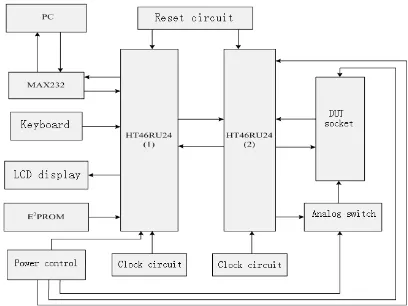
connection machine, and provide a powerful user interface and software resources. With the machine running, it can transfer the test vectors in PC program library to
Figure 1. The framework of system hardware design.
tester and the results of tests can be show on the PC-screen, and it can also show the whole contents of the truth table and the actual testing results. Meanwhile, it can also make programming on the new IC in the PC, and store the program data into the database. System hardware design framework is shown in Figure 1.
THE ESTABLISHMENT OF TEST SET
The Establishment of Test Set
Based on the statistics of more than 200 kinds of common chips with TTL74, 54 series and CMOS4000, 4500, less than 20-pin chips take up about 98% or more, and the pins of the chips have the same width. Therefore, We design the 20-pin locking socket, and do the following provisions: The first and the final pin of the tested chip will be kicked into the first and the twentieth pin of the 20-pin locking socket, for the top right feet is for the power supply (Vcc) and lower left corner is for the ground (GND). Through the statistics of the literature, The GND pin of 20-pin locking socket is probably on pin “7”,“8”,“9”,“10”,“12”,“20”, where “12” and “20”are irregular chip pins.
According to the designed 20-pin locking socket, the maximum pin of measured chip test is corresponding to the 20 feet of test socket, the minimum pin of measured chip is corresponding to “1” pin of test socket , and the middle part is replaced by the pin (NC) respectively. Therefore, the chips with less than 20pinscan be considered to be 20-pin chips to design the test vectors for testing.
a) For the power cord and ground of tested IC, it selects the word corresponding to "1";
b) For any empty pin, it selects the word corresponding to "1";
c) If the output pin of the tested IC is considered as a PIO input, then it selects
the word corresponding to "0";
d) If the input pin of the tested IC is considered as a PIO output, then it selects
the word corresponding to "1".
We use the H/L to define the pin logic level, that is “1 is high, 0 is low”. If it needs to add the test pulse, we use the CP provision to determine which pins are the plus added pins, Where “1” is the plus added pin and “o” is the pin without plus. If it doesn’t add the pulse, CP is not arranged [7].
Model Definition
The first “0” means TTL series and “1”represents CMOS series. And the later three chip models represent hundred, ten, one.
I/O Control Word and Test Group Number
The provisions show the addresses are 62H, 63H, 64H, 64H, where the number in low 4 bits is the number of chip testing.
Grounding Definition
Analog switch and Software controlled ground wire are stored into the address “65H” in the RAM as follows.
00H:“7”ground pin; 01H: “8”ground pin; 02H: 9 ground pin; 03H:“10”ground pin.
Pulse Definition
After adding the I/O control words, we must consider whether it needs to add the pulse, and when the program will finish. Therefore, the design of the CP control words are placed in the address “66H” in RAM.
SOFTWARE SYSTEM DESIGN
operator that the machine is ready to receive keyboard input. When the prompt appears on the display, the keyboard scan subroutine is immediately transferred to the system. And then, the operator can input data or commands through the keyboard, the value is scanned and read back for key analysis to determine whether the key pressing is the number key or function key. If it’s the number key, the data correspond with key number will be sent to the display buffer and be displayed. Otherwise, if it’s a function key, the program will be transferred to the handling procedures with the corresponding function key. And then it returns to the display program. The system repeats the process after the computer is switched on.
Known-types Chip Testing
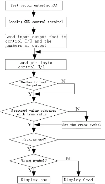
[image:6.612.219.392.354.657.2]For the known-type digital integrated circuits, when the chip type is input, the program will call different subroutine according to the different types of the chip, which is to add different combinations of high and low signal depending on the chip type in its input. And then, the output level signal is read to determine whether it’s the good or bad chip by judging correct logic function. The flow chart of known-types chip testing procedures is shown in Figure 2.
Unknown-types Chip Testing
For unknown-type chip which is not clear digital circuit chip, and it’s more difficult for analysis and testing than the known-type chip testing. For the ordinary chips, besides power and ground, there are input, output and control terminal, which control terminal can be used as input. To analyze the chip's logic function, the concrete steps are as follows:
Step 1: Determine that which is the input and which is the output.
Test method: Assume that a terminal is for the output, the computer chip under test will add all the other combinations of input signals through the program each other terminal (If the number of input is m, there are 2m times combinations[9]). In each case of input signal, the output level changes in the assumed output are tested. For all input combinations, if the level in assumed output of tests is constant, the hypothesis does not hold, which is that the assumed output is actually the input[10].In the m-inputs with different signal, once the level of the assumed output by testing has changed, then the assumption is true, which is that the assumed terminal is indeed the output of the chip. And then, the other pins on the chip under test have been tested with the same method until all the characters of input and output pins of the chip are clear.
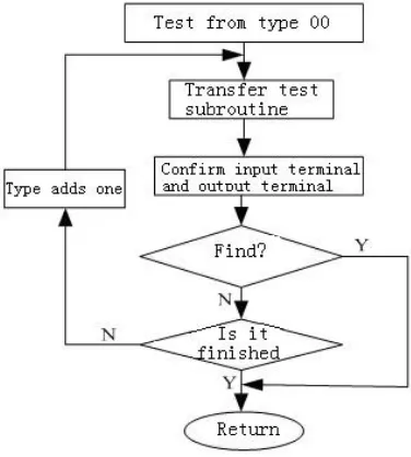
Step 2: Determine the type.
[image:7.612.210.398.416.625.2]On the one hand, the host is given the display model; on the other hand, the testing procedures with known-type chips is given to achieve the chip testing.
TESTING AND CONCLUSION
To test the reliability of the test instrument, we select the common CMOS, TTL chips for testing and verification, including 5CMOS chips, 5TTL series chips. In the system, it’s assumed that there are various conditions such as power failure, earth fault, input pin failure, the output pin failure, and the normal. By the actual test with the tester, it can accurately detect whether the chip is normal or not, and can also pinpoint the fault chip pin. In tests, 100% of the selected test samples are correct.
After testing and practical application, it shows that the chip testers occupy less hardware resources, and have a good man-machine interface. And it’s cheap and easy to carry, to be operated, can be used in the simple functional test of digital IC at any time. Therefore, it can be widely used in electronic product development, test, production, maintenance and other fields, having a good value. In the long-term plans, increasing the types of test chips is imperative. In order to make the performance of tester to be more perfect, the test chip interface can be extend through the I2C serial interface, and increase capacity of testing set of the chip and expand other functions.
REFERENCES
1. Yue Zhao, Fault Detecting System of Digital Integrated Circuit Board [J]. Journal of Liaoning Institute of Technology, 2003, 23(1):29-31.
2. Shi Yan, Digital Electronic Technology Foundation[M].Beijing: Higher Education Press, 2004. 3. Xibiao Cai. Testing System of Digital Integrated Circuit[D]. Journal of Liaoning Institute of
Technology, 2005.
4. Yue Zhao, Yiqian Tang, Xibiao Cai. Digital ICs Trouble Testing System[J]. Chinese Journal of Scientific Instrument, 2006.27(6):3-16.
5. Miron Abramovici, Melvin A. Breuer, Arthur D. Friedman. Digital Systems Testing and Testable Design[M], Beijing:China Machine Press, 2006.
6. Niraj Jha, Sandeep Gupta. Digital Systems Testing[M],Beijing: Publishing House of Electronics Industry, 2007.
7. Qiren Zhong. HT46xx IC’s Principle and Practice[M],Beijing: Publishing House of Beijing University of Aeronautics and Astronautics, 2008.
8. Zhiwei Huang. Training Course of National University Student Electron Design Competition[M], Beijing: Publishing House of Electronics Industry, 2005.