::E
N
o
~a.
o
[image:1.487.44.435.78.595.2]o
...
N
o
~a.
o
o
~National
D
Semiconductor
COP402/COP402M ROMless N-Channel Microcontrollers
General Description
The COP402/COP402M ROMless Microcontrollers are members of the COPSTM family, fabricated using N-channel silicon gate MOS technology. Each part contains CPU, RAM, and I/O, and is identical to a COP420 device, except the ROM has been removed; pins have been added to out-put the ROM address and to inout-put ROM data. In a system, the COP402 or 402M will perform exactly as the COP420; this important benefit facilitates development and debug of a COP420; this important benefit facilitates development and debug of a COP420 program prior to masking the final part. These devices are also appropriate in low volume ap-plications, or when the program may require changing. The COP402M is identical to the COP402, except the MICRO-BUSTM interface option has been implemented.
The COP402 may also be used to emulate the COP410L, 411 L, or 420L by appropriately reducing the clock frequen-cy.
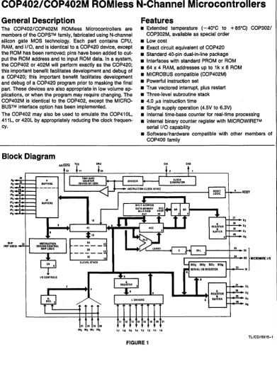
Block Diagram
,.
'1 IPJ I,. IPI 1P4 1P3 IPz IPI IPI
IKIP CNDTUIEDI
J4
,
31
I IUFFERS
31
IP BUFfERS
AD/iiilA
lJ
HEVELSTACK
Features
• Extended temperature ( - 40·C to
+
a5·C) COP302/ COP302M, available as special order• Low cost
• Exact circuit equivalent of COP420 • Standard 40-pin dual-in-line package • Interfaces with standard PROM or ROM • 64 x 4 RAM, addresses up to 1 k x a ROM • MICROBUS compatible (COP402M) • Powerful Instruction set
• True vectored interrupt, plus restart • Three-level subroutine stack • 4.0
,..,S
instruction time• Single supply operation (4.5V to 6.3V)
• Internal time-base counter for real-time processing • Internal binary counter register with MICROWIRETM
serial
110
capability• Software/hardware compatible with other members of COP400 family
r---+..t:...-:J--~
'"
\I IZ 1314 .. II ZD ZI ZJ 1.15 ZI
IN3 INZ INI IND
FIGURE 1
COP402/COP402M and COP302/COP302M
Absolute Maximum Ratings
If Mllltaryl Aerospace specified devices are required, Package Power Dissipation 750 mW at 25°C
contact the National Semiconductor Sales Offlcel 400 mW at 70°C
Distributors for availability and specifications. 250 mW at 85°C
Voltage at Any Pin -0.3Vto +7V Total Sink Current 50 rnA
Operating Temperature Range Total Source Current 70 rnA
COP402/COP402M O°Cto 70°C Note: Absolute maximum ratings indicate limits beyond
Storage Temperature Range - 65°C to + 150°C which damage to the device may occur. DC and AC
electri-lead Temperature (soldering, 10 sec.) 300°C cal specifications are not ensured when operating the
de-vice at absolute maximum ratings.
COP402/COP402M
DC Electrical Characteristics
O°C~
T A~
70°C, 4.5Vs:
Vee~
6.3V unless otherwise notedParameter Conditions Min Max Units
Operation Voltage 4.5 6.3 V
Power Supply Ripple Peak to Peak (Note 3) 0.4 V
Supply Current All Outputs Open Vee
=
5V 40 rnAInput Voltage levels CKllnput levels
Crystal Input
logic High 2.4 V
logic low -0.3 0.4 V
Schmitt Trigger Input RESET
logic High 0.7 Vee V
logic low -0.3 0.6 V
All Other Inputs
logic High Vee
=
Max 3.0 Vlogic High Vee
=
5V ±5% 2.0 Vlogic low -0.3 0.8 V
Input load Source Current Vee
=
5V, VIN=
OV -100 -800 p.AInput Capacitance 7 pF
Hi-Z Input leakage Vee
=
5V -1 +1 p.AOutput Voltage levels
0, G, l, SK, SO Outputs
TTL Operation Vee
=
5V ±10%logic High IOH
=
-100 p.A 2.4 Vlogic low IOL
=
1.6mA -0.3 0.4 VIPO-IP7, P8, P9, SKIP, CKO, AD/DATA
logic High IOH
=
-75 p.A 2.4 Vlogic low IOL
=
400 p.A -0.3 0.4 VCMOS Operation (Note 1)
logic High IOH
=
-10 p.A Vee -1 Vlogic low IOL
=
10 p.A -0.3 0.2 VOutput Current levels
lED Direct Drive (COP402) Vee
=
6Vlogic High VOH
=
2.0V 2.5 14 rnATRI-STATE® (COP402M) leakage Current Vee
=
5V -50 +50 p.AAllowable Sink Current
Per Pin (l, 0, G) 10 rnA
Per Pin (All Others) 2 rnA
Per Port (l) 16 rnA
PerPort(D,G) 10 rnA
Allowable Source Current
Per Pin (l) -15 rnA
Per Pin (All Others) -1.5 rnA
Note 1: TRI-STATE and LED configurations are excluded.
o
"0
"'"
o
III)...
o
o
"0
"'"
::E
N
o
v
Q.
o
o
...
N
o
v
Q.o
o
COP402/COP402M
AC Electrical Characteristics
o·c
s:
T As:
70·C,4.5Vs:
Vees:
6.3V unless otherwise notedParameter Conditions Min Max Units
Instruction Cycle Time 4 10 ,."s
Operating CKI Frequency + 16 Mode 1.6 4.0 MHz
CKI Duty Cycle (Note 1) 40 60 %
Rise Time Frequency
=
4 MHz 60 nsFall Time Frequency
=
4 MHz 40 nsInputs: SI
tSETUP 0.3 ,."s
tHOLO 250 ns
All Other Inputs
tSETUP 1.7 ,."s
tHOLO 300 ns
Output Propagation Delay Test Conditions:
RL
=
5k, CL=
50 pF, VOUT=
1.5V SOandSKtpd1 1.0 ,."s
tpdO 1.0 ,."s
CKO
tpd1 0.25 ,."s
tpdO 0.25 ,."s
AD/DATA, SKIP
tpd1 0.6 ,."s
tpdO 0.6 ,."s
All Other Outputs
tpd1 1.4 ,."s
tpdO 1.4 ,."s
MICROBUS Timing CL
=
100 pF, Vee=
5V ±5%Read Operation (Figure 4)
Chip Select Stable before RD-teSR 65 ns
Chip Select Hold Time for RD-tRes 20 ns
RD Pulse Width-tRR 400 ns
Data Delay from RD-tRO 375 ns
RD to Data Floating-toF 250 ns
Write Operation (Figure 5)
Chip Select Stable before WR-tesw 65 ns
Chip Select Hold Time for WR-twes 20 ns
WR Pulse Width-tww 400 ns
Data Set-Up Time for WR-tow 320 ns
Data Hold Time for WR-two 100 ns
INTR Transition Time from WR-twi 700 ns
Note 1: Duty Cycle = tWI/(tWl + two).
Note 2: See Figure 9 for additional I/O characteristics. Note 3: Voltage change must be less than O.SV in a 1 ms period.
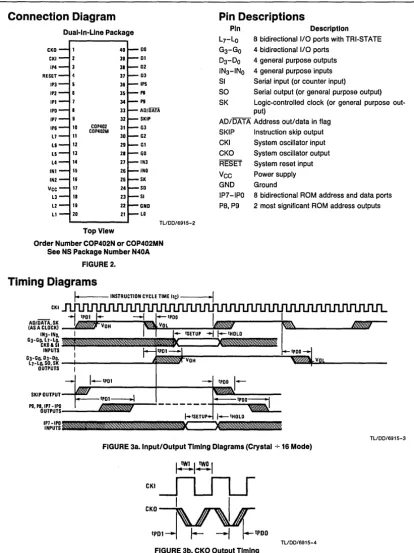
Connection Diagram
Pin Descriptions
Pin Description
Dual-In-Llne Package
L7-Lo G3- GO
03- 00
IN3-INo SI
8 bidirectional 1/0 ports with TAl-STATE
CKO CKI IP4 RESET IP3
40 00 39 01 31 02 37 03 36 IPS
4 bidirectional I/O ports
4 general purpose outputs
4 general purpose inputs Serial input (or counter input)
IP2 35 PI
IPI PI
IPO 33 AD/DATA
SO SK
Serial output (or general purpose output) Logic-controlled clock (or general purpose out-put)
IP7
IP6 10 COP402 COP402M 17 11 L8 12 L5 13
L4 14 INI 15 IN2 16
Vcc 17
SKIP
31 G3 AD/DATA Address out/data in flag
SKIP Instruction skip output
CKI System oscillator input
System oscillator output System reset input Power supply Ground
L3 18 L2 19
G2 GI GO IN3 INO SK SO SI GND LD
CKO RESET
Vee
GND IP7-IPO P8,P98 bidirectional ROM address and data ports
2 most significant ROM address outputs
LI 20 21
TL/DD/6915-2
Top View
[image:4.491.27.442.23.576.2]Order Number COP402N or COP402MN See NS Package Number N40A
FIGURE 2.
Timing Diagrams
I·
CKI
G3-Go. 03-00. L7-Lo.SO.SK _...J~
______
~--,~~~~iiiii---:'~~~ ~~"".11.1100______ _
OUTPUTS
- tPDO
1-SKIP OUTPUT t P D I - . !PI. Pl6~lp~;~
____
",fAIljWIlj$Ilj~"'~Ilj.W/lrgFIGURE 3a. Input/Output Timing Diagrams (Crystal + 16 Mode)
~I~I
CKI~
c,o~~r
'po,
~
l=
---:r
~
lPOOFIGURE 3b. CKO Output Timing
TLlDD/6915-4
TL/DD/6915-3
o
"U
~
o
I\)
...
o
o
"U
~
o
:IE
N
o
-.:t Q.
o
o
'"
No
-.:t Q.
o
o
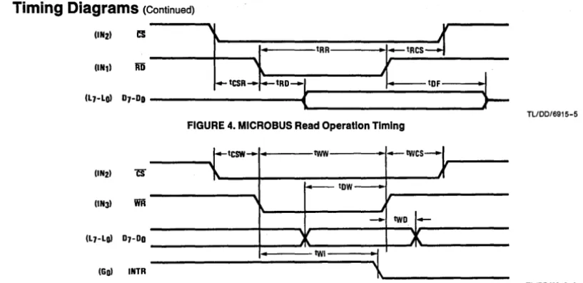
Timing Diagrams
(Continued),
I
,-I
t R R - - -...~J_tRCS::::j
---~--~\I
Ir---~---(lN1) fiIj J
~tcsR-t=:=tRO-
_ t O F - - -•.,J
(L7-LO) 07- 0D [image:5.491.47.456.34.232.2]---t(Ir---...;.---"\Ir--TL/DD/6915-5
FIGURE 4. MICROBUS Read Operation Timing
tcsw- • twW • - t w c s - /
(JN2)
cs
\.
I
~tow-(lN3) WR
-
two1-(L7-Lo! 07- 00
X
.
twl~
(Go) INTR
TLlDD/6915-6
FIGURE 5. MICROBUS Write Operation Timing
Functional Description
A block diagram of the COP402 is given in Figure 1. Data paths are illustrated in simplified form to depict how the vari-ous logic elements communicate with each other in imple-menting the instruction set of the device. Positive logic is used. When a bit is set, it is a logic "1" (greater than 2V). When a bit is reset, it is a logic "0" (less than 0.8V).
PROGRAM MEMORY
Program Memory consists of a 1,024-byte external memory (typically PROM). Words of this memory may be program instructions, program data or ROM addressing data. Be-cause of the special characteristics associated with the JP, JSRP, JID and LaiD instructions, ROM must often be thought of as being organized into 16 pages of 64 words each.
ROM addressing is accomplished by a 10-bit PC register. Its binay value selects one of the 1,024 8-bit words contained in ROM. A new address is loaded into the PC register during each instruction cycle. Unless the instruction is a transfer of control instruction, the PC register is loaded with the next sequential 10-blt binary count value. Three levels of sub-routine nesting are implemented by the 10-bit subsub-routine save registers, SA, SB and SC, providing a last-in, first-out (LIFO) hardware subroutine stack.
ROM instruction words are fetched, decoded and executed by the Instruction Decode, Control and Skip Logic circuitry.
DATA MEMORY
Data memory consists of a 256-bit RAM, organized as 4 data registers of 16 4-bit digits. RAM addressing is imple-mented by a 6-bit B register whose upper 2 bits (Br) select 1 of 4 data registers and lower 4 bits (Bd) select 1 of 16 4-bit digits in the selected data register. While the 4-bit contents of the selected RAM digit (M) is usually loaded into or from, or exchanged with, the A register (accumulator), it may also be loaded into or from the a latches or loaded from the L ports. RAM addressing may also be performed directly by the LDD and XAD instruction based upon the 6-bit
contents of the operand field of these instructions. The Bd register also serves as a source register for 4-bit data sent directly to the 0 outputs.
INTERNAL LOGIC
The 4-bit A register (accumulator) is the source and desti-nation register for most liD, arithmetic, logic and data mem-ory access operations. It can also be used to load the Br and Bd portions of the B register, to load and input 4 bits of the B·bit a latch data, to input 4 bits of the 8-bit L I/O port data and to perform data exchanges with the SID register. A 4-blt adder performs the arithmetic and logic functions of the COP402/402M, storing its results in A. It also outputs a carry bit to the 1-bit C register, most often employed to indicate arithmetic overflow. The C register, in conjunction with the XAS instruction and the EN register, also serves to control the SK output. C can be outputted directly to SK or can enable SK to be a sync clock each instruction cycle time. (See XAS instruction and EN register description, be-low.)
Four general-purpose Inputs, IN3-INo, are provided; IN1, IN2, and IN3 may be selected, by a mask-programmable option, as Read Strobe, Chip Select and Write Strobe in-puts, respectively, for use in MICROBUS applications. The 0 register provides 4 general-purpose outputs and is used as the destination register for the 4-bit contents of Bd. The G register contents are outputs to 4 general-purpose bidirectional 110 ports. Go may be mask-programmed as a
"ready" output for MICROBUS applications.
The Q register is an internal, latched, 8-bit register, used to hold data loaded to or from M and A, as well as 8·bit data from ROM. Its contents are output to the L 110 ports when
the L drivers are enabled under program control. (See LEI instruction.) With the MICROBUS option selected, a can also be loaded with the 8-bit contents of the L 110 ports
Functional Description
(Continued) The 8 L drivers, when enabled, output the contents of latched a data to the L I/O ports. Also, the contents of L may be read directly into A and M. As explained above, the MICROBUS option allows L I/O port data to be latched into the a register. L I/O ports can be directly connected to the segments of a multiplexed LED display (using the LED Di-rect Drive output configuration option) with a data being outputted to the Sa-Sg and decimal point segments of the display.The 510 register functions as a 4-bit serial-in/serial-out shift register or as a binary counter depending on the con-tents of the EN register. (See EN register description below.) Its contents can be exchanged with A, allowing it to input or output a continuous serial data stream. SIO may also be used to provide additional parallel I/O by connecting SO to external serial-in/parallel-out shift registers. The XA5 Instruction copies C into the SKL latch. In the counter mode, SK is the output of SKL. In the shift register mode, SK outputs SKL AN Oed with internal instruction cycle clock.
The EN register is an internal 4-bit register loaded under program control by the LEI instruction. The state of each bit of this register selects or deselects the particular feature associated with each bit of the EN register (EN3-ENo). 1. The least significant bit of the enable register. ENo.
se-lects the SIO register as either a 4-bit shift register or a 4-bit binary counter. With ENo set, SIO is an asynchro-nous binary counter, decrementing its value by one upon each low-going pulse ("1" to "0") occurring on the SI input. Each pulse must be at least two instruction cycles wide. SK outputs the value of SKL. The SO output is equal to the value of EN3. With ENo reset, SIO is a serial shift register shifting left each instruction cycle time. The data present at SI goes into the least significant bit of SIO. SO can be enabled to output the most significant bit of SIO each cycle time. (See 4 below.) The SK output becomes a logic-controlled clock.
2. With EN1 set the IN1 input is enabled as an interrupt in-put. Immediately following an interrupt, EN1 is reset to disable further interrupts.
3. With EN2 set, the L drivers are enabled to output the data in a to the L I/O ports. Resetting EN2 disables the L drivers, plaCing the L I/O ports in a high-impedance input state. If the MICROBUS option is being used, EN2 does not affect the L drivers.
4. EN3, in conjunction with ENo, affects the SO output. With ENo set (binary counter option selected) SO will output the value loaded into EN3.· With ENo reset (serial shift register option selected), setting EN3 enables SO as the output of the SIO shift register, outputting serial shifted data each instruction time. Resetting EN3 with the serial
shift register option selected disables SO as the shift reg-ister output; data continues to be shifted through SIO and can be exchanged with A via an XAS instruction but SO remains reset to "0." The table below provides a summa-ry of the modes associated with EN3 and ENo.
INTERRUPT
The following features are associated with the IN1 interrupt procedure and protocol and must be considered by the pro-grammer when utilizing interrupts.
a. The interrupt, once acknowledged as explained below, pushes the next sequential program counter address (PC
+
1) onto the stack, pushing in turn the contents of the other subroutine-save registers to the next lower level(PC
+
1 ~ SA ~ SB ~ SC). Any previouscon-tents of SC are lost. The program counter is set to hex address OFF (the last word of page 3) and EN1 is reset. b. An interrupt will be acknowledged only after the following
conditions are met: 1. EN1 has been set.
2. A low-going pulse ("1" to "0") at least two instruction cycles wide occurs on the IN1 input.
3. A currently executing instruction has been completed. 4. All successive transfer of control instructions and suc-cessive LBls have been completed (e.g., if the main program is executing a JP instruction which transfers program control to another JP instruction, the interrupt will not be acknowledged until the second JP instruc-tion has been executed.
c. Upon acknowledgement of an interrupt, the skip logic status is saved and later restored upon the popping of the stack. For example, if an interrupt occurs during the exe-cution of ASC (Add with Carry, Skip on Carry) instruction which results in carry, the skip logic status is saved and program control is transferred to the interrupt servicing routine at hex address OFF. At the end of the interrupt routine, a RET instruction is executed to "pop" the stack and return program control to the instruction following the original ASC. At this time, the skip logic is enabled and skips this instruction because of the previous ASC carry. Subroutines and the LaiD instruction should not be nest-ed within the interrupt servicing routine since their pop-ping of the stack enables any previously saved main pro-gram skips, interfering with the orderly execution of the interrupt routine.
d. The first instruction of the interrupt routine at hex address OFF must be a NOP.
e. An LEI instruction can be put immediately before the RET to re-enable interrupts.
TABLE I. Enable Register Modes-Bits EN3 and ENo
EN3 ENo 510 51 50 5K
0 0 Shift Register Input to Shift Register 0 If SKL
=
1, SK = SYNCIf SKL
=
0, SK = 01 0 Shift Register Input to Shift Register Serial Out If SKL
=
1. SK = SYNCIf SKL
=
0, SK = 00 1 Binary Counter Input to Binary Counter 0 If SKL
=
1, SK = 1If SKL
=
0, SK = 01 1 Binary Counter Input to Binary Counter 1 If SKL
=
1, SK = 1IfSKL
=
O,SK = 0o
-a
~ o N
...
o
o
-a
~
o
N
:e
N
Q "lilt'
a..
o
[image:7.492.259.457.48.501.2] [image:7.492.263.452.48.197.2]o
...
N
Q "lilt'
a..
o
o
Functional Description
(Continued)MICROBUS INTERFACE
The COP402M can be used as a peripheral microprocessor device, inputting and outputting data from and to a host mi-croprocessor (J-LP). IN1, IN2, and IN3 general purpose inputs become MICROBUS compatible read-strobe, chip-select, and write-strobe lines, respectively. IN1 becomes RD-a logic "0" on this input will cause Q latch data to be enabled to the L ports for input to the J-LP. IN2 becomes C8-a logic "0" on this line selects the COP402M as the J-LP peripheral device by enabling the operation of the RD and WR lines and allows for the selection of one of several peripheral components. IN3 becomes WR-a logic "0" on this line will write bus data from the L ports to the Q latches for input to the COP402M. Go becomes INTR, a "ready" output reset by a write pulse from the J-LP on the WR line, providing the "handshaking" capability necessary for asynchronous data transfer between the host CPU and the COP402M. This option has been designed for compatibility with Nation-al's MICROBU8-a standard interconnect system for 8-bit parallel data transfer between MOS/LSI CPUs and interfac-ing devices. (See MICROBUS, National Publication.) The functioning and timing relationships between the COP402M signal lines affected by this option are as specified for the MICROBUS interface, and are given in the AC electrical characteristics and shown in the timing diagrams (Figures 4 and 5). Connection to the MICROBUS is shown in Figure 6.
MICROPROCESSOR
RESET
~
RElET
INTERRUPT IINTR) Go
A a·BIT DATA BUS .... 1 " ___ 00 ... -_07 __ --..,, LO- L 7
... ". COP402M READ STROBE 1M)
CHIP SElECT (CS) IN1 INZ WRITE STROBE (\VA).. IN3
RESET
+
TL/DD/6915-7
FIGURE 6. MICROBUS Option Interconnect
INITIALIZATION
The Reset Logic will initialize (clear) the device upon power-up if the power spower-upply rise time is less than 1 ms and great-er than 1 J-Ls. If the powgreat-er supply rise time is greatgreat-er than 1 ms, the user must provide an external RC network and di-ode to the RESET pin as shown below. The RESET pin is configured as a Schmitt trigger input. If not used it should be connected to Vee. Initialization will occur whenever a logic "0" is applied to the RESET input, provided it stays low for at least two instruction cycle times.
Upon initialization, the PC register is cleared to 0 (ROM ad-dress 0) and the A, B, C, 0, EN, G, and SO are cleared. The SK output is enabled as a SYNC output, providing a pulse each instruction cycle time. Data Memory (RAM) is not
cleared upon initialization. The first instruction at address 0
must be a CLRA.
P + j
0 ... ~
-:-W vcc
E
:~ ~~
COP402/402M R
S IfEffi
U P
:::::
P GNO
L
V -
I
RC ~ 5 x Power Supply Rise Time TL/DD/6915-8
FIGURE 7. Power-Up Clear Circuit
OSCILLATOR
There are two basic clock oscillator configurations available as shown by Figure 8.
a. Crystal Controlled Oscillator. CKI and CKO are con-nected to an external crystal. The instruction cycle time equals the crystal frequency divided by 16.
b. External Oscillator. CKI is driven by an external clock signal. The instruction cycle time is the clock frequency divided by 16.
A
C~ CKO
t
.Io~~ .Io~~
r"4'D~
Crystal Value
4MHz
3.58 MHz
R1
1k
1k
..ru-EXTERNAL CLOCK
NOT USED
TL/DD/6915-9
Component Values
R2
C
1M 27 pF
1M 27pF
2.09 MHz 1k 1M 56pF
FIGURE 8. COP402/402M Oscillator
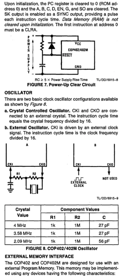
EXTERNAL MEMORY INTERFACE
The COP402 and COP402M are designed for use with an external Program Memory. This memory may be implement-ed using any devices having the following characteristics: 1. random addressing
2. TIL-compatible TRI-STATE outputs 3. TIL = compatible inputs 4. access time = 1.0 J-Ls, max.
Functional Description
(Continued) During operation, the address of the next instruction is sent out on P9, P8, and IP7 through IPO during the time that AD/DATA is high (logic "1" = address mode). Address data on the IP lines is stored into an external latch on the high-to-Iow transition of the AD/DATA line; P9 and P8 are dedicated address outputs, and do not need to be latched. When AD/DATA is low (logic "0"=
data mode), the output of the memory is gated onto IP7 through IPO, forming the input bus. Note that the AD/DATA output has a period of one instruction time, a duty cycle of approximately 50%, and specifies whether the IP lines are used for address out-put or instruction inout-put. A simplified block diagram of the external memory interface is shown in Figure 9.P9
- p a COP402
~ AD/DATA IP7 -IPo
... /"11..
.A
a g ( DATA
...
~v"_+K
DI
LATCH a
Q
en en
~ 8 c c ~c(>'
V
AD - A7 DO - D7
~ CE
~ Aa MEMORY A9
[image:8.494.56.215.152.369.2]TLlDD/6915-10
FIGURE 9. External Memory Interface to COP402
INPUT IOUTPUT
COP402 outputs have. the following configurations, illustrat-ed in Figure 10.
a_ Standard-an enhancement-mode device to ground in conjunction with a depletion-mode device to Vee, com-patible with TIL and CMOS input requirements. b. High Drive-same as a. except greater current sourcing
capability.
c. Push-Pull-an enhancement-mode device to ground in conjunction with a depletion-mode device paralleled by an enhancement-mode device to Vee. This configuration has been provided to allow for fast rise and fall times when driving capacitive .Ioads.
d. LED Direct Drive-an enhancement-mode device to ground and to Vee, meeting the typical current sourcing requirements of the segments of an LED display. The sourcing device is clamped to limit current flow. These devices may be turned off under program control (see Functional Description, EN Register), placing the outputs in a high-impedance stat~ to provide required LED seg-ment blanking for a multiplexed display .
e. TRI-STATE Push-Pull-an enhancement-mode device to ground and Vee intended to meet the requirements associated with the MICROBUS option. These outputs are TRI-STATE outputs, allowing for connection of these outputs to a data bus shared by other bus drivers. f. Inputs have an on-chip depletion load device to Vee, as
shown in Figure 10t.
The above input and output configurations share common enhancement-mode and depletion-mode devices. Specifi-cally, all configurations use one or more of six devices (numbered 1-6, respectively). Minimum and maximum cur-rent (lOUT and VOUT) curves are given in Figure 10 for each of these devices.
The SO, SK outputs are configured as shown in Figure 10e. The D and G outputs are configured as shown in Agure 10a.
o
"tJ ~
o
N
...
o
o
"tJ ~ o
N
:E
N
Q ~
Q.
o
[image:9.492.44.470.30.623.2]o
...
NQ
l
o
o
Functional Description
(Continued) Note that when inputting data to the G ports, the G outputs should be set to "1". The L outputs are configured as inFigure 10d on the COP402. On the COP402M the L outputs
are as in Figure 10e.
An important point to remember if using configuration d with the L drivers is that even when the L drivers are disabled,
the depletion load device will source a small amount of cur-rent. (See Figure 11.)
IP7 through IPO outputs are configured as shown in Figure 10e; P9, PS, SKIP, and AD/DATA are configured as shown
in Figure 10b.
vee
c~
a. Standard
d.lED
(.I. is Depletion Device)
TL/DD/6915-11
TL/DD/6915-14
TL/DD/6915-12
b. High Drive
TL/DD/6915-15
e. TRI-STATE Push-Pull
FIGURE 10. Input/Output Configurations
TLlDD/6915-13
c. Push-Pull
vee
lNPUT&~
TL/DD/6915-18
Typical Performance Characteristics
:c .!
~
Output Sink Current 15~,r--r--r~r--r--r-~
2 3 4 5 VOUT (VOLTS) DEVICE 1
HIgh Drive Source Current
-10
-Ir-~--+--+--+--+--r-~
-11 -11 -14 -12 -10 -I
-I
-4 -2
4
VOUT (VOLTS) OEVICE 2h
LED Output Direct LED Drive
VOUT- 2.DV ; '
LfI'"
/
[image:10.487.30.438.54.585.2]" "
...
l -I"""'"u u
VCC (VOLTS) MAX ~'
.... V
~
..:t
8.5 OEVICE 4
-0.4
-0.3
~
-0.2~
-0. 1
Depletion Load OFF Source Current
1\
\
~MAX
MIN
\
D~'\.
VOUT (VOLTS) DEVICE 2
Push·Pull Source Current
VOUT (VOLTS) DEVICE 3
TRI-STATE
Output Source Current
i
-10 t+--f\--\-++-t--t-+--i~
2 3 4 5 VOUT (VOLTS) DEVICE 5
Standard Output Source
-2.0 Current
-1. 71 '--t---r--t---I--t--I-~
-1.5 k--::7'~F--r-'-r-+--t--J
!
-1.255 -1.0 rT~c:::...;.:;=-+~-'--t--i
~ -D. 75 k-~-r"oc:'-+-f--1r--t----1r--I -0.5 r---f"~r*lIoodf++-Ir--J -0.25 r--P"~!T-~....t!--""v--i----t
Vour (VOLTS) DEVICE 2
LED Output Source Current
-20
-11 -11 -14
1
-12~
-10~ -I -I
-4 -2
L"-.
I
I
I
\ VCC-uv
(MAX)I I
~
I I
""""'I
\.
:,..Vc -4.IV (MAX)l\rfo"'"
I I
\
,
1\
Vcc·uv
(MIN)V
I I
11 \ Vcc· 1.3V (MIN), -
IX
/I I
I'"
I"""'<-'"
~l'-J
I
VOUT (VOLTS) DEVICE 4
Input Load Current
FIGURE 11. COP402/COP402M Input/Output Characteristics TL/DD/6915-17
o
"tJ ~
o
I\)... (')
o
"tJ ~
o
I\):E
N Q ~ D.
o
o
...
N Q ~ D.
o
o
Typical Performance Characteristics
(Continued)15 Output Sink Current
10Hf-t---1I'~
2 3 4
VOUT (VOLTS) DEVICE 1
Standard Output Source Current
-1.75
-1.5 P'r-l~-.--=--r...!...1f--+-_+_--l
-1. 25 I---'t~:_'_---:-~-:-:-:-:':-:--+-_+_--l
!
-1.0 I-T-II'-'I.:-+---t---If--+-_+_--l....
§
-0.75 I---+ ... -+''r-+---If---+---+---l-0.5
3 4
L Output Depletion Load Off Source Current
<" -0.4
g ~ -0.3
N
..
<" E
-0.2
-0.1
~l\
4
VOUT (VOLTS) DEVICE 2
Push Pull Source Current
- 3.0 ,...---,-"TT'"'-r-r--.,--,,---r--,
- 2.5 I---ti--t--t-t-tt'-I="-=t----i - 2.0 f--++-+t--4+--4-!. ;: -1.5 f--+--l-PHH--.'+-I--+---i
§
-1.0 I----f)'--H-+-t---{.-I-'---'t----i
2 4
VOUT (VOLTS) DEVICE 2 AND 3
VOUT (VOLTS) DEVICE 2
LED Output Device LED Drive
...
g .... ::> ~
<" g
....
§
LED Output Source Current -24r-~---r--~--,...---r-~
-20
-16
-12
-B
2 3 4
VOUT (VOLTS)
5 6
DEVICE 4 AND 2
TRI·STATE Output Source Current
-15~-+--Hr_~,--r__+-:-+-____i
-10
-5
4
VOUT (VOLTS) DEVICE 5
,
-14
-12
/
/
-10
<" g
-B
.... ::> ~
MAX
/
/
-6,
,
VDUT = 2.0V
,
,
-4
,
-2
.-"
,..,-....
o
4.0 4.5 5.0 5.5 6.0
VCC (VOLTS) DEVICE 4 AND 2
Input Load Source Current
-1.0 1---+--+--+---1-'---+---1
-O.B
<" E
;: -0.6 I---"'d--rl----:-f---=''='''''''*=_-I
§
- 0.2 t---\:--t----'~-l"t.:--+-__I
2 3 4
[image:11.491.43.448.39.598.2]VOUT (VOLTS) DEVICE 6
Instruction Set
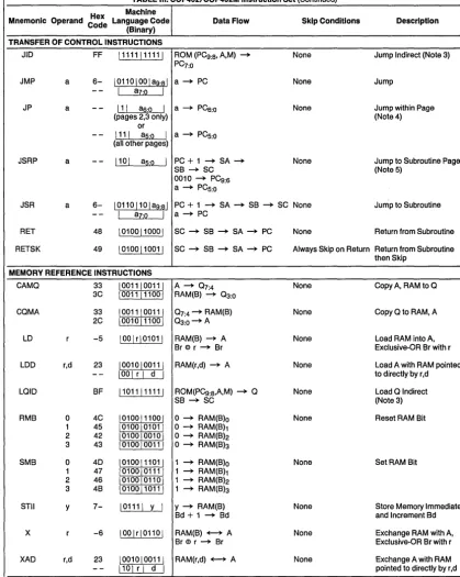
Table II is a symbol table providing internal architecture, in-struction operand and operational symbols used in the In-struction set table.
Table III provides the mnemonic, operand, machine code, data flow, skip conditions and description associated with each instruction in the COP402/402M instruction set.
TABLE II. COP402/COP402M Instruction Set Table Symbols
Symbol Definition Symbol Definition
INTERNAL ARCHITECTURE SYMBOLS INSTRUCTION OPERAND SYMBOLS
A 4-bit Accumulator d 4-bit Operand Field, 0-15 binary (RAM Digit Select)
8 6-bit RAM Address Register r 2-bit Operand Field, 0-3 binary (RAM Register
8r Upper 2 bits of 8 (register address) Select)
8d Lower 4 bits of 8 (digit address) a 9-bit Operand Field, 0-511 binary (ROM Address)
C 1-bit Carry Register y 4-bit Operand Field, 0-15 binary (Immediate Data)
o
4-bit Data Output Port RAM(s) Contents of RAM location addressed by sEN 4-bit Enable Register ROM(t) Contents of ROM location addressed byt
G 4-bit Register to latch data for G liD Port
IL Two 1-bit Latches Associated with the IN3 or
IN L M
INo inputs 4-bit Input port 8-bitTRI-STATE liD Port
4-bit contents of RAM Memory pointed to by 8 Register
OPERATIONAL SYMBOLS
+
PlusMinus Replaces Is exchanged with Is equal to
P PC
Q
2-bit ROM Address Port
10-bit ROM Address Register (program counter) 8-bit Register to latch data for L liD Port
A
Ell
The one's complement of A Exclusive-OR
SA S8 SC SID SK
1 O-bit Subroutine Save Register A 1 O-bit Subroutine Save Register 8 1 O-bit Subroutine Save Register C 4-bit Shift Register and Counter Logic-Controlled Clock Output
[image:12.491.26.443.85.598.2]Range of values
TABLE III. COP402/COP402M Instruction Set
Hex Machine
Mnemonic Operand
Code Language Code Data Flow Skip Conditions
(Binary)
ARITHMETIC INSTRUCTIONS
ASC 30 10011100001 A + C + RAM(8) --. A Carry
Carry --. C
ADD 31 1001110001
I
A + RAM(8) --. A NoneADT 4A 10100110101 A + 1010 --. A None
AISC Y 5- 10101 1 y
I
A+y--.A CarryCASC 10 10001100001 A + RAM(8) + C --. A Carry
Carry --. C
CLRA 00 10000100001 O--'A None
COMP 40 10100100001 A--'A None
NOP 44 10100101001 None None
RC 32 10011100101 "0" --. C None
SC 22 10010100101 "1" --. C None
XOR 02 10000100101 A Ell RAM(8) --. A None
Description
Add with Carry, Skip on Carry
Add RAM toA
Add Ten to A
Add Immediate, Skip on Carry (y =1= 0)
Complement and Add with Carry, Skip on Carry
Clear A
One's complement of A to A
No Operation
ResetC
SetC
Exclusive-OR RAM with A
o
"0
~
o
N
'"
o
o
"0
~
o
N
[image:12.491.26.443.96.598.2]:E
C'i
o ~
ID..
o
[image:13.491.39.459.59.584.2]o
...
C'i
o
~ID..
o
o
Instruction Set
(Continued)TABLE III. COP402/COP402M Instruction Set (Continued)
Mnemonic Operand
~oe:e
Machine
Language Code Data Flow Skip Conditions
(Binary)
TRANSFER OF CONTROL INSTRUCTIONS
JIO FF 1111111111
I
ROM (PC9:e, A,M) ~ NonePC7:0
JMP a 6- 10110
I
00I
a9"al a ~ PC None--
I
aZ"QI
JP a
--
11I
a!2"OI
a ~ PC6:0 None(pages 2,3 only) or
--
1111 a5"QI
a ~ PCs:o(all other pages)
JSRP a
--
110 1 a5"QI
PC+ 1 ~ SA ~ NoneSB ~ SC
0010 ~ PC9:6
a ~ PCs:o
JSR a 6- 10110110
I
a9"aI
PC + 1 ~ SA ~ SB ~ SC None--
I
aZ"QI
a ~ PCRET 48
I
0100 11000I
SC ~ SB ~ SA ~ PC NoneRETSK 49 10100110011 SC ~ SB ~ SA ~ PC Always Skip on Return
MEMORY REFERENCE INSTRUCTIONS
CAMO 33 1001110011
I
A ~ 07:4 None3C 10011111001 RAM (B) ~ 03:0
COMA 33 1001110011
I
07:4 ~ RAM(B) None2C 10010 11100
I
03:0~ALO r -5 100
I
rl01011 RAM (B) ~ A NoneBr ED r ~ Br
LOO r,d 23 1001010011
I
RAM(r,d) ~ A None--
1001 rI
dI
LOID BF 11011 11111
I
ROM(PC9:e,A,M) ~ 0 NoneSB ~ SC
RMB 0 4C 1010011100
I
o
~ RAM(B)o None1 45 1010010101
I
o
~ RAM(B)12 42 10100100101
o
~ RAM(B)23 43 1010010011
I
o
~ RAM(Bh5MB 0 40 1010011101
I
1 ~ RAM(B)o None1 47 1010010111
I
1 ~ RAM(B)12 46 10100101101 1 ~ RAM(B)2
3 4B 1010011011
I
1 ~ RAM(BhSTII y 7- 10111 1 y
I
y ~ RAM (B) NoneBd + 1 ~ Bd
X r -6 100
I
rI
0110I
RAM (B) +-+ A NoneBr ED r ~ Br
XAD r,d 23 1001010011
I
RAM(r,d) +-+ A None--
110 1 rI
dI
Description
Jump Indirect (Note 3)
Jump
Jump within Page (Note 4)
Jump to Subroutine Page (Note 5)
Jump to Subroutine
Return from Subroutine
Return from Subroutine then Skip
Copy A, RAM to 0
Copy 0 to RAM, A
Load RAM into A, Exclusive-OR Br with r
Load A with RAM pointed to directly by r,d
Load 0 Indirect (Note 3)
Reset RAM Bit
Set RAM Bit
Store Memory Immediate and Increment Bd
Exchange RAM with A, Exclusive-OR Br with r
Instruction Set
(Continued)TABLE III. COP402/COP402M Instruction Set (Continued)
Hex Machine
Mnemonic Operand
Code Language Code Data Flow Skip Conditions
(Binary)
MEMORY REFERENCE INSTRUCTIONS (Continued)
XDS r -7 100 1 r 1 0111 1 RAM(B) ~ A Bd decrements past 0
Bd - 1 --. Bd Br EB r --. Br
XIS r -4 1 00 1 r 1 0100 1 RAM (B) ~ A Bd increments past 15
Bd
+
1 --. Bd Br EB r --. Br REGISTER REFERENCE INSTRUCTIONSCAB 50 10101100001 A --. Bd None
CBA 4E 10100111101 Bd --. A None
LBI r,d
--
1001rl(d -1)1 r,d --. B Skip until not a LBI(d=O, 9:15) or
33 10011100111
--
110 1 r 1 d 1(any d)
LEI y 33 10011 10011 1 y --. EN None
6- 10110 1 y
I
XABR 12 10001100101 A ~ Br (0,0 --. A3.A2) None
TEST INSTRUCTIONS
SKC 20 10010100001 C = "1"
SKE 21 10010100011 A = RAM (B)
SKGZ 33 10011100111 G3:0 = 0
21 10010100011
SKGBZ 33 10011100111 1st byte
0 01 10000100011
} 2nd byte
Go = 0
1 11 10001100011 G1 = 0
2 03 10000100111 G2 = 0
3 13 10001100111 G3 = 0
SKMBZ 0 01 10000100011 RAM(B)o = 0
1 11 10001100011 RAM(Bh = 0
2 03 10000100111 RAM(B)2 = 0
3 13 10001100111 RAM(Bb = 0
SKT 41 10100100011 A time-base counter
carry has occurred since last test
Description
Exchange RAM with A and Decrement Bd, Exclusive-OR Br with r
Exchange RAM with A and Increment Bd, Exclusive-OR Br with r
Copy A toBd
CopyBd toA
Load B Immediate with r,d (Note 6)
Load EN Immediate (Note 7)
Exchange A with Br
Skip if C is True
Skip if A Equals RAM
Skip if G is Zero (all 4 bits)
Skip if G Bit is Zero
Skip if RAM Bit is Zero
Skip on Timer (Note 3)
o
"'0 ~
o
N
...
o
o
"'0 ~
o
N
::E
C\I
C)
oe::t'
[image:15.494.37.461.40.321.2]a-0
(,)...
C\I
C)
oe::t'
a-0
(,)Instruction Set
(Continued)TABLE III. COP402/COP402M Instruction Set (Continued)
Machine Hex
Mnemonic Operand Language Code DataFlow Skip Conditions Description
Code
(Binary)
INPUT/OUTPUT INSTRUCTIONS
ING 33
10011100111
G ... A None Input G Ports to A2A
10010110101
ININ 33
10011100111
IN ... A None Input IN Inputs to A28
10010110001
(Notes 2 and 8)INIL 33
10011100111
ILs,"0",
ILo ... A None Input IL Latches to A29
10010110011
(Note 3)INL 33
10011100111
L7:4 ... RAM (B) None Input L Ports to RAM,A2E
10010111101
Ls:o ... A08D 33
10011100111
8d ... D None Output 8d to D Outputs3E
10011111101
OGI y 33
10011100111
y ... G None Output to G Ports Immediate5-
10101 1
~1
OMG 33
1001110011
I
RAM(8) ... G None Output RAM to G Ports3A
10011110101
XAS 4F
10100111111
A ~ SIO,C ... SKL None Exchange A with SIO(Note 3)
Note 1: All subscripts for alphabetical symbols indicate bit numbers unless explicitly defined (e.g., Br and Bd are explicitly defined). Bits are numbered 0 to N where
o
signifies the least significant bit (low-order, right-most bit). For example, A3 Indicates the most significant (left-most) bit of the 4-bit register. Note 2: The ININ instruction is not available on the 24-pin COP421 since this device does not contain the IN inputs.Note 3: For additional information on the operation of the XAS, JID, LaiD, INIL, and SKT instructions, see below.
Note 4: The JP instruction allows a jump, while in subroutine pages 2 or 3, to any ROM location within the two-page boundary of pages 2 or 3. The JP Instruction, otherwise, permits a jump to a ROM location within the current 64-word page. JP may not jump to the last word of a page.
Note 5: A JSRP transfers program control to subroutine page 2 (0010 is loaded into the upper 4 bits of Pl. A JSRP may not be used when in pages 2 or 3. JSRP may not jump to the last word in page 2.
Note 6: LBlls a single-byte instruction if d = 0,9,10,11,12,13,14, or 15. The machine code for the lower 4 bits equals the binary value of the "d" data minus 1, e.g., to load the lower four bits of B (Bd) with the value 9 (10012), the lower 4 bits of the LBllnstructlon equal 8 (10002). To load 0, the lower 4 bits of the LBI Instruction should equal 15 (11112).
Note 7: Machine code for operand field y for LEI instruction should equal the binary value to be latched Into EN, where a "1" or "0" in each bit of EN corresponds with the selection or deselection of a particular function associated with each bit. (See Functional Description, EN Register.)
Description of Selected
Instructions
The following information is provided to assist the user in understanding the operation of several unique instructions and to provide notes useful to programmers in writing pro-grams.
XAS INSTRUCTION
XAS (Exchange A with SIO) exchanges the 4-bit contents of the accumulator with the 4-bit contents of the SIO register. The contents of SIO will contain serial-in/serial-out shift reg-ister or binary counter data, depending on the value of the EN register. An XAS instruction will also affect the SK out-put. (See Functional Description, EN Register, above.) If SIO is selected as a shift register, an XAS instruction must be performed once evey 4 instruction cycles to effect a con-tinuous data stream.
JID INSTRUCTION
JID (Jump Indirect) is an indirect addressing instruction, transferring program control to a new ROM location pointed to indirectly by A and M. It loads the lower 8 bits of the ROM address register PC with the contents of ROM addressed by the 10-bit word, PCg:a, A, M. PCg and PCa are not affected by this instruction.
Note that JID requires 2 instruction cycles.
INIL INSTRUCTION
INIL (Input IL Latches to A) inputs 2 latches, IL3 and
11.0
(seeFigure 12) and CKO into A. The IL3 and
11.0
latches are set if a low-going pulse ("1" to "0") has occurred on the IN3 and INo inputs since the last INIL instruction, provided the input pulse stays low for at least two instruction times. Execution of an INIL inputs IL3 and INo into A3 and AO respectively, and resets these latches to allow them to respond to subse-quent low-going pulses on the IN3 and INo lines. If CKO is mask programmed as a general purpose input, an INIL will input the state of CKO into A2. If CKO has not been so programmed, a "1" will be placed in A2. A "0" is always placed in A 1 upon the execution of an INIL. The general purpose inputs IN3-INo are input to A upon the execution of an ININ instruction. (See Table III, ININ instruction.) INIL is useful in recognizing pulses of short duration or pulses which occur too often to be read conveniently by an ININ instruction.CDP420
ININ
1.
INo/lNa
INIL
TL/DD/6915-19
FIGURE 12. INoIIN3 Latches
LaID INSTRUCTION
LaiD (Load a Indirect) loads the 8-bit a register with the contents of ROM pointed to by the 1 O-bit word PCg, PCa, A, M. LaiD can be used for table lookup or code conversion such as BCD to seven-segment. The LaiD instruction "pushes" the stack (PC
+
1 -+ SA -+ SB -+ SC) and replaces the least significant 8 bits of PC as follows: A -+PC7:4, RAM (B) -+ PC3:0, leaving PCg and PCa
un-changed. The ROM data pointed to by the new address is fetched and loaded into the a latches. Next, the stack is "popped" (SC -+ SB -+ SA -+ PC), restoring the saved value of PC to continue sequential program execu-tion. Since LaiD pushes SB -+ SC, the previous contents of SC are lost. Also, when LaiD pops the stack, the previ-ously pushed contents of SB are left in SC. The net result is that the contents of SB are placed in SC (SB -+ SC). Note that LaiD takes two instruction cycle times to execute.
SKT INSTRUCTION
The SKT (Skip on Timer) instruction tests the state of an internal 10-bit time-base counter. This counter divides the instruction cycle clock frequency by 1024 and provides a latched indication of counter overflow. The SKT instruction tests this latch, executing the next program instruction if the latch is not set. If the latch has been set since the previous test, the next program instruction is skipped and the latch is reset. The features associated with this instruction, there-fore, allow the controller to generate its own time-base for real-time processing rather than relying on an external input signal.
For example, using a 2.097 MHz crystal as the time-base to the clock generator, the instruction cycle clock frequency will be 131 kHz (crystal frequency -;- 16) and the binary counter output pulse frequency will be 128 Hz. For time-of-day or similar real-time processing, the SKT instruction can call a routine which increments a "seconds" counter every 128 ticks.
INSTRUCTION SET NOTES
a. The first word of a program (ROM address 0) must be a CLRA (Clear A) instruction.
b. Although skipped instructions are not executed, one in-struction cycle time is devoted to skipping each byte of the skipped instruction. Thus all program paths take the same number of cycle times whether instructions are skipped or executed, except JID and LaiD. LaiD and JID take two cycle times if executed and one if skipped. c. The ROM is organized into 16 pages of 64 words each.
The Program Counter is a 10-bit bil'1ary counter, and will count through page boundaries. If a JP, JSRP, JID or LaiD instruction is located in the last word of a page, the instruction operates as if it were in the next page. For example: a JP located in the last word of a page will jump to a location in the next page. Also, a LaiD or JID located in the last word of page 3, 7, 11, or 15 will access data in the next group of 4 pages.
o
"'0
0l:Io
o
N
...
o
o
"'0
0l:Io
o
N
::E
~
Typical Application: PROM-Based System
D. The COP402 may be used to exactly emulate the COP420, When AD/DATA turns off, the EPROMs are enabled and
8
Figure 13 shows the interconnect to implement a COP420 the IP7·IPO pins will input the memory data. P8 and P9 out·~ hardware emulation. This connection uses two MM5204 put the most significant address bits to the memory. (SKIP
o
EPROMs as external memory. Other memory can be used output may be used for program debug if needed.):. such as bipolar PROM or RAM. The other 28 pins of the COP402 may be configured exactly
o
Pins IP7-IPO are bidirectional inputs and outputs. When the the same as a COP420. The COP402M chip can be used ifo
AD/DATA clocking output turns on, the EPROM drivers are the MICROBUS feature of the COP420 is needed.disabled and IP7-IPO output addresses. The 8·bit latch (MM74C373) latches the addresses to drive the memory.
Vee 24
Lll
Vee vpp GNO 12GNO 23
AI 1
A7
2 MM2758
.!!... GNO
A6 OR Y, OF AID 3A5 MM2716 4
A4
Vee
5 A3 B
A2 A9 22
7
AI DE ~
19 II 15 12 9 B I 5 r AD
a
~ Q8 Q7 QI Q5 Q4 Q3 Q2 Ql 07 DB 05 04 03 02 01 DO20
Vee 17 lB 15 14 13 11 10 9
~-tI
GNO DM74LS373 [ln
OUTPUT DIS
08 07 DB 05 04 03 02 01 18 17 14 13 8 7 14 13
9 10 36 3 5 6 7 8 33 34
35
PI IP7 IP6 IPS 1P4 IP3 IP2 IPI IPO AD/DATA P9
~
SKIP 4022 39
1 38
2 eOP402 37
4 31
11
.!L---l!
-13 14 15 16 17 18 19 20 21 23 24 25 2B 27 21 29
-COP420PINOUT \ 1 2 3 4 6 6
f
GNO CKO CKIRESET L7 L6 L5 L4 INI IN2 VCC L3 L2 Ll LO SI SO SK INO IN3 GO Gl G2 G3 03 02 01 DO 8 9 10 11 12 13 14 15 lB 17 18 19 20 21 22 23 2426 28 27 21 [image:17.492.45.455.120.597.2]TL/DD/6915-20
Option List
COP402 MASK OPTIONS
The following COP420 options have been implemented in this basic version of the COP402. Subsequent versions of the COP402 will implement different combinations of available options; such versions will be identified as COP402-A, COP402-B, etc.
Option Value Option 1 = 0 Option 2 = 0
Option 3 = 0
Comment Ground Pin-no option available CKO is clock generator output to crystal
CKI is crystal input + 16 (may be overridden externally)
Option 4 = 0 RESET pin has load device to
Vee
Option 5 = 2 (402) L7 has LED direct-drive output = 3 (402M) L7 has TRI-STATE push-pull output Option 6 = 2, 3
Option 7 = 2,3
L6 same as L7 L5 same as L7
Option 8 = 2,3 L4 same as L7
Option 9 = 0 (402) IN1 has load device to
Vee
= 1 (402M) Hi Z
Option 10 = 0 (402) IN2 has load device to
Vee
= 1 (402M) Hi Z Option 11 = 0
Option 12 = 2,3 Option 13 = 2,3 Option 14
=
2,3Vee
pin-no option available L3 same as L7L2 same as L7 L1 same as L7
Option Value Option 15 = 2,3
Comment LO same as L7
Option 16 = 0 SI has load device to
Vee
Option 17 = 2 SO has push-pull output
Option 18 = 2 SK has push-pull output
Option 19 = 0 INO has load device to
Vee
Option 20 = 0 (402) IN3 has load device to
Vee
= 1 (402M) Hi Z Option 21 = 0
Option 22 = 0 Option 23 = 0 Option 24 = 0 Option 25 = 0 Option 26 = 0 Option 27 = 0
GO has standard output G1 same as GO G2 same as GO G3 same as GO 03 has standard output 02 same as 03 01 same as 03
Option 28
=
0 DO same as 03Option 29 = 0 (402) normal operation
= 1 (402M) MICROBUS operation
Option 30 = N/A 40-pin package
o
"'U
0l=Io
o
N
'"
o
o
"'U
0l=Io
o
N
3: