Implementation of a 3-bit Flash ADC using
TIQ Modified Comparator Circuit and
NOR-ROM based Encoder
Swarupa B N1, Dr. Vijaya Prakash A M2, Kumaraswamy K V3
M.Tech Student (VLSI and ES), Dept. of ECE, Bangalore Institute of Technology, Bengaluru, India1
Professor, Dept. of ECE, Bangalore Institute of Technology, Bengaluru, India2
Technical Manager, Trident Techlabs Pvt. Ltd., Bengaluru, India3
ABSTRACT: Analog to digital converter is required to interface the analog signal with digital signal. In the proposed paper a 3-bit Flash ADC is implemented in 130nm technology. Threshold Inversion Quantization(TIQ) technique is used for the comparators. The TIQ based comparator technique reduces non linearity in case of process variations. Design is optimized for speed with accuracy. The usage of TIQ will reduce the complexity of design. A 3-bit and a 4-bit ADC is implemented in 130 nm technology. The design is done using active devices only. The power dissipation that is observed for the 3 bit ADC is 0.034 mW. The VLSB that can be obtained by the design is 0.68mV. The implementation of the design is done using Mentor Graphics EDA tool.
KEYWORDS: Threshold Inversion Quantization technique, Flash ADC
I.INTRODUCTION
The analog to digital converter is a device which converts a continuous physical quantity (voltage or current) into a discrete quantity or a digital number that represents the quantity’s amplitude. The conversion involves quantization of the input, which means sampling the amplitude, so it necessarily introduces a small amount of error. Furthermore, instead of continuously performing the conversion, an ADC does the conversion periodically, sampling the input. The result is a sequence of digital values that have been converted from a continuous-time and continuous-amplitude analog signal to a discrete-time and discrete-amplitude digital signal.
Flash ADC
Flash ADC is a type of analog to digital convertor which converts analog quantity into digital quantity. It is considered to be a high speed ADC since the comparison of the input voltage with all the reference voltages are done parallely. Whereas in all the other types of ADC the computation is done one after the other. But the area occupied by the flash ADC is more when compared to all the other types of ADCs since Flash ADC has 2n – 1 comparators for a n bit ADC. The comparator used in the conventional flash ADC is built using an operational amplifier. The operational amplifier has a lot of non-linearity in its variation and it is complex to design. There are a lot of parameters that one need to take care of while designing an Op-amp comparator circuit. Also the conventional Flash ADC makes use of a ladder of resistor string which is used to generate a range of reference voltages. These reference voltages are compared to the applied input voltages and a thermometer code equivalent of the analog input is obtained.
TIQ comparator
Using TIQ techniques inverters can be used as a comparator for high speed and low power consumption. In this comparison is done at a higher speed when compared to the conventional differential op-amp based comparator. The different threshold voltages can be generated by using inverters of different switching voltages. And this variation can be done by altering the threshold voltage by varying the dimensions that is the length and the width of the transistors in the inverter circuit.
One out of N code Generator
The one out of N code generator generates a 16 bit output which is the one hot code equivalent of the obtained thermometer code which appears at the output of the comparators. The one out of N code generator is designed using bubbled AND gate combinational block in which the output is high when the comparator output is close to the input voltage i.e., at the edge of high to low variation of the comparator output.
63 X 6 NOR – ROM based encoder
The encoder block which follows the one out of N code generator is used to perform encoding of 64 bit value into 6 bit binary equivalent. NOR-ROM based encoder uses lesser number of transistors when compared to mux-based encoder, fat tree encoder and all the other encoding techniques that has been implemented. Hence it consumes lesser area and lesser power.
II.RELATED WORKS
There are a few authors who have implemented on flash ADC. The least achievable power in the case of these papers is 1.08mW, 6mW and 26mW and 119mW. [5][6]
In one of the work the author explains an ultrahigh speed ADC has been designed using 2x1 multiplexer based encoder. It is a 4-bit ADC which works on a supply of 1.8 V designed and simulated using level 3 Spice models. It is built using 120nm technology.[3] It has a conversion rate as high as 4GS/s and hence is considered as an ultrahigh speed ADC. It has a DNL errors of -0.174 LSB to 0.256 LSB and a dynamic range from 500mV to 1110mV leading to a total of 600mV. The power consumed by the circuit as observed in the simulation result is about 6.2031mW. It has an offset error of 0.5V. Certain observations have been made by the author wherein a smaller variation in the supply voltage of order ±6mV can show a matched variation in the threshold voltage.
In another paper the author has designed a medium speed flash ADC is implemented using the Gray code block for encoding.[8] The implementation is done on UMC 0.18μm CMOS technology with a supply voltage of 1.8V. It is
found to have a sampling rate of 100MS/s and a power consumption of 1.08 mW. It is found to have an INL of 1.36 LSB and a DNL of 1.04 LSB. It has a signal to noise ratio SNDR of 23.59 dB and the effective number of bits (ENOB) of 3.62 bits. The figure of Merit is 0.87 pJ/conversion step. It has an SFDR of 34.64 dB.
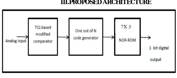
III.PROPOSED ARCHITECTURE
Figure 1.Block Diagram Of Proposed Architecture
The above figure describes the block diagram of the proposed flash ADC. An analog input signal is applied at the input of The TIQ based modified comparator block.
the switching voltage and if the applied input voltage is less than the switching voltage, the switching voltage being given by
……….(1)
……….(2)
Where, Vm denotes the switching voltage of the inverter circuit,
Vtp andVtn, the threshold voltage of PMOS and NMOS transistor respectively Cox, oxide capacitance
Vdd, supply voltage
µn and µp, mobility of electrons in NMOS and PMOS transistors respectively W and L, the width and length of the transistors.
The one out of N code generator generates a 16 bit output which is the one hot code equivalent of the obtained thermometer code which appears at the output of the comparators. The one out of N code generator is designed using bubbled AND gate combinational block in which the output is high when the comparator output is close to the input voltage i.e., at the edge of high to low variation of the comparator output.
The encoder block which follows the one out of N code generator is used to perform encoding of 16 bit value into 4 bit binary equivalent. NOR-ROM based encoder uses lesser number of transistors when compared to mux-basedencoder, fat tree encoder and all the other encoding techniques that has been implemented. Hence it consumes lesser area and lesser power.
IV.OPERATION OF TIQ BASED COMPARATOR
For the proposed Flash ADC TIQ based modified comparator has been used. The use of this type of comparator will eliminate the need to use a ladder of resistors to generate a set of reference voltage which is used for comparison with the input voltage.[7]
The MOSFET can be used as a switch by making it work in cutoff and active region or resistive region. If the gate to source voltage VGS is less than the threshold voltage, then the MOSFET will operate in cut off region and on the other hand if the gate to source voltage is greater than the threshold voltage, the transistor will operate in active region. Hence the threshold voltage of both the PMOS and NMOS together referred to as switching voltage of the inverter can be used as the reference voltage. [4]
V.SIMULATION RESULTS
TABLE 1: RESULTS AND SPECIFICATIONS
The table I explains the shows the specifications that are used when the circuit is being designed. The design is done in 130nm. The power dissipation observed in the circuit after simulation is 0.034mW for a supply voltage of 1V.
Figure 2. Transient Analysis of 3-bit flash ADC
The above graph explains the range of analog values which are converted to digital values using the analog to digital convertor. The minimum width of analog value which can be converted into digital value is shown.
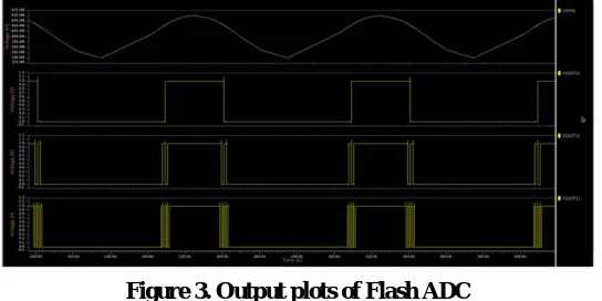
Figure 3. Output plots of Flash ADC
The figure 3 shows the simulation results for 3 bit TIQ based Flash ADC for a sinusoidal wave input.
VI.CONCLUSION AND FUTURE SCOPE
reduces the complexity of designing. Design is optimized for speed with accuracy. Using latest Architecture and implementing the ADC, considering all the performance parameters, a 4-bit Flash ADC with lower technology is implemented. Construction of ADC is done with only basic FETs using all active devices. The power dissipation for the implementation is 0.034 mW and 0.05mV for the 3-bit and 4-bit flash ADC respectively. The achievable VLSB is 0.68mV. The design can be further extended to higher resolution bit Flash ADCs.
REFERENCES
[1] Mostafa M. Ayesh, Sameh Ibrahim, Mohamed M. Aboudina,“A 15.5-mW 20 GSps 4-bit charge steering Flash ADC” IEEE, 2015
[2] Tretter, M. Khafaji, D. Fritsche, C. Carta, F. Ellinger G, “A 24 GS/s Single-Core Flash ADC with 3 Bit Resolution in 28 nm Low-Power Digital CMOS” IEEE, 2015
[3] Nazir, RoohieNaaz Mir, Najeeb-ud-din HakimLiyaqat, “A 4 GS/s,1.8 V Multiplexer encoder based Flash ADC using TIQ Technique”, 978-1-4799-2866-8/14, IEEE, 2014.
[4] Satya Narayan Mishra, WasimArif, JishanMehedi, SrimantaBaishya, “A Power Efficient 6-Bit TIQ ADC Design for Portable Applications”Third
International Conference on Consumer Electronics - Berlin (ICCE-Berlin),IEEE, 2013
[5] Timmy Sundstrom and AtilaAlvandpour ,"A 2.5-GS/s 30-mW 4-bit Flash ADC in 90nm CMOS," in 1-4244-2493-1/08 IEEE, 2008. [6] Jifang Wu, Fule Li, Weitao Li, Chun Zhang, and Zhihua Wang “A 14-bit 200MS/s Low-Power Pipelined Flash-SAR ADC”. [7] Daegyu Lee, JincheolYoo, and Kyusun Choi, “Design Method and Automation of Comparator Generation for Flash A/D Converter” [8] “A 4-bit medium speed Flash ADC using inverter based comparator in 0.18μm CMOS”, IEEE, 2015
[9] Inamdar, senior member, IEEE, Anubhavsahu, JieRen, SormehSetoodeh, Rafat Mansour, Deepa Narayan Gupta, “Design and evaluation of Flash ADC” IEEE