A Novel Approach to built an Area Efficient Architecture for Block
LDPC Codes
M.Devika
Lecturer, Department of Information Technology, Sathyabama University, Chennai, India.
Abstract—Low Density Parity Checker (LDPC) decoder requires large amount of memory access which leads to high energy consumption. The amount of achievable memory bypassing depends on the decoding orders of the layers. The proposed decoder was implemented in TSMC 0.18m CMOS process. Experimental results show that for a LDPC decoder targeting IEEE 802.11n specification, the amount of memory access values can be reduced by 12.9% to 19.3% compared with the state-of-the-art design. At the same time, 95.6% to 100% hardware utilization rate is achieved. The advantages of being able to test a variety of codes such those found in communications standards including Wireless LAN(IEEE 802.11n), WIMAX(IEEE 802.16e) and DVB-S2, on a single hardware platform will make the transition from theory to practice a much smoother one. The LDPC decoder design is flexible, it can accept a new code without any redesign , the only thing that changes is the ROM configuration. It has been tested, functionally verified and simulated with the MODELSIM tool by using VHDL code. Also the decoder has been show to operate correctly on larger codes and as performance demands increase, it has been show to scale up to larger design well. To understand, develop, the block of layers in LDPC decoder. It develops, implements and verifies in VHDL the correctly functioning LDPC decoder in VHDL implement and verify in VHDL code, a scheduling that allows the flexibility and as well as it configures by MODELSIM tool.
Keywords—LPDC decoder, VHDL, Check Nodes, Processor Nodes.
I. INTRODUCTION (Heading 1)
LOW-DENSITY parity-check (LDPC) block codes [1] are powerful linear error-correcting codes with decoding performance close to the Shannon capacity limit [2]. These codes have been considered for several recent digital communication standards such as the DVB-S2 [3], the IEEE 802.3an (10GBASE-T) [4], the IEEE 802.16e (WiMAX) [5], and the IEEE 802.11n (Wi Fi) [6] standards. LDPC codes are usually iteratively decoded by means of belief propagation [7] using message passing algorithms such as the Sum–Product Algorithm (SPA) or its less-complex approximation, the Min-Sum Algorithm (MSA) [8], with the expense of some
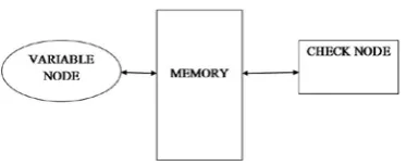
decoding loss. LDPC codes and their iterative decoding process can be graphically represented using bipartite factor graphs [9]. Factor graphs consist of two distinctive groups of nodes, variable nodes (VNs) and parity-check nodes (PNs).
The design, implementation and testing of a flexible Low Density Parity Check(LDPC) decoder built on Field Programmable Gate Array(FPGA) hardware has been studied in detail. The design and goal is to implement a flexible LDPC decoder that can handle different types of codes, enabling a variety of codes to be tested without redesigning the decoder. In LDPC, codes are a class of block code that satisfy both having a long length and randomness. These codes have the best performing up-to date , with their capacity of 0.0045 dB(Shannon limit). The performance is excellent while they are coupled with low decoding complexity that has seen LDPC codes includes in the standards for data transmission
such as Wi MAX(IEEE 802.16e), Digital Video
Broadcasting(DVB-S2) and as candidate for the new wireless LAN standard(IEEE 802.11n) and in emerging 3G evolution. One of the primary goals of the LDPC decoder in hardware is flexibility, enabling the above codes to be tested on a hardware platform, putting theory into practice. To integrate the decoder into Multiple Input Multiple Output(MIMO) communications are developing by A Tarrable et al’s[10].
A. Error Correction Coding
Errors are detected normally and corrected while communication takes place between a medium. It is the key part of the communication system, essential in our modern society. Compact disks, CD-ROM’s, DVS’s, mobile phones and hard disk drives all employ error correction coding to enable, reliable information transfer. [11] Shannon described the revolutionized communications with the limit, the proof is non-constructive; it only shows how the best possible codes will perform. In proving the channel capacity, he used random codes of infinite length; while these are not in practical that suggests the end of the encoding scheme.
B. Block Codes
Fig. 1. Serial Decoder Architecture
u = [u0 u1:::uki1] c = [c0 c1:::cni1]
An important parameter of a block code is its code rate(r). It is a measure of the amount of information (messages) bits sent per code word. If the error rate is low, amount of redundancy makes the transmitter to send the information with less time.
Serial decoder is the simplest decoder in terms of hardware cost shown in fig. 1. It consists of a single check node, a single variable node and memory. The variable nodes are updated in the same serial manner. This is the type of implementation that would arise from writing code that simply implements the sum of product algorithm either on a computer or as for a soft core on an FPGA. The main advantage of a serial implementation is that it is very flexible, supporting different block sizes and code rates, with only a new parity matrix to be loaded into memory. Unfortunately this approach is too slow for anything except simulations. The number of clock cycles required for each iteration of the serial decoder is approximately the twice number of edges.
A number of papers detailed methods to simplify the decoding process of LDPC codes by a specific design of the parity check matrix. By enforcing restrictions on the types of codes supported the decoder can simplified by exploiting the properties of the code such as regularity of the parity check matrix reducing its storage requirements on the decoder [12]. Hardware aware(collision free codes) can also be designed to eliminate collisions found in partially parallel architectures and achieve high throughputs[13]. The key goal of this paper is to implement a flexible LDPC decoder, designing a decoder based on specific code design techniques and restricting the types of supported codes to a greatly reduced subset would not meet the specifications of the project that may compensate in the future work.
II. RELATED WORKS
Based on [14], the energy-area optimal architecture for Gb/s data rates is highly parallel. In this regime memory-based designs are suboptimal because there are a large number of small, inefficient memory banks. On the other hand, fully pipelined architectures store messages in pipeline registers,which have no issue with overhead or bandwidth restrictions. Although the registers consume significant power, they are more efficient than memory blocks at the targeted rates. For this reason, only fully pipelined designs are considered.[15]presents a hardware architecture for fully
parallel stochastic low-density parity-check (LDPC) decoders. To obtain the characteristics of the proposed architecture, we apply this architecture to decode an irregular state-of-the-art (1056,528) LDPC code on a Xilinx Virtex-4 LX200 field-programmable gate-array (FPGA) device.
Hao Zhang[16] presents a silicon area efficient quasi cyclic (QC) low-density parity-check (LDPC) code decoder design solution, which is geared to magnetic recording that demands high code rate and very high decoding throughput under stringent silicon cost constraint. The key of this proposed design solution is to transform the conventional formulation of the Min- Sum decoding algorithm in such a way that we can readily develop a hardware decoder architecture with several desirable features. FPGA architecture[17] presents the first hardware architecture for stochastic decoding of practical Low-Density Parity-Check (LDPC) codes on factor graphs. The proposed architecture makes fully-parallel decoding of (long) state-of-the-art LDPC codes viable on FPGAs. Implementation results for a (1024, 512) fully-parallel LDPC decoder shows an area requirement of about 36% of a Xilinx Virtex-4 XC4VLX200 device and a throughput of 706 Mbps at a bit-error-rate of about 10−6 with performance loss about 0.1 dB, with respect to the nearly ideal
III. SYSTEM MODEL
Having investigated the various types of LDPC decoder implementations in the literature, a decision was made on the architecture of the design. A partially parallel design was chosen, as it has the advantage of a serial design, being flexible while having some of the speed advantages offered by a parallel design. A compromise between decoding speed and implementation complexity can be made by varying the number of parallel processing nodes in the design. The main design goal is flexibility; the decoder should be able to implement any given code, without changing the design of the decoder.
A. Overview
• Initialization
During initialization, channel measurements are loaded into the bit processor blocks.
• Bit to Check
During the bit to check half iteration, the bit node processor performs the bit node function. In the first iteration there are no incoming messages and the processor outputs the channel measurement. The messages flow from the bit node processors through the message permuting block and to the correct check node processor in order.
• Check to Bit
During the bit to check half iteration, the check node processor performs the check node function. The messages from the check node processor through the message permuting block and to the correct bit node processor in order.
• Output
After a number of iterations of bit to check to bit cycles, the decoder moves to the output stage.
B. Message Permutation Block
The message permutation block lies at the heard of the flexibility of the decoder. Its purpose is to connect the bit node processors to the check node processors(and vice-verse), so that the check node processor receives the incoming messages in the order of the Tanner graph. Examines in detail how the permutation block achieves this and how it is configured. It consists of two Benes crossbar switches with a bank of interleavers. The incoming messages are first permuted in space by the left most benes network and then stored in the interleaved banks. The inter-leaver banks then permute the outgoing messages in time before they are again permuted in space by the right most benes network. These time and space permutations give complete flexibility, allowing incoming messages to arrive at the correct output in the required order. The configuration for the benes , networks and the interleaved bank is varied every clock according to the scheduling configuration stored in the control unit.
C. Configuring the Benes Network Switch Sensors
The network is a multistage switching network formalized, for telephone switching circuits. It eliminates the need for a large capacity crossbar switch by replacing it with a number of simple 2 input, 2 output, switching elements . A N (where N=2r) input network can be built recursively using elementary cells and 2 N 2 input networks, are elementary switches connected to the inputs, each switch connects to the upper (PA) and lower (PB) N 2 Benes Networks. Oi are elementary switches connected to the outputs of the benes network, each switch is connected to the upper (PA) and lower (PB) permutation sub-blocks. This process of decomposition is repeated until only elementary cells remain. For an N input Benes Network there will be N log2 Ni1 stages and an N2
switches per stage. Waksman has proved that one of the switches in each level is redundant and can be set arbitrarily.
The top right switch will be used and it will be in the reset state. The number of switches required will be N log2 Ni N+1.
IV. ALGORITHM IMPLEMENTATION
LDPC codes have a high degree of parallelism in the decoder, each node can work in parallel with others of the same kind. With a higher degree of parallelism, there is faster decoding, at the expense of higher complexity. In a partially parallel design, there are P check and P bit node processors, each working in parallel. The results can be effectively achieved by Scheduling algorithm. It takes a considerable amount of time to find an optimum schedule that minimizes the overall cycles because of the large number of rows and columns. There has been a heuristic scheduling algorithm proposed for quasi-cyclic LDPC codes [18], but it cannot be applied to general LDPC codes. We describe in this section a new scheduling algorithm developed for the partially parallel LDPC decoding architecture. The proposed algorithm is based on the concept of the matrix permutation. The algorithm makes the row sequence and column sequence that can result in empty spaces in the lower left and upper right corners of the permuted matrix when the matrix is rearranged according to the sequences shown in fig 2. The row sequence is made by selecting rows one by one in the proposed algorithm.
A. Algorithm
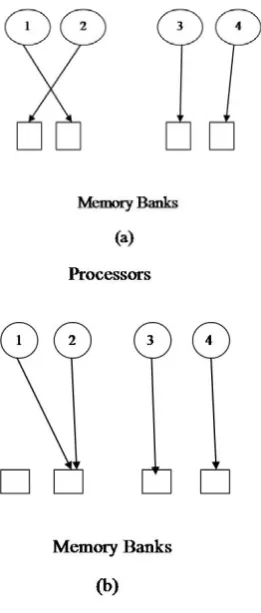
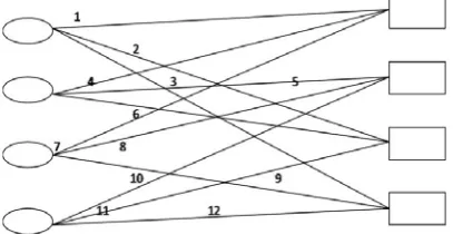
The first task is to decide which bit nodes will operate in parallel. The parity check matrix H, is represented as a Tanner Graph. This allows the edges to be numbered. The Tanner Graph is partitioned, placing the bit vertices into P sets, with an equal number of edges in each set, and check vertices into
Fig. 3. Number Tanner Graph
P sets, again with an equal number of edges in each set. The sets represent the group of bit nodes which are assigned to each bit processor. Experimental results have shown that graph partitioning can decrease the half 24 cycle iteration time, on average by 20% by reducing the number of potential memory collisions.
The second task is to graph edge variables to the memory banks. A mapping function is then generated, mapping the edges of the Tanner Graph to the memory banks is to avoid the memory collisions when each of the bit nodes acting in parallel access memory at the same time that shown in Fig 3.
The third and final task is to use the mapping function to determine the configuration required for the crossbar switches and the inter leaver banks. These tasks are discussed in detail in the following.
V. SIMULATION ANALYSIS
a.
Implementation of LDPC decoder to achieve high energy has been outlined by Simulation tool called ModelSim. It is a verification and simulation tool for VHDL, verilog, system verilog and mixed language designs. The lessons provides a brief conceptual overview of the ModelSim simulation environment.
A. Simulation Flow
In ModelSim, all designs are compiled into a library. You typically start a new simulation in ModelSim by creating a working library called “work”, which is the default library name used by the compiler as the default destination for compiled design units. After creating the working library, you compile your design units into it. The ModelSim library format is compatible across all supported platforms. You can simulate
your design on any platform without having to recompile your design. With the design compiled, you load the simulator with your design by invoking the simulator on a top-level module (Verilog) or configuration or entity/architecture pair(VHDL). Assuming the design loads successfully, the simulation is set to zero, and you enter a run command to begin simulation.
B. Analyzing Waveforms
The wave window allows you to view the results of your simulation as HDL waveforms and their values. The wave window is divided into a number of panes. You can resize the pathnames pane, the value pane and the window pane by clicking and dragging the bar between any two panes. Load the design , by starting the modelsim in UNIX shell prompt. After finish the design, add objects to the wave form. It has different methods, Add objects from the object window, Undock the Wave window, Adding objects using drag-and-drop also Adding objects using the add wave command.
C. Zooming the Waveform Display
The Wave window becomes a standalone, undocked window. Resize the window as needed. There are numerous methods for zooming the Waveform display. Zoom the display using various techniques, click the zoom mode on the icon on the window tool bar. In the wave form display, click and drag down to the right.
D. Simulation Results
The following figures describes schematically about the wave form and the respective outcomes from the simulation. Mapping of half adder and carry generator by using temp registers and the output of S will be generated according to output of carry generator“01111111” when “01” of c temp, “10000001” when “10”, of c temp. Output of mux will be based on the selection lines
VI. CONCLUSION
REFERENCES
[1] R. G. Gallager, “Low density parity check codes,” IRE Trans. Inf. Theory, vol. 8, no. , pp. 21–28, Jan. 1962.
[2] D. J. C. MacKay and R. M. Neal, “Near Shannon limit performance of low density parity check codes,” Electron. Lett., vol. 32, no. 18, pp. 1645–1646, 1996.
[3] The Digital Video Broadcasting Standard [Online]. Available: www.dvb.org.
[4] The IEEE P802.3an 10GBASE-T Task Force [Online]. Available: www.ieee802.org/3/an.
[5] The IEEE 802.16 Working Group [Online]. Available:
http://www.ieee802.org/16/.
[6] The IEEE 802.11n Working Group [Online]. Available:
http://www.ieee802.org/11/.
[7] J. Pearl, Probabilistic Reasoning in Intelligent Systems: Networks of
Plausible Inference. San Mateo, CA: Morgan Kaufmann, 1988.
[8] N. Wiberg, “Codes and Decoding on General Graphs,” Ph.D. dissertation, Electrical Engineering Dept., Linkoping Univ,, Linkoping, Sweden, 1996.
[9] F. Kschischang, B. Frey, and H. Loeliger, “Factor graphs and the sumproduct algorithm,” IEEE Trans. Inf. Theory, vol. 47, pp. 498–519, Feb. 2001.
[10] A.Tarrable, S.Benedetto , and G.Montorsi, “Mapping Interleaving laws to parallel turbo and LDPC decoder architectures” , IEEE Transactions on Information Theory , vol.50, no.9, pp 14-16, sept.2004.
[11] C.Shannon, “ A Mathematical theory of communication”, Bell System Technical Journal, vol.27 no.1 ,pp 379-423, 1948.
[12] S.Y.Chung, J.Forney, G.D., T.Richardson and R.Urbanke, “ On the design of low density parity check codes with 0.0045db of the Shannon limit”, Communications Letters, IEEE, vol.5 no.2, pp. 58-60, Feb 2011. [13] S.Johnson, “Introduction to Idpc codes “, in ACoRN Spring School on
Coding, Multiple User Communication and Random Theory, 2006. [14] Z. Zhang, V. Anantharam, M.J. Wainwright, and B. Nikolic,
“Anefficient 10GBASE-T ethernet LDPC decoder design with low errorfloors,” IEEE J. Solid-State Circ., vol.45, no.4, pp.843-855, Apr 2010.
[15] Saeed Sharifi Tehrani,Shie Mannor and Warren J. Gross, “Fully Parallel Stochastic LDPC Decoders”, IEEE TRANSACTIONS ON SIGNAL PROCESSING, VOL. 56, NO. 11, NOVEMBER 2008.
[16] H. Zhong and T. Zhang, “High-rate quasi-cyclic LDPC codes for magnetic recording channel with low error floor,” in Proc. of IEEE International Symposium on Circuits and Systems (ISCAS), May 2006, pp. 3546–3549.
[17] Saeed Sharifi Tehrani, Shie Mannor and Warren J. Gross, “An Area-Efficient Fpga-Based Architecture For Fully-Parallel Stochastic Ldpc Decoding” 1-4244-1222-6/07/$25.00 ©2007 IEEE.
[18] . Y. Chen and K. K. Parhi, “Overlapped message passing for quasi-cyclic low-density parity check codes,” IEEE Trans. Circuits Syst. I,