ISSN (Print) : 2320 – 3765 ISSN (Online): 2278 – 8875
I
nternational
J
ournal of
A
dvanced
R
esearch in
E
lectrical,
E
lectronics and
I
nstrumentation
E
ngineering
(An ISO 3297: 2007 Certified Organization)
Vol. 5, Issue 7, July 2016
Simulation Analysis for Voltage Sag
Mitigation Using Space Vector Pulse Width
Modulation Based DVR
S.D.Hire1, Prof.P.A.Desai2
PG Student, Dept. of Electrical Engineering, Matoshri College of Engineering, Nasik, Maharashtra, India1
Assistant Professor, Dept. of Electrical Engineering, Matoshri College of Engineering, Nasik, Maharashtra, India2
ABSTRACT: Most power quality problems in distribution systems are related to voltage sag. Therefore, different solutions have been examined to compensate these sags to avoid production losses at sensitive loads. Dynamic Voltage Restorer (DVR) have been proposed to provide higher power quality. In this paper, operation of DVR is presented along with the control technique used for voltage source inverter which is Space Vector Pulse Width Modulation (SVPWM).
KEYWORDS:Dynamic Voltage Restorer (DVR), Voltage Sag, Space Vector Pulse Width Modulation (SVPWM), Voltage Source Inverter (VSI).
I.INTRODUCTION
Power Quality problems consistof various disturbances such as voltage sags/swells, flicker, harmonics distortion, impulse transient, and interruptions [2]. Voltage sags can occur at any instant of time, with amplitudes ranging from 10 – 90% and a duration lasting for half a cycle to one minute [4]. Voltage swell is defined as an increase in rms voltage or current at the power frequency for durations from 0.5 cycles to 1 min. Typical magnitudes of swell are between 1.1 and 1.8 p.u. Voltage swells are not as important as voltage sags because they are less common in distribution systems. Voltage sag and swell can cause sensitive equipment (such as found in semiconductor or chemical plants) to fail, or shutdown, as well as create a large current imbalance that could blow fuses or trip breakers. Due to these effects both electric utilities and end users of electric power are concerned about quality of power. There are various methods to compensate voltage sags and swells, but the use of a custom Power device is considered to be the most efficient method[2].
In this paper, voltage sagis compensated using DVR (Dynamic Voltage Restorer) based on Space Vector Pulse Width Modulation (SVPWM) technique. MATLAB model based simulated results are presented to validate the effectiveness of the proposed control method of DVR.
II.DYNAMIC VOLTAGE RESTORER (DVR)
DVR is a series connected custom power device. Its main function is the protection of sensitive loads from any voltage disturbances except voltage outage [5], [6]. It basically consists of power circuit and control circuit. The power circuit of the DVR has four main parts: voltage source inverter (VSI), voltage injection transformer, DC energy storage device and low pass filter [6], [7] as shown in Figure 1.
ISSN (Print) : 2320 – 3765 ISSN (Online): 2278 – 8875
I
nternational
J
ournal of
A
dvanced
R
esearch in
E
lectrical,
E
lectronics and
I
nstrumentation
E
ngineering
(An ISO 3297: 2007 Certified Organization)
Vol. 5, Issue 7, July 2016
1.Voltage Injection/Booster Transformer:The basic function of injection transformer is to increase the voltage supplied by the filtered voltage source inverter (VSI) output to the desired level while isolating the DVR circuit from the distribution networks.
2.Harmonic Filter:Basically filter unit consists of inductor(L) and capacitor(C). In DVR, filters are used to convert the inverted PWM waveform into a sinusoidal waveform. This can be achieved by eliminating the unwanted harmonic components generated by the VSI actions.
3.Storage Devices:The DVR needs real power for compensation purposes during voltage disturbance in the distribution system. In this case the real power of the DVR must be supplied by energy storage when the voltage disturbance exits. The energy storage such as battery is responsible to supply an energy source in DC form.
4.DC Charging Circuit:The DC charging circuit has two main tasks; first task is to charge the energy source after a sag compensation event. And the second task is to maintain dc link voltage at the nominal dc link voltage.
III.PRINCIPLE OF SVPWM
The typical diagram of conventional three phase inverter consists of six thyristor devices and a DC voltage source with a constant load is as shown in Figure 2. SVPWM aims to generate a voltage vector that is close to the reference circle through the various switching modes of inverter.
Figure 2: Typical diagram of a three-phase inverter [11]
For the on-off state of the three-phase inverter circuit, every phase can be considered as a switch S. Here, SA(t), SB(t)
and SC(t) are used as the switching functions for the three phases, respectively. The space vector of output voltage of
inverter can be expressed as
V (SA, SB, SC) =2Vdc (SA+αSB+α2SC)/3……….... (1)
Where Vdc is the DC bus voltage of inverter and α=ej120. If we express the on state of the upper-arm with “1” and the off state with “0”, the on-off states of three phases have eight combinations, correspondingly forming eight voltage space vectors, as shown in Figure 4. T refers to the operation times of two adjacent non-zero voltage space vectors in the same zone. Both V0(000) and V7(111) are called the zero voltage space vector, and the other six vectors are called the effective
vector with a magnitude of 2Vdc/3. For example, when the output voltage vector V is within zone one, it is composed of
V4, V6, V0 and V7 and can be obtained by
Vout=TV4/T+TV6/T ………..(2)
ISSN (Print) : 2320 – 3765 ISSN (Online): 2278 – 8875
I
nternational
J
ournal of
A
dvanced
R
esearch in
E
lectrical,
E
lectronics and
I
nstrumentation
E
ngineering
(An ISO 3297: 2007 Certified Organization)
Vol. 5, Issue 7, July 2016
Table1:The eight on-off states of inverter
Inverter State SA SB SC SA SB SC VA/Vdc VB/Vdc VC/Vdc
0 000 111 0 0 0
1 001 110 -1/3 -1/3 2/3
2 010 101 -1/3 2/3 -1/3
3 011 100 -2/3 1/3 1/3
4 100 011 2/3 -1/3 -1/3
5 101 010 1/3 -2/3 1/3
6 110 001 1/3 1/3 -2/3
7 111 000 0 0 0
Figure 3: Diagram of Voltage Space Vector
IV.DYNAMIC VOLTAGE RESTORER WITH PI CONTROLLER
A controller is required to control or to operate DVR during the fault conditions only. Load voltage is sensed and passed through a sequence analyser. The magnitude of the actual voltage is compared with reference voltage (Vref).
Space Vector Pulse width modulated (SVPWM) control system is applied for inverter switching so as to generate a three phase 50 Hz sinusoidal voltage at the load terminals. Chopping frequency is in the range of a few KHz. The IGBT inverter is controlled with PI controller in order to maintain 1p.u. voltage at the load terminals. An advantage of a proportional plus integral controller is that its integral term causes the steady state error to be zero for a step input. PI controller input is an actuating signal which is the difference between the (Vref) and (Vin). Output of the controller block
is of the form of an angle, which introduces additional phase-lag/lead in the three-phase voltages. The output of error detector is (Vref) - (Vin) where (Vref) equal to 1 p.u. voltage and (Vin) voltage in p.u. at the load terminals, the controller
output when compared at PWM signal generator results in the desired firing sequence.
V.SIMULATION RESULT AND DISCUSSION
ISSN (Print) : 2320 – 3765 ISSN (Online): 2278 – 8875
I
nternational
J
ournal of
A
dvanced
R
esearch in
E
lectrical,
E
lectronics and
I
nstrumentation
E
ngineering
(An ISO 3297: 2007 Certified Organization)
Vol. 5, Issue 7, July 2016
Table 2: System Parameters and Constant Values [1]
Sr.No Equipment Ratings
1 Three phase Programmable Voltage Source 66000 V, 50 Hz
2 DC voltage source 100 V
3 Three phase three winding transformer
100MVA 50Hz, V1=66000V V2=11000V,
V3=11000V
4 Three phase two winding transformer V1=11000V V100MVA 50Hz, 2=415V
5 Injection transformer (12 terminals) V1=100V V10kVA 50Hz, 2=415V
6 Fault Time Logic T= 0.1-0.2sec, R=0.004 ohm
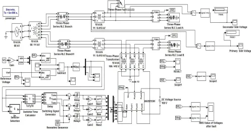
There are various components present in Simulink of distribution system; values of these various components are given in Table 2.Firstly, the main circuit was designed and implemented in the Matlab/Simulink.
Figure 5:Main System without DVR
ISSN (Print) : 2320 – 3765 ISSN (Online): 2278 – 8875
I
nternational
J
ournal of
A
dvanced
R
esearch in
E
lectrical,
E
lectronics and
I
nstrumentation
E
ngineering
(An ISO 3297: 2007 Certified Organization)
Vol. 5, Issue 7, July 2016
The Figure 6 shows the waveform of output voltage at feeder A and feeder B respectively, during LLLG fault. The fault occurred for duration of 0.1second to 0.2 second during which voltage at feeder A suddenly goes to zero and voltage at feeder B decreased than the nominal voltage i.e. phenomena voltage sag occurred on feeder B.
Figure 7: System connected with the Space Vector Pulse Width Modulation based DVR
The Figure 7 shows the complete distribution system with installation DVR during LLLG fault .The results obtained from the Simulink are discussed below.
Figure 8:Actual signal (sag) and reference signal respectively
ISSN (Print) : 2320 – 3765 ISSN (Online): 2278 – 8875
I
nternational
J
ournal of
A
dvanced
R
esearch in
E
lectrical,
E
lectronics and
I
nstrumentation
E
ngineering
(An ISO 3297: 2007 Certified Organization)
Vol. 5, Issue 7, July 2016
Figure 9:Actual signal and reference signal converted into dq0 form respectively
The figure 9 shows the actual and reference signal during voltage sag, which are to be converted into the dq0 transform frame.
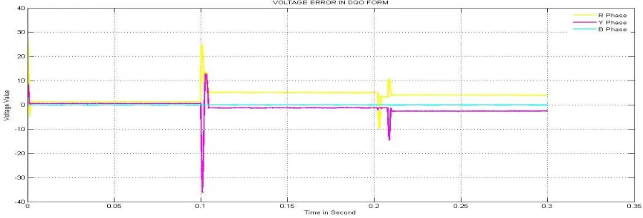
Fiqure 10:Voltage error signal dq0 transformation
The figure 10shows the voltage error between actual and reference signal during voltage sag.
Figure 11: Voltage error signal separated in d - q - 0 form
ISSN (Print) : 2320 – 3765 ISSN (Online): 2278 – 8875
I
nternational
J
ournal of
A
dvanced
R
esearch in
E
lectrical,
E
lectronics and
I
nstrumentation
E
ngineering
(An ISO 3297: 2007 Certified Organization)
Vol. 5, Issue 7, July 2016
Figure 12: Output from SVPWM
Figure 12 shows the output of the PWM in pulse form. The shape of waveform looks like solid. Actually, it is a pulse with magnitude one and zero repeatedly. Since the frequency used in the repeating square is very high.Therefore, it is hard tolook using naked eyes. Using high frequency will be resulted less losses and the result of the output of inverter in the end, is more accurate.
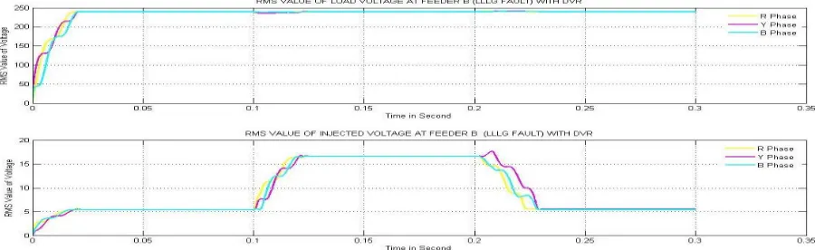
Figure 13: Output voltage and injected voltage at feeder B after compensation (with LLLG fault)
The figure13 shows the waveform of injected voltage at the feeder B which is added in the system to compensate the effect of voltage sag which is occuried due to three line to ground fault at distribution system.
ISSN (Print) : 2320 – 3765 ISSN (Online): 2278 – 8875
I
nternational
J
ournal of
A
dvanced
R
esearch in
E
lectrical,
E
lectronics and
I
nstrumentation
E
ngineering
(An ISO 3297: 2007 Certified Organization)
Vol. 5, Issue 7, July 2016
The figure 14. shows the RMS value of injected voltage at the feeder B which is added in the system to compensate the effect of voltage sag which is occuried due to three line to ground fault at distribution system.
VI.CONCLUSION
This work describes one of the methods to mitigate the voltage sag by using dynamic voltage restorer system. In order to investigate whether the DVR is able to deal with this problem, Matlab/Simulink based approach is selected in order to simulate the system and mitigate the voltage sag. Based on the simulation, it can be proved that DVR is the dynamic fast response devices which is able to overcome the devices.
Even though the system cannot compensate 100 percent of voltage during sag always, it is an acceptable value because the output voltage after compensation still in range of the nominal value. Since DVR is the custom power devices, there are so various combinations of main component that can be combined in order to get better results. For example, using GTO as a switching device, using SVPWM as the device for generating gating signal or maybe can use the other type of filter in order to eliminate the harmonics. The design of DVR can be improved by adding a PI controller while designing DVR. Thus, it can control the circuit with more accuracy and improve the response of the DVR. SVPWM based technique is able to generate an output voltage with minimum of harmonic and distortion.
REFERENCES
[1] Changjiang Zhan, V. K. Ramachandramurthy, and C. Filtzer, “Dynamic Voltage Restorer Based on Voltage Space Vector PWM Control,” IEEE Transactions on Industry Applications, vol. 37, no. 2, pp. 1855-1863, 2012.
[2] N.G.Hingorani,“Intoducing Custom Power in IEEE Spectrum,”32p, pp. 41-48,1995.
[3] IEEE Recommended Practice for Monitoring Electric Power Quality," in IEEE Std 1159-1995 , vol., no., pp.i-, 1995. [4] A.Ghosh and G.Ledwich,“Power Quality Enhancement Using Custom Power Devices,”Kluwer Academic Publisher,2002.
[5] Shairul Wizmar Wahab and Alias Mohd Yusof, “Voltage Sag and Mitigation Using Dynamic Voltage Restorer (DVR) System”,electrika, vol.8, No.2, pp. 32-37, 2006.
[6] L. Sarıbulut, Performance analysis of unified power flow controller(UPFC) by using different controllers, M.Sc. thesis, Department of
Electrical and Electronic Engineering, Cukurova University, 2008..
[7] R. Mihalic, P. Zunko and D. Povh, "Improvement of transient stability using unified power flow controller," in IEEE Transactions on Power Delivery, vol. 11, no. 1, pp. 485-492, Jan 1996.
[8] "Proposed terms and definitions for flexible AC transmission system (FACTS)," in IEEE Transactions on Power Delivery, vol. 12, no. 4, pp. 1848-1853, Oct 1997.
[9] Hernandez, K.E. Chong, G. Gallegos, and E. Acha, “Theimplementation of a solid state voltage source in PSCAD/EMTDC,” IEEE Power Eng. Rev., pp. 61-62, dec. 1998.
[10] P. Flores, J. Dixon, M. Ortuzar, R. Carmi, P. Barriuso, and L.Moran, “Static Var compensator and active power filter with power injection capability, using 27-level inverters and photovoltaic cells,” IEEE Trans. Ind. Electron., vol. 56, no. 1, pp.130–138,Jan.2009.
[11] B. Vladimir and K. Vikram, “A new mathematical model and control of a three-phase AC–DC voltage source converter,” IEEE Transactions on Power Electronics, vol. 12, no. 1, pp. 116-123, 1997.
[12] R. Wu, S. B. Dewan, and G. R. Slemon, “A PWM AC to DC converter with fixed switching frequency,” IEEE Trans. on Industry Applications, vol. 26, no. 5, pp. 880-885, 1990.

![Figure 2: Typical diagram of a three-phase inverter [11]](https://thumb-us.123doks.com/thumbv2/123dok_us/7775372.1281974/2.595.162.425.373.519/figure-typical-diagram-phase-inverter.webp)
![Table 2: System Parameters and Constant Values [1]](https://thumb-us.123doks.com/thumbv2/123dok_us/7775372.1281974/4.595.87.539.602.767/table-system-parameters-and-constant-values.webp)