ISSN (Print) : 2320 – 3765 ISSN (Online): 2278 – 8875
I
nternational
J
ournal of
A
dvanced
R
esearch in
E
lectrical,
E
lectronics and
I
nstrumentation
E
ngineering
(A High Impact Factor, Monthly, Peer Reviewed Journal)
Website: www.ijareeie.com Vol. 8, Issue 11, November 2019
Design and Implement Low Power in Different
type of Adders
Ankur Sharama, Abha Sharma
Research Scholar M.Tech. VLSI, RIET, Jaipur, India Assistant Professor, RIET, Jaipur, India
ABSTRACT: In this paper 1-bit adder has been designed and simulated using 180 nm CMOS technology in tanner tool at a various supply voltage from 1.0V to 1.8 V & compare their results with respect to various parameters like delay, area & power consumption. The adder is the most commonly used arithmetic block of the Central Processing Unit (CPU) and Digital Signal Processing (DSP), therefore its performance and power optimization is of utmost importance. With the technology scaling to deep sub-micron, the speed of the circuit increases rapidly.
Due to continuous scaling of the transistor size and reduction of the operating voltage has led to a significant performance improvement of integrated circuits. Low power consumption and smaller area are some of the most important criteria for the fabrication of DSP systems and high performance systems. At the same time, the power consumption per chip also increases significantly due to the increasing density of the chip.
I. INTRODUCTION
Rapid growth in semiconductor technology has led to shrinking of feature sizes of transistors using deep submicron (DSM) process. Modern portable battery operated devices such as cell phones, laptops; PDAs are particularly affected by this as high power dissipation reduces battery service life. The adder is the most commonly used arithmetic block of the Central Processing Unit (CPU) and Digital Signal Processing (DSP), therefore its performance and power optimization is of utmost importance. With the technology scaling to deep sub-micron, the speed of the circuit increases rapidly. At the same time, the power consumption per chip also increases significantly due to the increasing density of the chip. Therefore, in realizing modern Very Large Scale Integration (VLSI) circuits, low-power and high-speed are the two predominant factors which need to be considered. Like any other circuits' design, the design of high-performance and low-power adders can be addressed at different levels, such as architecture, logic style, layout, and the process technology. As the result, there always exists a trade-off between the design parameters such as speed, power consumption, and area. Recently, the requirement of probability and the moderate improvement in battery performance indicate power dissipation is one of the most critical design parameters day by day the demand of probability and mobility is increasing.
Adders are commonly used in the critical path of many building blocks of microprocessors and digital signal processing chips. Adders are critical component not only for addition, but also for subtraction, multiplication, and division. Addition is one of the fundamental arithmetic operations. A fast and accurate operation of a digital system is greatly influenced by the performance of the resident adders. The most important parameter for measuring the quality of adder designs is propagation delay, and area.
ISSN (Print) : 2320 – 3765 ISSN (Online): 2278 – 8875
I
nternational
J
ournal of
A
dvanced
R
esearch in
E
lectrical,
E
lectronics and
I
nstrumentation
E
ngineering
(A High Impact Factor, Monthly, Peer Reviewed Journal)
Website: www.ijareeie.com Vol. 8, Issue 11, November 2019
II. APPLICATION OF ADDERS
Used in CPU side
Used in networking side
Used in DSP oriented system
In application-specific processors
In biomedical applications
In image processing and video processing.
Types of Adder
For single bit adders, there are two general types of adders which are given below
1. Half Adder
2. Full Adder
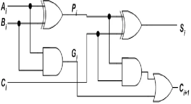
Carry Look Ahead Adder circuit
A carry-look ahead adder (CLA) is a type of adder used in digital logic that improves speed by reducing the amount of
computation time required to determine carry bits. It works by creating two signals P and G known as Carry Propagator
signal and Carry Generator signal. The carry propagator signal is propagated to the next level whereas the carry generator is used to generate the output carry, regardless of input carry. Carry signal will be generated in two cases:
1. When both bits A
i and Bi are 1, or
2. When one of the two bits is 1 and the carry-in (carry of the previous stage) is 1.
ISSN (Print) : 2320 – 3765 ISSN (Online): 2278 – 8875
I
nternational
J
ournal of
A
dvanced
R
esearch in
E
lectrical,
E
lectronics and
I
nstrumentation
E
ngineering
(A High Impact Factor, Monthly, Peer Reviewed Journal)
Website: www.ijareeie.com Vol. 8, Issue 11, November 2019
i i
i
A
B
G
The output sum and carry can be defined as:
i i
i
P
C
S
i i i
i
G
P
C
C
1
G
i is known as the carry Generate signal since a carry (Ci+1) is generated whenever Gi =1, regardless of the input carry
(C
i).
P
i is known as the carry propagate signal since whenever Pi =1, the input carry is propagated to the output carry, i.e.
i
i
C
C
1
(Whenever Pi =1, Gi =0)The Boolean expression of the carry outputs of various stages can be written as follows: C
1 = G0 + P0C0
C
2 = G1 + P1C1 = G1 + P1 (G0 + P0C0) = G1 + P1G0 + P1P0C0
C
3 = G2 + P2C2 = G2 + P2G1 + P2P1G0 + P2P1P0C0
C
4 = G3 + P3C3 = G3 + P3G2 + P3P2G1 + P3P2P1G0 + P3P2P1P0C0
The disadvantage of the CLA adders is that the carry expressions (and hence logic) become quite complex for more than 4 bits.
FULL ADDER TOPOLOGY
In microprocessor and DSP`s, addition is the most commonly used arithmetic operation and it is often one of the speed-limiting elements. Hence optimization of the adder both in terms of speed and/or power consumption should be pursued. During the design of an adder two choices are made in regard to different design abstraction levels. One is responsible for the adder’s architecture implemented with the one-bit full adder as a building block. The other defines the specific design style at transistor level to implement the one-bit full adder.
DGTAL ADDER
ISSN (Print) : 2320 – 3765 ISSN (Online): 2278 – 8875
I
nternational
J
ournal of
A
dvanced
R
esearch in
E
lectrical,
E
lectronics and
I
nstrumentation
E
ngineering
(A High Impact Factor, Monthly, Peer Reviewed Journal)
Website: www.ijareeie.com Vol. 8, Issue 11, November 2019
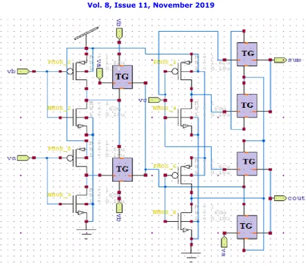
Fig 2: Circuit Diagram of DGTAL Adder DGTAL ADDER
20 transistor full adder based on transmission gate produces buffered outputs of proper polarity for both sum and carry. In this circuit 2 inverters are followed by two transmission gates which act as 8-T XOR. Subsequently 8-T XNOR module follows. To has 4 transistors XOR which in the next stage is inverted to produce XNOR. These XOR and
XNOR are used generate sum; C in and
C
inare multiplexed which can simultaneously to generate sum. The signals cin is controlled either by (a. b) or (a ⊗b). Similarly the c out can be calculated by multiplexing a and cincontrolled by
ISSN (Print) : 2320 – 3765 ISSN (Online): 2278 – 8875
I
nternational
J
ournal of
A
dvanced
R
esearch in
E
lectrical,
E
lectronics and
I
nstrumentation
E
ngineering
(A High Impact Factor, Monthly, Peer Reviewed Journal)
Website: www.ijareeie.com Vol. 8, Issue 11, November 2019
Fig 3: Schematic Diagram of DGTAL Adder III. SIMULATION RESULTS
DGTAL ADDER
Working principle: In the circuit we have 2 inverters followed by two transmission gates which act as 8-T XOR. Subsequently8-T XNOR module follows. To generate sum, c in and c in b are multiplexed which can controlled either
by (a b) or (a ⊗b).Similarly the c out can be calculated by multiplexing a and c in which is controlled by (a b).
ISSN (Print) : 2320 – 3765 ISSN (Online): 2278 – 8875
I
nternational
J
ournal of
A
dvanced
R
esearch in
E
lectrical,
E
lectronics and
I
nstrumentation
E
ngineering
(A High Impact Factor, Monthly, Peer Reviewed Journal)
Website: www.ijareeie.com Vol. 8, Issue 11, November 2019
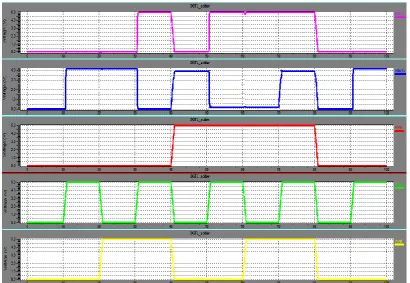
Fig 3: Simulated waveform of DGTAL Adder Advantage: It is the fastest adder.
The circuit is simpler than the conventional adder.
Disadvantage: The power dissipation in this circuit is more than the 28T adder.
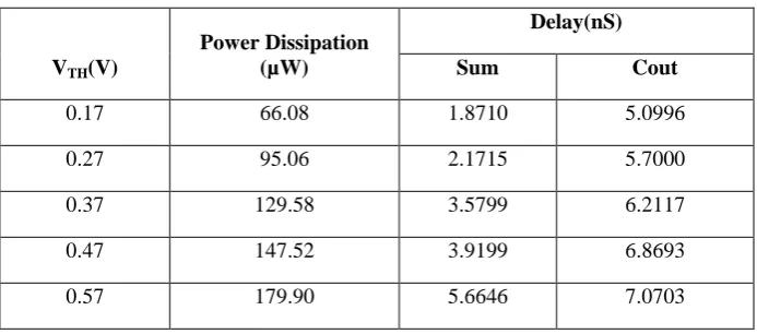
Parameters like delay and power dissipation is calculated at different VDD and at different VTH, which is shown in table
1 and 2 respectively.
Table 2: Parameters of DGTAL adder at different VDD
VDD(V)
Power Dissipation (µW)
Delay(nS)
Sum Cout
1.8 129.585 4.040 5.211
ISSN (Print) : 2320 – 3765 ISSN (Online): 2278 – 8875
I
nternational
J
ournal of
A
dvanced
R
esearch in
E
lectrical,
E
lectronics and
I
nstrumentation
E
ngineering
(A High Impact Factor, Monthly, Peer Reviewed Journal)
Website: www.ijareeie.com Vol. 8, Issue 11, November 2019
Table 2: Parameters of DGTAL adder at different VTH
VTH(V)
Power Dissipation (µW)
Delay(nS)
Sum Cout
0.17 66.08 1.8710 5.0996
0.27 95.06 2.1715 5.7000
0.37 129.58 3.5799 6.2117
0.47 147.52 3.9199 6.8693
0.57 179.90 5.6646 7.0703
IV. CONCLUSION
In this paper adder has been designed and simulated using 180 nm CMOS technology of tanner tool at a various supply voltage from 1.0V to 1.8 V& compare their results with respect to various parameter. The comparison has been carried out both assuming circuits with minimum transistors size, to minimize the power consumption. Power consumption is a function of load capacitance, frequency of operation, and supply voltage. A reduction of any one of these is beneficial. A reduction in power consumption provides several benefits. Less heat is generated, which reduces problems associated with high temperature, such as the need for heat sinks. This provides the consumer with a product that costs less. In this paper we conclude that
REFERENCES
[1] N. Firake and S. Akashe, “Power-Delay Product Minimization of Mixed Full Adder Topologies for High-Performance”, African Journal
of Computing & ICT, Vol 7. No. 2, pp: 93-98, ISSN 2006-1781, June, 2014.
[2] Ruchika Sharma and Rajesh Mehra, “Design of Error-Tolerant CMOS Adder Usingoptimized Transistor Count”, International Journal of
Advanced Research in Computer and Communication Engineering, Vol. 3, Issue 7, ISSN (Print) : 2319-5940, July 2014.
[3] BaminGambo, Lod Tapin and Sarat Chandra Hanjabam, “ Low Power and High Performance Full Adder in Deep Submicron
Technology”, Journal of Electronics and Communication Engineering Research Volume 2, Issue 3 pp: 07-16 ISSN : 2321-594, 2014
[4] Namarta and Mr. Sukhjit Singh, “ Comparative Analysis Different Adder Topologies using 180 nm Technology”, International Journal
for Science and Emerging Technologies with Latest Trends, Volume 14, Issue 1 pp: 07-11,ISSN No. : 2277-8136, 2014.
[5] S. Arif Basha & C. V. Subhaskara Reddy, “Low Power Highly Optimized Full Adder By Using Different Techniques With 10
Transistors”, International Journal of Engineering Research, Volume No. 3 Issue No: Special 2, pp: 95-96, ISSN:2319-6890, 22 March 2014.
[6] K Srinivas Raju and Dr. B. R. Vikram, “Competent Fetch Select Adder using 0.12 μm Expertise for Low Power Applications”,
International Journal of Research in Modern Engineering and Emerging Technology, Vol. 2, Issue: 2, pp: 16-22,ISSN: 2320-6586, June-July 2014.
[7] Kandimalla Brahmani and Danda Aneesha, “Analysis of Full Adder Design using Various CMOS Design”, International Journal of
Engineering & Science Research, Vol-4, Issue-7, pp:409-414, ISSN 2277-2685, July 2014.
[8] T. S. Ananth, A. Vijay and Dr. G.K.D. Prasanna Venkatesan, “Low-Power 1-Bit Full-Adder Cell using Enhanced Pass Transistor Logic
and Power Gating”, International Journal of Advanced Technology in Engineering and Volume No. 02, Issue No. 06,pp:1-8 ISSN: 2348 – 7550 ,June 2014.
[9] V. Narayana Reddy and G. Sai Sindhu, “Design of Low Power 4 bit Ripple Carry Adder using DPTA synchronous Adiabatic Logic”,
International Journal of Computational Science, Mathematics and Engineering, Volume 1, Issue 5, pp: 50-59, ISSN: 2349-8439, November 2014.
[10] Tran Bich Thuan Pham, Yi Wang and Renfa Li, “Designing one-bit Full-Adder/Subtractor based on Multiplexer and LUT’ sarchitecture
on FPGA”, International Journal of Digital Content Technology and its Applications, Volume 7, Number 8, issue 8, pp: 454-464, April 2013.
[11] C. Channe Gowda and Dr. A.R. Aswatha, “Low-Power 1-Bit Full-Adder Cell Using Modified Pass Transistor Logic”, International