University of Twente
Faculty of Electrical Engineering,
Mathematics & Computer Science
Low-power
analog-to-digital conversion
Michiel van Elzakker MSc. Thesis December 2006
Supervisors: ir. P.F.J. Geraedts prof. ir. A.J.M. van Tuijl ir. D. Schinkel dr. ing. E.A.M. Klumperink
Report number: 006.3189 Chair of Integrated Circuit Design Faculty of Electrical Engineering, Mathematics & Computer Science
1 Abstract
The subject of this graduation project is low-power analog-to-digital conversion. A motivation for the subject is that power consumption is a critical criterion for some ADC applications. The first project goal is the investigation of low-power ADC architectures and building blocks on the conceptual and circuit level. The second project goal is the development of a chip to test and demonstrate some of these circuits.
Limitations on low-power analog-to-digital conversion are explored. It is concluded that the figure of merit, a widely accepted benchmark for low-power analog-to-digital conversion, does not correspond to fundamental limitations. It is also concluded that it depends on the number of bits how easy it is to reach a certain FOM.
The scope of an ADC is explored. Various conceptions exist about when a circuit deserves to be called ADC. A set of conditions is selected.
Various ADC architectures are qualitatively compared on their suitability for low-power analog-to-digital conversion. It is concluded that logarithmic approximation is the most suitable one for low-power analog-to-digital conversion. One such architecture is selected for development, the
successive approximation architecture.
Building blocks for low-power analog-to-digital conversion are explored. These include techniques to dissipate less total comparator energy regardless of the comparator architecture. Level creation based on charge redistribution is explored and it is concluded that there is no fundamental lower limit on energy dissipation of digital-to-analog conversion. Also a new comparator architecture is developed that is efficient in terms of noise per energy.
Table of Contents
1 Abstract...3
2 Introduction... 7
3 Limitations on low-power analog-to-digital conversion... 9
3.1 Signals and their electrical representation... 9
3.1.1 Signals ...9
3.1.2 Electrical quantities...9
3.1.3 Mapping of signals onto electrical quantities... 9
3.1.4 Working with signals... 9
3.2 Analog and amplitude-continuous time-discrete signal processing... 9
3.2.1 Amplitude-continuous time-discrete signals...10
3.2.2 Technology limitations... 10
3.2.3 Noise... 10
3.2.4 Power, energy and signal to noise ratio... 11
3.2.5 Impedance scaling...12
3.3 Digital signal processing...12
3.4 Information and signal processing...12
3.4.1 Fixed amount of information and information rate...12
3.4.2 Maximum amount of information...12
3.4.3 Energy and amount of information - Shannon...13
3.4.4 Energy and amount of information - time-discrete... 13
3.4.5 Energy and amount of information - digital...14
3.4.6 Energy and amount of information - comparison... 14
3.5 Analog-to-digital conversion... 14
3.5.1 SNR and number of bits...14
3.5.2 Effective number of bits and figure of merit...14
3.5.3 Comparison of FOM with limitations...15
4 Scope of an ADC...17
4.1 Essential functions... 17
4.1.1 Amplitude discretization and digital output...17
4.1.2 Time discretization...17
4.2 Minimum specifications... 17
4.2.1 Accuracy... 17
4.2.2 Input... 17
4.2.3 Output...18
4.2.4 Conversion speed... 18
4.3 References requirements...18
4.3.1 Voltage and current references... 18
4.3.2 Time or frequency references... 18
5 Low-power ADC implementation...19
5.1 Overview of ADC architectures... 19
5.1.1 Direct conversion... 19
5.1.2 Linear approximation... 19
5.1.3 Logarithmic approximation...19
5.1.4 Selection of architectures... 19
5.2 Sample-and-hold circuitry... 20
5.3 Level creation... 20
5.4 Comparison...21
5.4.2 Effects of comparison imperfections... 21
5.4.3 Comparison power dissipation...21
5.5 Digital circuitry...22
5.6 Comparison of architectures... 23
6 Low-power successive approximation ADC...25
6.1 Basic principle... 25
6.2 Comparison energy reduction...25
6.2.1 Over-range... 25
6.2.2 Smaller average number of comparisons... 26
6.2.3 Over-sampling...27
6.2.4 Over-sampling with feedback... 27
6.3 Charge redistribution level creation for SAR... 27
6.3.1 Two-capacitor architecture... 28
6.3.2 Traditional weighted-capacitor architecture... 28
6.3.3 Alternative weighted-capacitor architecture... 29
6.3.4 Accuracy through settling... 29
6.3.5 Dissipation during charging and discharging of capacitors... 30
6.3.6 Reduction of dissipation...30
6.3.7 Thermal noise lower limit on capacitor value...32
6.3.8 Matching lower limit on capacitor value... 32
6.3.9 Comparison of lower limits...34
6.4 Comparator... 34
6.4.1 Architectures... 34
6.4.2 New comparator topology...35
6.4.3 Operation and gain calculations... 35
6.4.4 Noise calculations... 36
6.4.5 Noise simulations... 37
6.4.6 Theoretical further energy reduction...38
7 Development of test and demonstration chip... 39
7.1 Goals... 39
7.1.1 Demonstration... 39
7.1.2 Test...39
7.2 Design... 39
7.2.1 Process... 39
7.2.2 Design for testability... 40
7.2.3 Number of bits... 40
7.2.4 Basic architecture and main additional techniques... 40
7.2.5 References... 40
7.2.6 Delay line implementation... 40
7.2.7 Capacitor value and converter range...41
7.2.8 Application of DC/DC conversion techniques...41
7.2.9 Comparator implementation... 41
7.2.10 Bootstrapped differential sample-and-hold...42
7.3 Post layout simulation results... 42
7.4 Future work...42
8 Conclusions and recommendations for future work...43
2 Introduction
An analog-to-digital converter (ADC) is one of the most common building blocks of modern integrated circuits. Many different designs are in use today to meet a very wide range of requirements. For some applications the power consumption of the ADC is a critical criterion. The subject of this graduation project is low-power analog-to-digital conversion. The first project goal is the investigation of low-power ADC architectures and building blocks on the conceptual and circuit level. The second project goal is the development of a chip to test and demonstrate some of these circuits.
Chapter 3 explores limitations on low-power analog-to-digital conversion. Because an ADC is a signal processing building block signals are discussed first. Next signal processing and limitations on signal processing are discussed. These limitations include technology limitations and noise. The purpose of a signal is conveying information. Properties of information are discussed next. Finally chapter 3 discusses some properties of analog-to-digital conversion. A figure of merit is discussed and compared to signal processing limitations.
Chapter 4 explores the scope of an ADC. Especially when developing a low-power ADC it is necessary to consider when a circuit can reasonably be called an ADC.
Various ADC architectures exist. In chapter 5 they are qualitatively compared on their suitability for low-power analog-to-digital conversion. A conclusion is drawn after considering the same aspects for every architecture.
In chapter 6 building blocks for low-power analog-to-digital conversion are explored. They are mainly geared towards logarithmic approximation with the main emphasis on successive
approximation. First techniques are discussed to dissipate less total comparator energy regardless of the comparator architecture. Next level creation based on charge redistribution is discussed. After that work on a new comparator architecture is discussed.
Chapter 7 discusses the development of the test and demonstration chip. A 65nm process is used. Its specifications are chosen such that they are favorable for a low figure of merit.
3 Limitations on low-power analog-to-digital conversion
An ADC is a signal processing circuit. This chapter discusses some background on signalprocessing and various limitations. The reader should feel free to initially skip any part that seems familiar.
3.1 Signals and their electrical representation
This paragraph first discusses signals. Then electrical quantities are discussed. Next it is discussed how signals can be mapped onto electrical quantities. Finally working with signals is discussed.
3.1.1 Signals
A signal is something that can be used to convey information. It can be discrete or continuous in time and amplitude. An analog signal is continuous in both time and amplitude. A digital signal is discrete in both time and amplitude.
3.1.2 Electrical quantities
In an integrated circuit electrical quantities can be used to represent signals. The fundamental electrical quantities are charge and flux, which are manifested as voltages on capacitances and currents through inductors. Electrical quantities are usually considered to be time and amplitude continuous in nature.
3.1.3 Mapping of signals onto electrical quantities
An analog signal can straightforwardly be mapped onto an electrical quantity, because both are continuous. It is less straightforward to represent digital signals by electrical quantities. It is common practice to represent a bit by a node voltage. A digital one can be a voltage close to the positive supply voltage and a digital zero a voltage close to the negative supply voltage.
3.1.4 Working with signals
When considering an integrated circuit it is not feasible to take all known fundamental quantities and effects into account. Simplification is necessary in order to work with signals. The
simplification an analog developer usually uses is to consider voltages as the main carrier of signals. A circuit simulator has a numerical processing power that is superior to that of an analog developer. As a result less simplification is required and more state variables than just voltages can be taken into account. State variables can include for example charge, current and temperature. In principle a circuit simulator is just as suitable for an ADC with a voltage input as for an ADC with a different input. In a practical simulation environment not all state variables are available outputs by default.
3.2 Analog and amplitude-continuous time-discrete signal processing
3.2.1 Amplitude-continuous time-discrete signals
Amplitude-continuous time-discrete signals can arise from sampling analog signals. Sampling is often a first step in analog-to-digital conversion. Sampling is also required for switched capacitor filters. These filters can have implementation advantages over continuous-time filters.
The electrical quantities used to represent time-discrete signals can not truly be time-discrete. When, for example, a voltage has been sampled onto a capacitor there are still mechanisms causing deviations in the charge. These mechanisms can include current through an off resistance of a switch or electron tunneling through a MOST gate.
3.2.2 Technology limitations
In a bulk process, devices are manufactured with limited accuracy. As a results there are unknown lattice defects and there is uncertainty in doping and device dimensions. For a circuit designer the limited accuracy is manifested by device parameter variation, flicker noise and a minimum allowed feature size. Some fundamental limitation for these factors exists. So far, a newer and better
controlled technology can give better results.
Device parameter variation is stochastic with a high correlation between devices on the same integrated circuit. Flicker noise is stochastic with a high correlation in time. The results of both effects on system behavior depends on design.
For hand calculations first-order models exist for the stochastic mismatch between components. Examples are the threshold voltage mismatch between equally designed transistors (1) and the capacitance mismatch between equally designed capacitors (2). A design manual can contain these matching parameters in some form. Compact models for simulation can contain a more complex model.
VT=
AVT
W⋅L[V] (1)C=AC⋅
C[F] ⇔C
C= AC
C⋅100[%] (2)With careful layout a very large range of capacitor values obeying formula (2) can be made available. A process provider can specify a predefined capacitor layout for a limited capacitance range. The parameter ACand minimum and maximum values for the capacitance are guaranteed. Custom layout is required when the provided capacitance range is insufficient for a purpose. The parameter ACand minimum and maximum values can not be obtained from the design manual.
3.2.3 Noise
Thermal noise and shot noise result in relevant fundamental limitations for signal processing. Both are modeled by a Gaussian distribution with zero mean. In the time-domain they can be
characterized by a standard deviation in an electrical quantity. Frequency-domain equivalents exist. Depending on the application noise can be regarded as time-continuous or time-discrete.
v=
4⋅k⋅T⋅R⋅B[V] ⇔ i=
4⋅k⋅TR ⋅B[A] (3)
v=
⋅ 4⋅k⋅Tgm ⋅B≈
4⋅k⋅T
gm ⋅B[V] (4)
v=
2⋅q⋅IDS⋅B⋅ 1gm[V] (5) IDS
gm≈m⋅Vth=
m⋅k⋅T
q [V] (6)
v=
2⋅q⋅IDS⋅B⋅ 1gm=
2⋅q⋅ m⋅k⋅Tq ⋅
1
gm⋅B=
2⋅m⋅k⋅T gm ⋅B≈
4⋅k⋅T
gm ⋅B[V] (7)
A time-discrete voltage signal can be obtained by sampling a time-continuous voltage signal onto a capacitor. The corresponding noise voltage is time-discrete as well. Its magnitude depends on the capacitance and is given in formula (8). The formula is valid after the transitional sampling effects and assumes sampling through a resistor with temperatureT.
v=
k⋅T
C [V] (8)
3.2.4 Power, energy and signal to noise ratio
Sometimes an electrical quantity can be associated with a resistor, capacitor or inductor. A corresponding power (9) or energy (10) can be calculated from magnitude. Formula (9) describes the power dissipated in a resistor. It can especially be useful for power calculations on time-continuous signal processing.
Formula (10) describes energy that is stored. It can especially be useful for power calculations on time-discrete signal processing. Capacitors in corresponding circuits are charged and discharged every cycle. During charging and discharging the stored energy is generally dissipated. Power dissipation is the product of the energy dissipation during one cycle and the cycle rate (11).
P=V2
R [W] ⇔ P=I
2
⋅R[W] (9)
E=1 2⋅C⋅V
2
[J] ; E=1 2⋅L⋅I
2
[J] (10)
P=E⋅f[W] (11)
SNR=Psignal
Pnoise
=V2/R V
2
/R= V2
V
2 [ ] ; SNR=
Psignal Pnoise
=I2⋅R I
2
⋅R= I2
I
2[ ] (12)
For time-continuous signals the noise magnitude depends on the bandwidth. Formula (13) is a general expression where N0is the power spectral density.
SNR=NP
0⋅B
[] (13)
3.2.5 Impedance scaling
It is generally possible to adapt the noise performance of a given circuit topology with little development effort. Every impedance and transconductance needs to be scaled by the same factor. This scales power consumption (9) and signal-to-noise ratio (12) by that factor. Noise variance is scaled by that same factor while noise magnitude (3) is scaled by the square root of the factor. The mechanism is called impedance scaling.
3.3 Digital signal processing
Digital signals suffer from the same noise and technology limitations as analog and amplitude-continuous time-discrete signals. However, in current processes their integrity is generally not affected by them. There are two reasons for this.
First, there are minimum feature sizes that result in relatively large parasitic capacitance at all digital signal nodes. The error voltage (9) will be orders of magnitude smaller than the signal range, resulting in a negligible chance of misinterpretation. Second, in typical digital circuits the signals are regenerated at every node.
3.4 Information and signal processing
The purpose of signal processing is handling the corresponding information. Amounts of
information and their relation with energy is discussed. This is done in order to be able to consider the efficiency of an ADC related to energy and amount of information.
3.4.1 Fixed amount of information and information rate
Signals can consist of discrete symbols or some continuous quantity. A set of discrete symbols can represent a fixed amount of information N[bits]. When there is not such a set it can be more practical to define an information rate. An information rate RHcan be defined as the product of the amount of information and the cycle rate (14).
RH=N⋅f[bits/s] (14)
3.4.2 Maximum amount of information
Nmax=log2sl=l⋅log2s[bits] (15)
In theory an amplitude continuous quantity has an infinite number of possible values. That would make the amount of information that could be represented infinite as well. In nature there is always a mechanism limiting the number of distinguishable values. An electrical quantity is accompanied by a Gaussian noise component. As a result the amount of information that can be represented by an instantaneous electrical quantity depends on the desired certainty.
Shannon defined the channel capacityC. If the information rateRHis lower than the channel capacity a theoretical coding exists such that any desired certainty can be achieved (16). Shannon derived (17) for a communication channel with additive white Gaussian noise.
RHC[bits/s] (16)
C=B⋅log21SNR[bits/s] (17)
3.4.3 Energy and amount of information - Shannon
For a large SNR Shannon's formula for channel capacity can be approximated by (18). Using formula (13) gives (19). It is now stated thatRHis proportional toC(20), which is approximately true for a constant modulation. Formula (21) results by inserting formulas (11), (14) and (20) into (19). It is the energy of a symbol with information N. The energy per bit is proportional to (22).
C SNR≈≫1B⋅log2SNR[bits/s] (18)
P∝B⋅2C/B[W] (19)
RH∝C[bits/s] (20)
E∝B
f⋅2
N⋅f/B
[J] (21)
E∝NB ⋅f⋅2
N⋅f/B =RB
H
⋅2RH/B[J]
(22)
Shannon also derived from formula (17) that the highest ratio between channel capacity and power is obtained for a very low SNR. Formula (23) is a first order Taylor approximation valid for a small SNR. Combining (23) and (13) yields (24). Formula (25) results by inserting formulas (11), (14) and (20) into (24). The energy per bit does not depend on the number of bits.
CSNR≈≪1B⋅SNR
ln2 [bits/s] (23)
C≈ P
N0⋅ln2[bits/s] (24)
E∝N[J] (25)
3.4.4 Energy and amount of information - time-discrete
factor of two. It yields one extra bit of information (15). Impedance scaling tells that the energy is quadrupled. This reasoning results in (26). The actual proportionality constant depends on the desired certainty.
E∝4N
[J] (26)
3.4.5 Energy and amount of information - digital
For simple digital signal processing the amount of energy required is a linear function of the amount of information. This is because both energy and information processed scale linearly with both operating frequency and number of parallel processing units.
3.4.6 Energy and amount of information - comparison
Formulas (21) and (26) are for amplitude-continuous processing with a high SNR. Energy is an exponential function of the amount of information. For analog signal processing with a low SNR the relation is more favorable and linear (25). For digital signal processing the relation is linear as well. As a result high precision signal processing generally requires less energy in the digital domain.
3.5 Analog-to-digital conversion
First the relation between the number of bits and signal-to-noise ratio is discussed. It is generalized to the relation between effective number of bits and signal-to-noise-and-distortion. A widely accepted benchmark is introduced and subsequently compared to fundamental limitations.
3.5.1 SNR and number of bits
As discussed in paragraph 3.4.4 energy is an exponential function of the number of bits. It is equivalent to state that energy expressed in decibels is proportional to the number of bits. For a converter processing a full swing sine wave formula (27) is often used. This formula is linear instead of truly proportional.
SNR≈1.7610⋅log104
N
≈1.766.02⋅N[dB] (27)
3.5.2 Effective number of bits and figure of merit
Formula (27) can be inverted to calculate the effective number of bits (ENOB) of a converter. The signal-to-noise-and-distortion (SINAD) is used to take both noise and other factors reducing signal integrity into account (28). In this formula the SINAD is expressed in decibels. Offset and gain error are not taken into account. For some applications these are of minor importance, for example audio or video processing.
ENOB=SINAD−1.76
6.02 [bits] (28)
A figure of merit (FOM) has been defined for analog-to-digital converters. Its general form is (29), which can be replaced by (30) if an ADC achieves its ENOB at its full sample rate.
FOM= P 2ENOB
FOM= E
2ENOB[J/conversion−step] (30)
3.5.3 Comparison of FOM with limitations
An ADC is a bridge between analog and digital signal processing and as such contains both analog and digital circuitry. It handles one symbol with Nbit information at a time. Consequently, a part of its energy consumption is proportional to 4N, paragraph 3.4.4, and a part is proportional to N, paragraph 3.4.5. Formula (31) contains these limitations. A more accurate model would also include other factors and minimum feature sizes. Formula (32) gives the FOM according to (30) under the assumption that the ADC can be scaled like (31).
Etotal=EanalogEdigital=Eanalog,0⋅4NEdigital,0⋅N[J] (31)
FOMassumpt=Eanalog,0⋅2NEdigital,0⋅N⋅2−N[J/conversion−step] (32)
If formula (30) would correspond to the fundamental limitations formula (32) would not be a function of N. The FOM suggests a proportionality of2Ninstead of4N andN. It can be concluded that the FOM does not correspond to analog or digital fundamental limitations. It does not
correspond to the Shannon limit (21) either.
4 Scope of an ADC
In this project design specifications may be picked to facilitate low-power design. There is an obvious case for removing circuitry that needlessly dissipates energy. This makes it relevant to consider when an integrated circuit can reasonably be called an ADC.
In this chapter there will be decided upon conditions that can be argued to be reasonable. This includes a set of essential functions, paragraph 4.1, minimum specifications, paragraph 4.2 and reference requirements, paragraph 4.3. Of course reasonability is very subjective.
4.1 Essential functions
One possible definition of an ADC is a circuit that performs both amplitude and time discretization. The following paragraphs will go further into detail.
4.1.1 Amplitude discretization and digital output
As discussed in paragraph 3.1, a digital signal is a discrete signal. It could be argued that a circuit that merely performs discretization is an analog-to-digital converter. A more common conception of an ADC is that of a circuit that codes its output using a different set symbols. Binary signals are commonly used for the digital output.
It is decided that it is reasonable to conform to the common conception and use a common binary coded output. This allows convenient interfacing and a fair comparison between various converters.
4.1.2 Time discretization
In general an ADC performs both amplitude and time discretization. Time discretization is usually performed by a sample-and-hold circuit. Not every published ADC performs time discretization [1]. For this project it is decided that time discretization is an essential function of an ADC.
A result of time discretization is aliasing. Signal components are indistinguishable from signal components at certain different frequencies. Some components present in the input signal can be unwanted in the output signal. An analog filter can be used to remove these from the input signal. Such an anti-aliasing filter can be integrated into an ADC circuit. For this project it is decided that this is not an essential function of an ADC.
4.2 Minimum specifications
Without a minimum set of specifications circuits that can not reasonably be called an ADC could be qualified as one. There is decided upon a set of minimum specifications to prevent this.
4.2.1 Accuracy
Within a certain band an accuracy of more than one bit should be realized. This specification disqualifies a wire, an inverter, a latch and a flip flop as an ADC. A wire and an inverter have also been disqualified by the requirement of time discretization, paragraph 4.1.2.
4.2.2 Input
the ADC. If the input impedance is dominantly capacitive, very little power is delivered by the input. For this project it is decided that it is undesirable to drain power from the input and that this power should at least be included in the consideration of the ADC power consumption.
4.2.3 Output
In a typical ADC application subsequent signal processing is performed on the same chip. In some applications a chip consists of an ADC only. Driving an external output requires substantially more power than driving an internal output. For this project it is decided that it is reasonable that the ADC should be able to drive an on chip minimum size digital input.
4.2.4 Conversion speed
Any slow ADC can be used as a building block for a fast one. This can be done with distributed sample-and-hold circuitry. It is assumed this is feasible for quite a wide range of applications and that it is therefore not necessary to define a limitation on conversion speed. Note that the figure of merit (30) does not depend on conversion speed.
4.3 References requirements
A large scale integrated circuit often contains reference circuitry. The generated references are shared between many converters and other analog circuits. As such it can be argued that generation of stable references does not need to be included in the ADC energy consumption.
4.3.1 Voltage and current references
As decided in paragraph 4.1.1, amplitude discretization needs to be performed. This discretization requires the input signal to be related to a reference. A simple and low-power ADC implementation could contain 2Nswitches and require 2Naccurate and low ohmic voltage references.
For this project it is decided that it is reasonable to require one or a small number of accurate low ohmic voltage references. It is also decided to be reasonable to require a current reference. Of course power delivered by these references needs to be included in the ADC power consumption. A justification for the reasonability of the voltage references is that for large powers both AC/DC and DC/DC converters can be implemented with a near 100% efficiency. A justification for the current reference is that reasonably well defined resistors are available for VI conversion.
4.3.2 Time or frequency references
As decided in paragraph 4.1.2, time discretization needs to be performed as part of the analog-to-digital conversion. This discretization requires a time reference. In addition, some ADC
architectures require a clock signal for their internal operation. An example is a counting ADC. For several ADC applications the ADC needs to operate coherently to other processing blocks. A typical measurement to determine the SINAD to determine the FOM, paragraph 3.5.2, also uses coherent sampling. An external time reference is required. The relevant specification for coherent operation is on tracking jitter. If the ADC does not need to operate coherently the relevant
specification is on period jitter instead.
5 Low-power ADC implementation
As discussed in chapter 4 every ADC needs to perform time and amplitude discretization and provide a binary coded output. The same functional behavior can be implemented using a variety of architectures. A short overview will be given in paragraph 5.1. Familiarity with analog-to-digital conversion is assumed.
The circuitry performing time discretization is often called a sample-and-hold circuit. Amplitude discretization and binary coding is performed by a combination of level creation, comparison and some digital circuitry. These building blocks are usually not readily distinguishable as such. They are combined and split up aiming at various advantages. The distinguished functions are discussed. The demands of several ADC architectures on the functions will be qualitatively compared.
In general low-power conversion requires all of the functions to be low-power. Trade-offs exist. In paragraph 5.6 trade-offs are indicated and one architecture is selected for further work.
5.1 Overview of ADC architectures
Various ADC architectures exist. Categories can be defined to create an overview. In this work the categories are direct conversion, linear approximation and logarithmic approximation. It is just one possible set of categories.
5.1.1 Direct conversion
A direct conversion ADC performs an N bit conversion in one cycle. A flash ADC belongs to this category. A folding ADC can also be regarded as a direct conversion ADC. It has properties of a subrange ADC as well.
5.1.2 Linear approximation
A linear approximation ADC performs an N bit conversion in2Ncycles. During every cycle one of the 2Npossible binary codes is examined as the most accurate one. Examples of this architecture are dual slope and counting ADCs.
5.1.3 Logarithmic approximation
A traditional logarithmic approximation ADC performs an N bit conversion in N cycles. A
generalization is that the amount of output information is proportional to the amount of cycles. The traditional definition covers subrange ADCs. The generalization also covers sigma delta ADCs. A pipelined ADC is a subrange ADC. N stages are used for N output bits. A successive
approximation register ADC (SAR) is a subrange ADC that uses one stage for all output bits. A subrange ADC can always be extended with an over-range mechanism. A 1.5 bit ADC is a pipelined ADC with over-range.
A folding ADC is in fact a subrange ADC that does not use an extra cycle to create subranges. It can be faster at the cost of increased complexity.
5.1.4 Selection of architectures
first. Direct conversion architectures will be represented by the flash architecture. Linear approximation architectures will be included as one category. Logarithmic approximation architectures will be represented by sigma delta, 1.5 bit and SAR.
5.2 Sample-and-hold circuitry
The minimum functionality of sample-and-hold (SH) circuitry is time discretization. Additional functionality can be buffering, filtering or amplification, as required by some applications or architectures. A minimum functionality circuit diagram of a SH for an ADC with an analog voltage input is shown in figure 1. As a side note, a more correct classification of this circuit is track-and-hold circuit.
Figure 1: minimum functionality SH
In ideal switches and capacitors no power is dissipated. In an actual CMOS implementation the switch can be a transistor in deep triode. Its minimum power dissipation heavily depends on technology limitations.
No architecture has a significant advantage in its sample-and-hold circuitry. That is why no architecture comparison is included here.
5.3 Level creation
As mentioned in paragraph 4.3.1, the input signal needs to be related to a reference. Signal
processing needs to be performed on input, reference or both. In this work, the processing is called level creation. Often it is voltage level creation. Because of the level creation, it can be argued that an ADC always contains some form of digital-to-analog conversion.
For a flash ADC all 2Nvoltage levels need to be available at the same time. Usually a voltage division mechanism consisting of resistors is used. For a linear approximation ADC all2Nvoltage levels need to be available subsequently. A counter can be used in combination with a current source and a capacitor. A 1.5 bit ADC requires both accurate addition and amplification. It is commonly implemented using switched capacitor circuitry. A simple SAR needs N levels to be available subsequently and can use a general digital-to-analog converter (DAC) in its feedback loop.
A simple sigma delta ADC uses two accurate external reference voltages and an analog feedback loop. Through a subtraction point the reference voltages are loaded with the feedback loop. The feedback loop itself contains most of the level creation complexity.
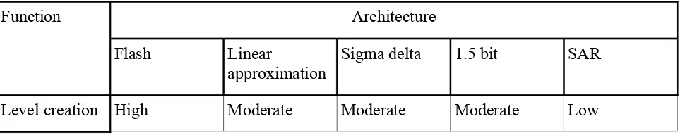
The amount of energy required for level creation depends on the amount of levels that need to be created and on the creation mechanism. Table 1 contains a qualitative comparison of energy requirements between several architectures.
VINPUT +
- VHOLD
-Function Architecture
Flash Linear
approximation
Sigma delta 1.5 bit SAR
Level creation High Moderate Moderate Moderate Low
Table 1: Qualitative comparison of level creation energy requirements
5.4 Comparison
Levels created by level creation circuitry need to be compared. An ADC contains one or more comparators. The output of an ideal comparator is amplitude discrete and uniquely determined by its inputs. Imperfections, their effects and the subsequent power dissipation are discussed in the following paragraphs.
5.4.1 Comparator imperfections
The main imperfections of a comparator are its limited speed and its inaccuracy. The magnitude depends on comparator architecture, technology limitations and fundamental limitations. Inaccuracy can be divided into offset and noise. On a system level these can best be described as input-referred quantities.
Offset and a limited speed are a direct result from technology limitations. Maximum speed depends mostly on the presence of parasitic capacitances. Noise is a fundamental limitation. In addition to fundamental noise a comparator can both generate and be sensitive to supply noise. Supply noise is an engineering issue.
5.4.2 Effects of comparison imperfections
The system level effects of comparator inaccuracies depend heavily on the ADC architecture. The speed of a comparator can limit the conversion speed of an ADC. This imperfection is mostly ignored for this project as discussed in paragraph 4.2.4.
For a SAR ADC the comparator offset is the ADC offset. This offset is acceptable for some applications as discussed in paragraph 3.5.2. Noise can be the limiting factor on the SINAD. In a sigma delta converter offset has very little effect on converter accuracy. Noise is shaped by a loop filter. A 1.5 bit converter uses an over-range mechanism such that offset and noise of the
comparators in the first stages do not affect the output. Comparator offset and noise in the last stage have little effect on the output due to the amplification in the previous stages.
A flash ADC requires 2Ncomparators for 2Ncomparisons. Both offset and noise of all comparators need to correspond to the full accuracy of the ADC. A linear approximation ADC also requires2N comparisons but needs only one comparator.
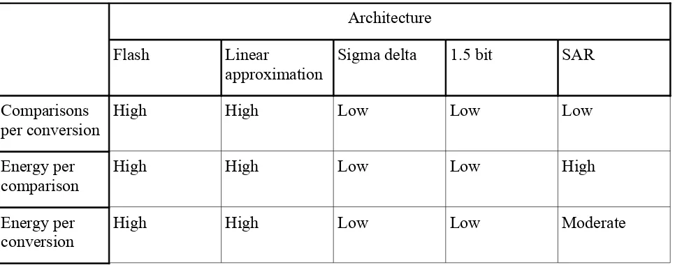
5.4.3 Comparison power dissipation
Architecture
Flash Linear
approximation
Sigma delta 1.5 bit SAR
Comparisons per conversion
High High Low Low Low
Energy per comparison
High High Low Low High
Energy per conversion
High High Low Low Moderate
Table 2: Qualitative comparison of comparison energy requirements
5.5 Digital circuitry
Digital circuitry can be required in an ADC control path. Additional digital circuitry can be required for the digital output. The first digital signals in an ADC are the comparison output signals. In paragraph 4.1.1 it has been decided that the output should use a common binary coding. Digital circuitry generates the common binary coding based on the comparison output. The complexity strongly depends on the ADC architecture.
The digital circuitry for a linear approximation ADC commonly contains a simple binary counter. This counter also provides a common binary coding. Therefore these three architectures can directly provide the desired ADC output.
The comparison output in a flash ADC is a thermometer coded value. Due to comparison errors there can be a bubble, an inconsistency in the code. As a result multiple comparison outputs map onto the same ADC output. The same is the case in an ADC with over-range, like a 1.5 bit
converter. For flash and over-range converters simple combinational logic is required to recode the comparison output.
The serial comparator output of SAR ADC is a common binary coding. The serial comparator output of a sigma delta ADC could also be argued to be a common binary coding. A decimation filter is required if it is desired to convert the sigma delta output to the same common binary coding as other converters.
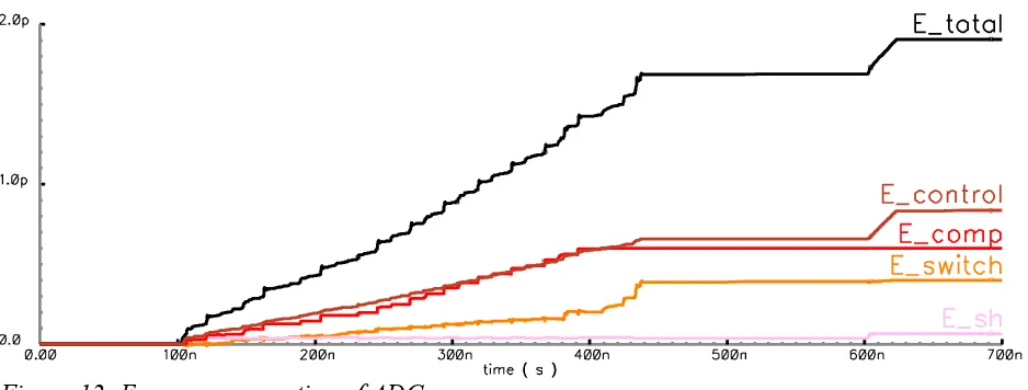
Energy dissipated in the digital circuitry depends both on the complexity and the amount of required digital processing. Table 3 contains a qualitative comparison of energy requirements between several architectures. For the sigma delta converter it is assumed that a decimation filter is not required. If it is, the energy requirements would be high.
Function Architecture
Flash Linear
approximation
Sigma delta 1.5 bit SAR
Digital circuitry
Moderate Moderate Low Moderate Low
More advanced schemes for digital error correction can be implemented, including digital data analysis. Such schemes are basically implemented on top of a basic architecture and are therefore not taken into account in this architecture comparison.
There are some general methods to decrease power consumption of digital circuitry at the cost of speed. The dominant power consumption usually results from charging and discharging all parasitic capacitances. The parasitic capacitances can be minimized by using the smallest allowed feature sizes for all transistors. In formula (10) it can be seen that the energy is proportional toV2 .
Consequently a reduction of the supply voltage can reduce the energy consumption.
Energy is also dissipated during the time that the digital input of a digital cell is in between the supply voltages. This dissipation can be reduced by reduction of the supply voltage too. If further reduction of the supply voltage is undesirable transistors with a high threshold voltage can be used.
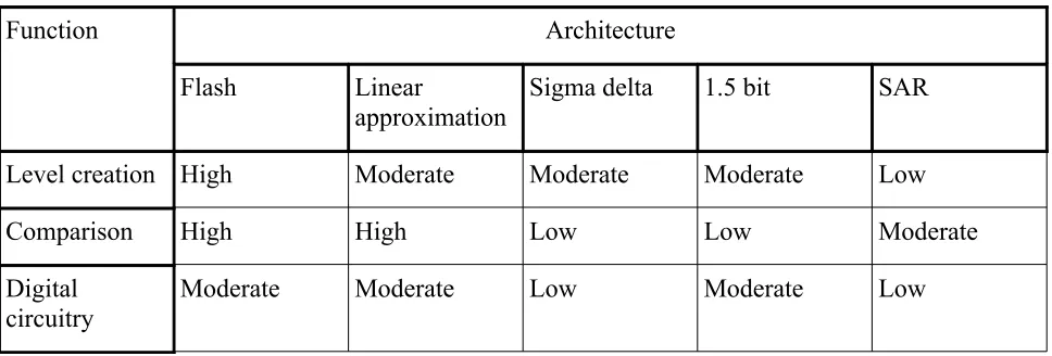
5.6 Comparison of architectures
Function Architecture
Flash Linear
approximation
Sigma delta 1.5 bit SAR
Level creation High Moderate Moderate Moderate Low
Comparison High High Low Low Moderate
Digital
circuitry Moderate Moderate Low Moderate Low
Table 4: Qualitative comparison of energy requirements
6 Low-power successive approximation ADC
First the basic principle of a successive approximation ADC is discussed in paragraph 6.1. Next techniques on the converter architecture level are discussed for potential comparison energy reduction in paragraph 6.2. Paragraph 6.3 discusses charge redistribution level creation and techniques to potentially reduce energy dissipation for it. A new energy-efficient comparator is introduced in paragraph 6.4.
6.1 Basic principle
Figure 2 contains a diagram of a basic SAR ADC. Prior to an actual conversion there is a sample-and-hold operation and the register is reset to contain only zeros. First the most significant bit (MSB) is tested. This is done by initially setting the MSB of the DAC to one and then comparing if this is either an over-estimation or an under-estimation. The result is stored in the MSB position of the register and consequently the MSB of the DAC is set for the rest of the conversion. The same procedure is followed for all other bits, from most significant to least significant. After N
comparisons the register contains the output of an N bit conversion.
Figure 2: Diagram of a basic SAR ADC
The name of the register, successive approximation register, is commonly used to identify the whole converter. Note that the DAC in the converter requires one less bit than the full ADC.
6.2 Comparison energy reduction
The main weak point of the SAR architecture compared to the sigma delta and 1.5 bit architectures is that every comparison needs to be done at the full ADC accuracy. Architecture level techniques that can possibly reduce the comparison energy will be discussed.
6.2.1 Over-range
A 1.5 bit ADC requires less accurate comparisons than a basic SAR ADC because it uses an over-range mechanism. It is possible to extend a SAR ADC with an over-over-range mechanism without requiring the same analog addition and multiplication as a 1.5 bit converter. This can be done by connecting several different SAR converters in parallel.
First all converters need to sample the same analog input value. They can all sample independently or use one combined master SH circuit. Next the least accurate SAR ADC performs a conversion. A sub-range of the full ADC input range is determined which includes the input value. From the point of view of the first SAR ADC this sub-range is an over-range, because is larger than its least-significant-bit (LSB).
The next SAR ADC is more accurate than the first one. The range of this converter is the
determined sub-range. An arbitrary number of converters can be used subsequently. Only the last converter needs to operate at full accuracy. Because of the over-range mechanism multiple outputs map on the same digital output value. Some combinational logic is required to construct the desired
SH
DAC Comparator
digital output.
A less accurate ADC can use a less accurate comparator, using less energy per conversion. In addition the level creation circuitry can also be less accurate.
As discussed in chapter 3 processing energy is an exponential function of the accuracy. As a result the energy consumption of the last SAR ADC is dominant. A theoretical energy reduction by a factor of almost N is possible.
Because the consumption in the last ADC is dominant it can be expected that additional energy savings are insignificant if more than two or three parallel converters are used. By further increasing the number of converters the change in energy consumption will depend on the resulting digital complexity.
6.2.2 Smaller average number of comparisons
The Hartley formula (15) gives the maximum amount of information that can be represented by a symbol that has sdiscrete possibilities. In an ADC a symbol is a sample and thesdiscrete
possibilities are the 2Npossible input level ranges. The condition that for every symbol alls
possibilities have the same chance of occurring corresponds to a uniform amplitude distribution and no time correlation. The standard SAR algorithm corresponds to a block encoding which is optimal if this condition is met.
For a practical input signal the condition is often not met and the SAR algorithm is not necessarily optimal. Before and during a conversion the sample can usually be predicted with some accuracy. A simple prediction can merely be based on a known amplitude distribution. For a more advanced prediction the previous samples and autocorrelation function can also be taken into account.
In the standard SAR algorithm every comparison reduces the sample range by 50%. The algorithm would add the maximum amount of information per comparison if a one and a zero would have the same chance of occurring. For a practical input signal this is often not the case. The algorithm can be adapted to add more information per comparison.
In such an adapted SAR algorithm the sample range is not necessarily reduced by 50%. For example it can be reduced by either 10% or 90% based on the comparison. Either way a larger amount of information is added than the expected amount of added information of the standard algorithm.
In 1951 Huffman developed an algorithm to group together the sdiscrete possibilities based on their chance of occurring. He proved this algorithm to be optimal. For an ADC his optimality corresponds to the smallest number of average comparisons required. Huffman coding can combine any possibilities based on their chance of occurring. In an ADC there is the added restriction that the range can only be divided in two ranges smaller and larger than a certain value. As a result the adapted SAR algorithm is not necessarily as efficient as Huffman coding.
A practical implementation can have some similarities with the over-range implementation as described in paragraph 6.2.1. In the over-range case an accurate converter only examines a sub-range. In the adapted SAR algorithm a sub-range is examined first and only if the sample turns out not to be within this sub-range a larger range is examined. It is like a bottom-up approach instead of the top-down-like approach of the standard SAR algorithm.
time plus some margin instead. This can actually result in a faster ADC for the same number of building blocks.
Just like an over-range converter a converter based on a smaller average number of comparisons requires more complex digital circuitry. Its energy consumption is likely higher than in a standard SAR ADC. However if the circuitry is designed event-driven most of the logic gates will not contribute to the energy consumption and the average energy consumption can still be low. Furthermore it can be expected that implementation becomes more favorable as processes scale.
6.2.3 Over-sampling
Both comparator noise and quantization noise are white. Sampling causes all noise to fold to half the sampling bandwidth. Consequently a result of over-sampling is that less noise folds to the original bandwidth. Over-sampling with a factor of n reduces noise power in the band of interest by a factor of n. For example four times oversampling yields one extra bit at the cost of four times more power. This is practically the same increase in power as would be required to get one extra bit of accuracy without over-sampling. Therefore over-sampling by itself does not reduce comparator energy.
When coherent ADC applications is not required the relevant clock generation specification is on period jitter, as discussed in paragraph 4.3.2. For a constant oscillator power and efficiency the absolute period jitter is lower when the output frequency is increased. As a result over-sampling can reduce the effect of clock noise on ADC accuracy.
Other effects of over-sampling have not been taken into account in this consideration. These include linearity, overhead and flicker noise.
6.2.4 Over-sampling with feedback
A sigma delta ADC is an example of an ADC that uses over-sampling in combination with
feedback. Every comparison output enters a feedback loop. Normal over-sampling with a factor of n reduces noise power in the band of interest by a factor of n. The loop filter of a sigma delta ADC shapes more of the noise to outside the band of interest. It is called noise shaping and allows a sigma delta ADC to use less accurate comparisons than a SAR ADC.
As discussed in chapter 5 there is a disadvantage of a sigma delta ADC compared to a SAR ADC in its level creation energy. This is because of its analog feedback loop. The loop can be a higher load for a DAC than a comparator and the loop itself dissipates energy.
It is theoretically possible to move the feedback loop to the digital domain. The resulting ADC would be a hybrid of a sigma delta ADC and a SAR ADC. Its basic diagram would be like figure 2 where the register is replaced by a more complex digital block.
The feedback loop is more or less approximating the current sample. In that regard it is similar to reducing the average number of comparisons as described in paragraph 6.2.2. Depending on the input signal the optimal feedback filter is most likely not linear.
The main disadvantage of this hybrid is that the inherent linearity of a one bit DAC is more difficult to achieve for a high resolution DAC as required in this hybrid. A solution could be sought in the directions of calibration or digital data analysis. This is a recommendation for future work.
6.3 Charge redistribution level creation for SAR
output is suitable for a capacitive input, like the gate of a MOST. Various comparator architectures exist with such an input.
6.3.1 Two-capacitor architecture
A charge redistribution architecture based on two equally sized grounded capacitors has been described in literature in 1974 [3]. The same authors wrote an improved paper in 1975 [4]. One of the capacitors is alternating switched to one of two references and to the other capacitor.
A digital-to-analog conversion always starts with the least significant bit and finishes with the most significant one. This order is reversed compared to the SAR algorithm.
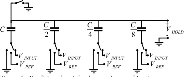
6.3.2 Traditional weighted-capacitor architecture
A charge redistribution architecture based on binary weighted capacitors has been described in literature in 1975, partially by the same authors who described the two-capacitor architecture [5]. The top terminals of all capacitors are connected together. A diagram of the traditional weighted-capacitor architecture is shown in figure 3.
Figure 3: Traditional weighted-capacitor architecture
During hold mode all bottom terminals are connected to one out of two reference voltages. In figure 3 the ground terminal is one of the two references. During redistribution mode the bottom terminal of one of the capacitors will be switched from one reference to the other. This capacitor is called the control capacitorCcontrol. There can be a parasitic capacitance between the combined top terminal and other nodes. In equation (33) the total capacitance is subdivided into four corresponding categories.
Ctotal=Cref1Cref2CcontrolCparasitic[F] (33) The voltage at the combined top terminal will now deterministically be modified by switching from one reference to the other. The change is a linear function of the difference between both reference voltages, formula (34). Note that not the shape of its path but the magnitude of the voltage
influences the change in output voltage.
VHOLD=±VREF⋅
Ccontrol Ctotal
[V] (34)
An implicit control voltage can be defined. It is the voltage at the bottom terminal of the control capacitor. The voltage drop over parasitic switching resistances is the difference between the reference voltages and the implicit control voltage.
During the sample mode of a SAR based on this architecture all bottom terminals are connected to the input voltageVINPUTand the top terminal is connected to a reference voltage. To go from sample mode to hold mode first the top terminal is disconnected. Next the MSB capacitor is connected to
C VHOLD
+ -C
2
C
4
C
8
VINPUT VREF
VINPUT VREF
VINPUT VREF
the positive reference while all other capacitors are connected to the negative reference. Energy is dissipated in the level creation even before the first comparison.
The top terminal is both during sample mode and at the end of the conversion at a voltage close to the reference voltage. A resulting advantage is that there is hardly a gain error introduced by parasitic capacitances.
A disadvantage is the complex switching for the sample-and-hold operation. It needs to be possible to connect every bottom capacitor terminal to both reference voltages and the input voltage. For low distortion it is important that input resistance and switch-timing are sufficiently level-independent.
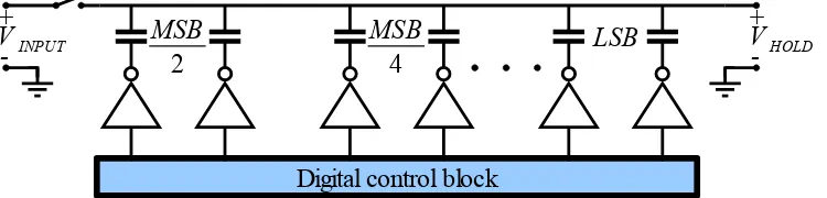
6.3.3 Alternative weighted-capacitor architecture
The complexity of the sample-and-hold operation can be reduced by directly sampling the input voltage on the top terminal. The switching complexity for a bottom terminal can be as low as an inverter.
A disadvantage of the traditional weighted-capacitor architecture is that energy is dissipated in the level creation even before the first comparison.
This first step can be avoided by a level shift of the reference. It is now possible to replace the MSB capacitor by a second set of binary weighted capacitors. Initially all capacitors within a set are connected to the same reference. The two sets start at opposite references. Now any next step in the SAR algorithm requires exactly one bottom terminal to change its reference. Figure 4 shows the alternative architecture.
Figure 4: Alternative weighted-capacitor architecture
The figure contains a diagram of the alternative weighted capacitor level creation architecture, including the location of the sample-and-hold switch and a digital control block. The digital control logic is slightly less complex than that in a traditional weighted-capacitor architecture. A first reason is the reduced complexity of the sample-and-hold operation. A second reason is that it is never necessary to switch back a bit that has been switched on for testing as part of the basic algorithm.
6.3.4 Accuracy through settling
Formula (34) assumes that the reference voltages are constant and do therefore not act like
additional control voltages. In reality fluctuations in reference voltages influence the hold voltage the same way the control voltage does. Instantaneous hold voltage accuracy depends on
instantaneous accuracies of the reference voltages. One of the factors influencing the accuracy of a reference is its output current. This current depends on the load.
During redistribution mode the load is not necessarily well defined. During hold mode it is dominantly capacitive. This is true for all charge redistribution architectures. Redistribution can temporarily disturb the accuracy of a reference. In fully settled hold mode there is no current. By allowing some time for settling the accuracies of the references and consequently the hold voltage can be improved.
Digital control block
MSB
2 LSB
VINPUT +
- VHOLD
+ -MSB
Because of the lack of current the references do not deliver any power during hold mode. This property makes charge redistribution architectures attractive for low-power analog-to-digital conversion.
6.3.5 Dissipation during charging and discharging of capacitors
During the redistribution mode of a two-capacitor circuit the load on the control voltage is one of the capacitors. For a weighted-capacitor circuit all capacitors except for the control capacitor are switched in parallel with each other. The control capacitor is switched in series with all other capacitances. The resulting load on the control voltage behaves like one capacitor.
For all architectures charge needs to be added to or removed from a real or equivalent capacitor. The most simple way to charge or discharge a capacitor is to switch a capacitor terminal from one voltage source to another, as shown in figure 5.
Figure 5: Simple circuit for charging and discharging a capacitor
Energy can only be dissipated in resistances. Most of the dissipation occurs in the parasitic
resistances of the switches. The magnitude of the dissipation depends on the capacitance and on the voltage difference. Formula (10) can be used.
A common mode does not influence the amount of dissipation. It does however add some complexity to calculations based on conservation instead of on dissipation. In these calculations voltage sources can deliver energy to each other.
6.3.6 Reduction of dissipation
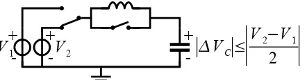
Energy dissipation happens in resistances and depends quadratically on the voltages across them (9). DC/DC conversion techniques can reduce these voltages. Application can result in considerable less dissipation during charging and discharging of capacitors. One possible technique uses an inductor in series with the switch and the capacitor, as shown in figure 6.
The circuit is shown in a DC steady state, with the top terminal of the capacitor directly connected to one of the voltage sources. A three-phase mechanism is required to charge or discharge the capacitor fromV1toV2.
Figure 6: Circuit for charging and discharging a capacitor
The first phase is shown in figure 7. The initial large voltage difference that would otherwise be over a parasitic resistance is now over the inductor. The inductor stores energy. The phase ends when the change in capacitor voltage is halfway in betweenV1andV2 . This moment depends on
the values of the inductor and the capacitor. It does not depend on the DC voltage levels. It can be determined by timing.
V2 +
-+
-V1 +VC=V1
-V2 +
-+
-Figure 7: First phase of a charging or discharging operation
The second phase is shown in figure 8. During this phase the energy stored in the inductor is used to further charge or discharge the capacitor. When the capacitor voltage has reached approximately the correct level the second phase ends. This takes the same amount of time as the first phase and can be determined by timing.
Figure 8: Second phase of a charging or discharging operation
The third phase is shown in figure 9. At the start of this phase there is no more energy stored in the inductor. It can therefore be short circuited without energy loss. The circuit enters another DC steady state. The conversion efficiency depends on the accuracy of the timing. The capacitor voltage accuracy does not depend on the timing. It depends on the accuracy of the references.
Figure 9: Third phase of a charging or discharging operation
An alternative DC/DC conversion technique is step-wise and uses a number of voltage levels in between both reference voltages. It is shown in figure 10.
Figure 10: Another circuit for charging and discharging a capacitor
To charge or discharge the capacitor fromV1toV4it is subsequently connected toV2 ,V3andV4. When appropriate intermediate levels are used every individual voltage step is small, reducing the voltages across resistances. The energy dissipation in this specific example can be calculated by formula (35). The general case fornequidistant steps can be calculated by formula (36).
E=12⋅C⋅
V1−V22V2−V32V3−V42
[J] (35)E=1 2⋅C⋅n⋅
V n
2
= 1
2⋅n⋅C⋅V
2
[J] (36)
The conversion efficiency depends on the number and accuracy of the intermediate voltages. The capacitor voltage accuracy does not, it comes directly from the references. If the same intermediate voltage sources are used for both charging and discharging they can be implemented by large capacitors to any supply voltage. During use their charge will automatically converge to appropriate levels.
∣
VC∣
≤∣
V2−V12
∣
V2 + -+-V1 +
-∣
V2−V12
∣
≤∣
VC∣
≤∣
V2−V1∣
V2 +
-+
-V1 +
-V2 + -+
-V1 +VC=V2
-+
-V1 +VC=V1
-+
-V2 +
Both DC/DC conversion techniques are best suited for changing a voltage from one reference to another. Applying them to a weighted-capacitor charge redistribution architecture is
straightforward.
The first stage in a two-capacitor architecture charges or discharges from any of many intermediate voltages to a reference voltage. The second stage shorts the two capacitors. As a result it is not so practical to apply either of the DC/DC conversion techniques.
In case of a differential implementation of a weighted-capacitor charge redistribution mechanism two equivalent capacitors need to charge or discharge at the same time. These equivalent capacitors are of equal size and in fact need to swap their charge. A two-phase DC/DC conversion technique similar to the three-phase inductor based single ended technique can be implemented. During the first phase an inductor is temporarily switched in between both equivalent capacitors. During the second phase the equivalent capacitors are switched towards their new references.
6.3.7 Thermal noise lower limit on capacitor value
When a voltage is sampled onto a capacitor thermal noise causes an error voltage (8). For application in an ADC this error voltage needs to be related to the LSB voltage, for example by equation (37). The LSB voltage is related to the total range of the converter (38). Combining these equations gives a minimum value for the hold capacitor (39).
v
VLSB
2 [V] (37)
VLSB=VRANGE⋅2−N[V] (38)
C 4⋅k⋅T
VRANGE
2 ⋅4
N
[F] (39)
6.3.8 Matching lower limit on capacitor value
Mismatch between capacitors causes non-linear level creation. This is true for both two-capacitor and weighted-capacitor architectures. In this section the non-linear behavior of weighted-capacitor architectures is considered. Similar to what was done in paragraph 6.3.7 the error voltage is related to the LSB voltage and a minimum value for the capacitor is calculated.
Equation (40) is a simplified version of equation (33) and equation (41) is based on (34). The relative output voltageVreldepends on the fractionChofCtotalthat is connected to the high reference voltage. Its range is from 0 to 1.
Ctotal=ChCl[F] (40)
Vrel= Vout
VRANGE=
Ch ChCl[]
(41)
The capacitor value variances of both capacitors are considered to be independent. This is used to calculate the variance in relative output voltage, formula (42).
Vrel
2
=
∂V ∂Ch
2
⋅Ch
2
∂V ∂Cl
2
⋅Cl
2
[ ] (42)
directly results in formula (43). More elaboration results in formula (44).
Vrel
2
=
ChCl−Ch ChCl2
2
⋅AC2⋅Ch
−Ch ChCl2
2
⋅AC2⋅Cl[ ] (43)
Vrel
2
= Cl2⋅Ch ChCl4⋅AC
2
Ch2⋅Cl ChCl4⋅AC
2
[] (44)
Formulas (40) and (41) are used to simplify formula (44). This results in formula (45) and with some more elaboration in (46). Note that the variance is zero for a relative voltage of 0 or 1. This corresponds to the strict definition of the INL. Therefore it is an overestimation for the calculation of the FOM as discussed in 3.5.2.
Vrel
2
=1−Vrel
2
⋅Vrel⋅
AC2
CtotalVrel
2
⋅1−Vrel⋅
AC2
Ctotal[ ] (45)
Vrel
2
= AC
2
Ctotal⋅Vrel−Vrel
2
[] (46)
In formula (46) the variance in relative voltage depends on the relative voltage. If the probability density ofVrelis known the expected value ofVrel
2
can be calculated. Formula (47) is based on a uniform probability density.
EVrel
2
=
∫
Vrel=0Vrel=1
AC2
Ctotal⋅Vrel−Vrel
2
d Vrel= AC
2
6⋅Ctotal[] (47)
The variance in capacitor value is a stochastic process. However it is generally not stochastic in between the creation of various levels. This is because there is only one realization which is determined at the time of manufacturing. As a result the actual variance is smaller in some circuits and larger in others. Several techniques exist to make sure that the variance is smaller than a desired maximum value.
A first technique is arranging the realization to be stochastic in between the creation of levels. This requires all capacitors to interchange roles in a manner unrelated to the signals being processed. A second technique is calibration.
A third technique is static matching. It is assumed that the actual value is a number of times larger than its standard deviation. Parameters are chosen in such a way that the circuit works within specification for the larger value. When the actual value is even larger the circuit has failed proper manufacturing and is scrapped. In equation (48) the parameter is called M.
M⋅Vrel=
M⋅AC
6⋅Ctotal[] (48)M⋅Vrel⋅VRANGE
VLSB
2 [V] (49)
M⋅AC
6⋅Ctotal2−N1[ ]
(50)
Ctotal23⋅M2
⋅AC2
⋅4N
[F] (51)
Calculating an actual minimum value requires numerical values forM,ACand N. The value in (52) is based on 3matching, 1% mismatch for a 1fF capacitor and a 10 bit converter.
Ctotal 2 3⋅3
2
⋅10−19⋅410≈630[fF] (52)
6.3.9 Comparison of lower limits
A lower limit on the capacitor value has been determined for thermal noise and for matching. Which of the effects is dominant depends on the parameters. From (39) and (51) it can be derived that the effects are equal under condition (53). As expected there is no dependence on the number of bits. In (54) the parameters have been replaced by values that can be argued to be realistic for a current project. Mismatch is dominant over thermal noise if the converter range is larger than this value.
VRANGE=
6⋅k⋅TM⋅AC
[V] (53)
VRANGE≈
6⋅1.38⋅10−23⋅3003⋅10−9.5 ≈170[mV] (54)
6.4 Comparator
As discussed in paragraph 5.4.2 the most relevant property of a comparator for a basic SAR ADC is its input-referred noise. Speed and offset are of less importance.
6.4.1 Architectures
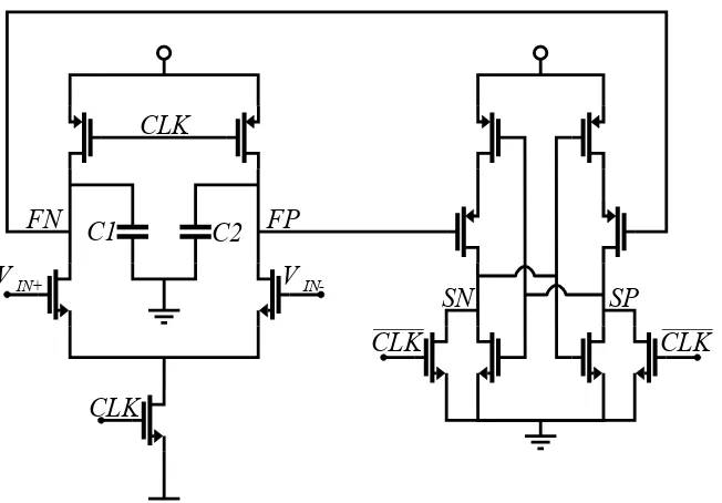
Comparator architectures exist with and without a bias current and with and without an externally applied clock signal. An example of a comparator with a bias current and without a clock signal is a high gain differential voltage amplifier. The high gain results in an output that can clip to one of the supply voltages. This traditional approach is still in use [1].
Other comparators use an externally applied clock signal to activate a positive feedback mechanism within an amplification stage. The result is an output that has more reliably assumed a valid digital value. The reliability depends on the gain, the capacitance and the time [6].
A new comparator architecture without a bias current and with an externally applied clock signal has recently been developed as part of the nano-wire project [2]. It has a high speed and a
6.4.2 New comparator topology
As part of this project yet another new comparator architecture has been developed. It is based on the comparator of the nano-wire project. It is shown in figure 11.
Figure 11: Schematic of new comparator
Like the nano-wire comparator it consists of two stages. Contrary to the first stage of the nano-wire comparator explicit capacitors have been added to nodes FNand FP. The second stage uses a pair of PMOS transistors within the cross coupled inverters. The nano-wire comparator uses NMOS transistors parallel to the inverters, leading to faster regeneration.
Both comparators can cause some co