i
,
..
Univac@
LARC
COMPUTING
UNIT
INSTRUCTION SEQUENCE
CONTROL
PART 1
~Rnnd~~
DIVISION OF SPERRY RAND CORPORATION
AUGUST 1961
RESTRICTED DISTRIBUTION
Univac®
LARC
COMPUTING
UNIT
INSTRUCTION SEQUENCE
CONTROL
PART 1
CONTENTS
Heading Title Page
SECTION 1. INTRODUCTION
1-1. Basic Concept of Instruction Control in the
Computing Unit. • • • • • • • • • • 1-1 1-2. Scope of This Book • • • • • • • • • • • • • 1-2
SECTION 2. CONTROL OF THE BASIC INSTRUCTION CYCLE
2-1. 2-2. 2-3. 2 .. 4.
2-5. . 2-6.
2-7. 2-8. 2-9.
3-1. 3-2.
3-3. 3-4.
3-5. 3-6. 3-7.
3-8. 3-9.
3-10.
3-11. 3-12. 3-13.
4-1. 4-2.
Basic Instruction Cycle
.
.
.
Instruction Call • • • • • • • • • • • B-Modification • • • • • • • • • • • • Operand Select
Execution • • •
.
.
. .
.
.
Store Result • • • • • • • • • • Normal Continuous OperationInitial Instruction Request • • • • • • Overlapped Instruction Sequencing
SECTION 3. INSTRUCTION SEQUENCE CONTROL
Fast Register Chain Control • • • • • • • • Fast Repister Input Chain Control • Fast Hegister Result Chain Control •• Operand Memory Reference Control • •
Program Counter Control •• • • • •
Special Instruction Sequence Control Cases • Memory Busy on Operand Call • •
Memory Busy on Instruction Call
Long Instructions • • • • • • • • • • • Double-Precision Instructions •
Fast Register Access Conflicts • • Operand Reference (A Register) ••
Address Modification (B Register)
SECTION 4. SUMMARY OF ENDING PULSE FUNCTIONS
Instruction Ending Pulse • • • • • • • • • • Ending Pulse Functions for Normal Continuous Operation • • • • • • • • • • • • • • • •
2-1 2-2 2-4 2-4 2-7 2-7 2-7 2-11 2-11
3-1
3-2 3-9 3-11
3-16
3-18 3-18 3-20 3-22
3-25 3-27
3-30 3-31
4-1
iv Heading 4-3. 4-4. 4-5. 4-6. 4-7. 4-8. 5-1. 5-2. 5-3. 5-4. Title
Ending Pulse CHJQ-2 • • • • • • • • Ending Pulse CHJQ-3 ~ • • • • • • • Ending Pulse CHJQ-l • • • • • • • • • • Ending Pulse Functions for Noncontinuous
Operation • • • • • • • • • • • • • • • • Ending Pulse Functions for No-Overlap Mode • . Ending Pulse Storage Flip-Flop • • • • • • •
SECTION 5. INTRODUCTION TO STATUS CONTROL
Status Control • • • • • • • • • Status-l Flip-Flop • • • • •• • Status-2 Flip-Flop • • .'. • • • Status-3 and Status-4 Flip-Flops
· . . .
.
.
·
. .
·
.
·
. .
. . .
SECTION 6. CLASSIFICATION OF INSTRUCTIONS
ACCORDING TO CONTROL FEATURES
Page 4-2 4-2 4-3 4-4 4-4 4-5 5-1 5-2 5-3 5-3
SECTION 7. NONCONTINUOUS AND NO-OVERLAP OPERATIONS
7-1. 7-2. 7-3. 7-4. 7-5. 7-6. 7-7. 7-8. Figure 2-1. 2-2. 2-3. 2-4. 2-5. 3-1. 3-2.
Noncontinuous Operation
·
•· ·
•· · ·
•·
Start After General Clear •
·
•·
•·
•·
•
Stop in Continuous Mode •·
•·
• •·
•·
• One-Instruction Mode •·
• • • •· ·
•· ·
•Multivibrate Mode
. . ·
·
•· · ·
• •No-Overlap Mode
.
•.
·
· · · ·
•·
•·
•·
No-Overlap Continuous Operation • • • •
No-Overlap Interrupted Operation
· · ·
ILLUSTRATIONS
Title
Simplified Control Block Diagram • • • • • • Timing Diagram -Basic Instruction Cycle •• Timing Diagram - Instruction Overlapping • • Simplified Logic Diagram - Instruction
Re-quest Cycle • • • • • • • • • • • • • • • Timing Diagram - Normal Continuous Operation
Simplified Logic Cycle • • • • Simplified Logic Chain Control
Diagram - Normal Instruction
• • • • .• • • • • • • • • e'
Diagram - Fast Register
Figure Title Page
3-3. Timing Diagram - Fast Register Input Chain
Control • • • • • • • • • • • • • • • • • 3-8 3-4. Timing Diagram - Fast Register Result Chain
Control • • • • • • • • • • • • • • • •• 3-10 3-5. Simplified Logic Diagram - Operand Memory
Reference Control • • • • • • • • • • • • 3-12 3-6. Timing Diagram - Memory Reference Control,
Read • • • • • • • • • • • • • • • • • • 3-14
3-7. Timing Diagram - Memory Reference Control,
Write • • • • • • • • • • • • • • • • •• 3-15 3-8. Simplified Logic Diagram - Program-Counter
3-9.
3-10.
3-11. 3-12.
3-13. 3-14.
3-15.
5-1.
5-2.
1-1.
1-2.
1-3.
1-4.
Table
Control Circuits • • • • • • • • • • Timing Diagram - Memory Busy on Operand
Call • • • • • • • • • • • • • • • • • • Timing Diagram - Memory Busy on Instruction Call • • • • • • • • • • • • • • • • • • Timing Diagram - Long Instruction • • • • • Timing Diagram - Double-Precision
Instruction • • • • • • • • • • • • • • • Timing Diagram - Fast Register References • Timing Diagram - B-Register Conflict at
t3 . • . . • . . . • . Timing Diagram - B-Register Conflict at
t7 . . • . . . .
Simplified Logic Diagram - Status Control Flip-Flops • • • • • • • • • • • • • • • Timing Diagram - Status Control • • • • • •
Simplified Logic Diagram - Noncontinuous Operation Controls • • • • • • • • • • • Timing Diagram - Stop in Continuous Mode • Timing Diagram - Restart After Stop • • • • Timing Diagram - No-Overlap Mode • • • • •
TABLES
Title
6-1. Classification of Instructions
.
. .
. . .
3-11
3-19
3-21 3-23
3-26 3-29
3-32
3-34
5-2 5-4
1-2 1-5
1-6
1-11
Page
SECTION 1
INTRODUCTION
1·1. BASIC CONCEPT OF INSTRUCTION CONTROL IN THE COMPUTING UNIT
The control unit is the coordination center for the computing unit. The principal function of the. control unit is to control the acquisition and sequencing of several instructions in parallel. Parallel operation is achieved through the technique of overlapped instruction execution wherein several instructions are in various distinct phases of execution at anyone time. The maj or logic elements wi thin the instruction control circuits are used on a time-shared bases which imposes rigid timing considerations in the performance of control uni t functions. These maj or logic elements in-clude two instruction registers, two control counters, two memory address-decoders, two fast register selector registers, a fast register decoder, a program counter, an instruction decoding-encoding network, and several con-trol flip-flops.
The term "instruction cycle" denotes the series of functions performed by the control unit to address, obtain, and decode instructions from the memory; to acquire operands from core memory and fast r~gisters; to perform arithmetic and logical operations on the operands; and to return the re-suI ts to storage. Performance of the complete series constitutes a "normal" instruction cycle and is executed automatically in the control unit for several instructions in a program sequence at the same time. The control unit will alter the cycle in accordance with the execution of certain in-structions such as control transfers. Whenever a transfer of control takes place, the overlapped instruction sequencing is temporarily interrupted but is continued upon completion of transfer.
Instruction overlapping can result in. various conflicts from time to time that cause delays in the sequencing. For example, an addressed memory unit may be already engaged with a previous operation, or the result of one instruction may not be available in time if it is required for use in the
~ 0Ep~i n~
t
pSJ;t"H.9 t;fp.n,!:,COi{l,tli~C~,s; }l4;~* a~; \~l;l~ ~~'1:! ~~~~Pl,~;r~, r~sp:~iVe(t;~ u t0-1Il?,tl'Cf;,;
lrJ.~,...
the; ,~,onfJ:Rb
!:lP~t.;:7
Aa IJ.ll:f qr~9lI!PJ!~ ca:"1~,d ,~;pg;l",K,llecall{l ~ jqt;:F,~~':;;need to Introduce delays or repeat certain operations.' ,,;,:f,;: L:.
1-2. SCOPE OF THIS BOOK
Instruction sequence control is divided into two parts of which this book constitutes part I. A more or less general approach to the subject is taken in part I in which the overall aspects of instruction sequencing are described for the variety of conditions under which the control unit must operate. Part II is a continuation of part I and deals comprehensively with special instruction sequencing features related to store and control
transfer instructions and other control operations.
The primary purpose of this book is to provide detailed information on the timing of instruction sequence control operations in the control unit. A familiarity with the essential features of the computing unit is assumed. The following three books provide additional related material on the con-trol unit:
(1) Computing Unit--General Description
(2) Computing Unit--Control Logic
(3) Computing Unit--Instruction and Function - Signal Analysis
This book is organized to take the reader progressively through the timing of operations in the control unit from the basic instruction cycle to the condition of full overlapped sequencing. The various control fea-tures associated with the logic. the timing, and the handling of special cases in the control unit are described separately throughout the book as outlined below.
Section 2 describes the basic instruction cycle for a single instruc-tion and then explains the overlap technique for executing a series of in-structions during normal continuous operation.
Section 3 deals comprehensively with most conditions of instruction sequencing in which different aspects of control and timing are covered for the majority of instructions in the computing unit repertory.
Section 4 summarizes the ending pulse functions for all types of oper-ation.
Section 5 presents an introductory discussion of instruction status control which is covered more fully in part II.
Section 6 classifies all the instructions in the computing unit reper-tory according to the control features described in sections 2 and 3. The principal inclusion in this section is a table which affords quick refer-ence to general control features associated with any particular instruction.
Section 7 describes the logic and timing associated with starting and stopping the computing unit and with the noncontinuous and no-overlap modes of operations.
SECTION 2
CONTROL OF THE BASIC INSTRUCTION CYCLE
2.1. BASIC INSTRUCTION CYCLE
The instruction cycle of the computing unit consists of five basic operations of the control unit which are carried out by the instruction con-trol logic. The names of the basic operations performed in all instruction cycles are:
(1) Instruction Call -- addressing the memory and receiving the next instruction in a program sequence in the instruction st0rage reg-ister (IRl).
(2) B-Modification -- performing index operation for current instruc-tion; that is, adding the contents of the designated B register to the M address contained in the instruction. to obtain the next (operand) storage reference address.
(3) Operand Select -- addressing the memory to select the M operand for the current instruction. Also addressing the fast registers to obtain the A operand and supply instruction information and operands to the arithmetic unit (AU). The latter operations are conditional on the former; that is, the fast register reference and the initiation of operations in the AU depend on the success-ful call to the memory (memory-not-busy signal received) for the M operand. If no operand memory reference is required for the current instruction, the effect of a successful memory call is simulated.
(4) Execution -- depending on the instruction, the execution phase is handled by the control unit or the AU. The unit not in use just marks time.
(5) Store Result store the result. for the current instruction.
considered as extending from time to through t7, is used as the principal time division in the timing diagrams in this manual and is hereinafter referred to simply as the cycle.
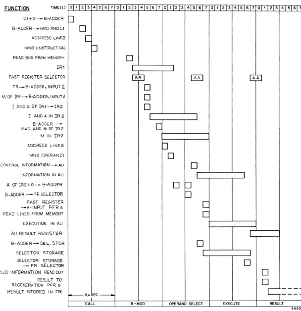
Each of the basic operations, except execution, normally takes one cycle to complete. The execution phase of an instruction takes one or more cycles to complete depending on the type of instruction. The total time required to process a single instruction, then, is at least 20 microseconds. However, the normal sequence of operations performed by the control unit is overlapped in time-so that the five basic operations may be carried out for five different instructions during anyone cycle. In this way a sequence of instructions which takes no more than one cycle of execution time in the AU can be performed at the rate of one instruction every 4 microseconds.
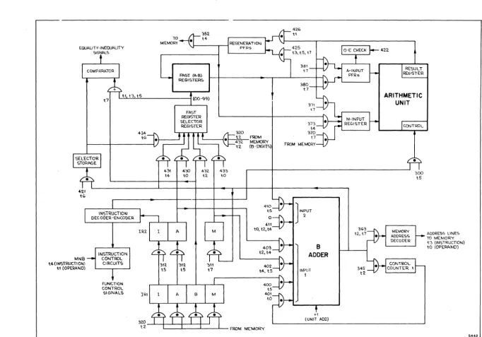
In order to explain the timing considerations involved in the overall operation of the control unit, a single instruction will be traced through all of the steps required to complete its execution. For this discussion, assume that the instruction is one of the common single-precision memory reference types; for example an add instruction which requires the minimum execution time of 4 microseconds. A simplified block diagram of the con-trol unit showing only the most basic timing and function concon-trol signals is given in figure 2-1. A timing chart covering five cycles corresponding to the five basic operations of the instruction cycle is presented in fig-ure 2-2. The chart also lists all the normal steps that are followed to complete the execution of an instruction.
2-2. INSTRUCTION CALL
To call the next instruction from memory, its address must first be established: the contents of control counter 1 (Cl) are sent to the B-adder as one input, and depending on the sequencing situation, a 0 or +1 as the other input. The two are added together to form the new address. For dis-cussion, assume that Cl already contains the address of the new instruction so that the constant to be added to Cl is a O.
The contents of Cl enter input 1 of the B-adder at time to with func-tion control signal 401 (FS401). The 0 enters input 2 with FS411 also at to. The two values, Cl + 0, are added in the B-adder during tl and the sum (next address) is read out to the memory address decoder (MAD) with FS363 at t2. The MAD partially decodes the new address and sends the information over the address lines to the memory at t3.
If the memory unit that is addressed by the current instruction call is not busy, a memory-not-busy control signal (MNB) will be generated in the memory unit and returned to the control unit at t4. If the MNB signal is not received at t4, delays will arise in the control unit and the in-struction call will have to be repeated. Assuming no delays, the instruc-tion will be read out from the memory during the 4-microsecond basic memory cycle and appear on the read bus from the memory during t2 of the next cycle.
At t2 of the second cycle, the instruction word is transferred to IRI with FS320j and at t3 the word is stored in flip-flops in IRI. The
divi-sions of IRI (It A, B, and M) shown in figure 2-1 accept the various parts of the instruction word. While the instruction is being transferred into
EGiJAlI TY -INEQUI>.UTY SlGNI>.LS
TO MEMORY
FI'6T (A-B) REGISTERS
L!:.t!lol -"t.::.3,~t,-,5:... _ _ _ _ _ _ ~ (00-99)
MNB t4-(INSTRUCTION) tl (OPERAND)
INSTRUCTION CONTROL
CIRCUITS
FUNCTION CONTROL SIGN"LS
434
tG
IRI
312-t5
FAST REGISTER SELECTOR REGISTE~
4:£)
to
312-tS
432
102
43, to
320
t1 FroM
432 MEMORY t~ (6-DlGITS)
410
t5
o
411
to, t2,
t4-403
t2, t4 B
ADDER
+1
(UNIT ADD)
345
t'2
RESULT REGISTER
ARITHMETIC UNIT
CONTROL
•
300t5
ADDRESS LINES
TO MEMORY
to (INSTRUCTIOI\I) to (OPERI>.ND)
IRI, the B part of the instruction word is transferred directly into the fast register selector register with FS432 and FS320 to start the B-modification (B-mod) portion of the instruction cycle.
2-3. B-MODIFICATION
The B register selected by the two B digits of the instruction word contains the information that will be used to index the current instruction. The designated B register is selected during t3 and t4 and the five least significant digits of the contents are sent with FS410 to input 2 of the B-adder at t5. The information in the B register is regenerated (FS425) and also sent to the A-input pulseformers of the AU for odd-even check
(FS380, 422).
Input I to the B-adder is supplied by the M part of IRI which is sent to the B-adder with FS400 at t5. The two inputs are added together during t6 and the sum is read out with FS363 to the MAD at t7. This new address is the modified M address which is sent across the address lines to the memory at to of the third cycle to select the M operand. The M address can specify a fast register in which case a memory call is not needed (refer-ence heading 3-2).
During the B-mod operation, the I and A parts of IRI are transferred to IR2 with FS312 at t5. At t7 the modified M address from the B-adder is also transferred to the M part of IR2 with FS311. IR2 now holds the I and A digits of the original instruction word and the modified M digits of the operand address. IR2 does not store the B digits of the instruction.
2-4. OPERAND SELECT
The decoding of the I digits is static during the time the instruction is in IR2. As shown in figure 2-2, this time extends from t6 of the second cycle through t5 of the third cycle. During this interval all necessary control signals peculiar to the instruction are generated so that specific functions may be carried out in the control unit. As mentioned under head-ing 2-3, the call to the memory for the M operand is made at to of the third cycle. If the memory unit is not busy, an MNB signal will be re-turned to the control unit at tl to indicate that the selected M operand will be available on the read bus at the next t7. The control information for the AU is then transferred from a separate function encoding network at t5 wi th FS300.
The A operand is selected by sending the A digits of IR2 to input I of the B-adder at t2 with FS403. Input 2 to the B-adder at this time is a 0 (FS411) so that the sum, A + 0, is read out to the fast register selector register at t4 with FS431. The reason for this apparently devious path in transferring the A part of IR2 to the fast register selector register is that in some instructions the A digits require a modification to their ori-ginal value.
The designated A register is selected during t5 and t6 and the con-tents are transferred into the A-input pulseformers of the arithmetic unit at t7 with FS380 and also regenerated with FS425. The M operand arrives simultaneously from the memory read bus and enters the M-input register of
FUNCTION TIME (t)
C~ + 0 - B-ADDER
B""ADDER---MAD AND C1
ADDRE3S LlNE.3
MN8 (IN5TRUCTION)
READ BUS FROM MEMORY
IR1
FAST REGISTER SELECTOR
FR-B-ADDER, INPUT
2-M OF IR~-B-ADDER, INPUT,1
1 A.ND A. OF" IRJ ---IR2
I AND A IN IR 2
BADOER -MAD AND M OF lR2
M IN IRZ
ADDRE5S liNES
MNB (OPERAND)
CONTROL INFORMATION - -AU
I NFORMATION IN AU
A OF lR2+0-8-ADDER
B-ADDER - FR SELECTOR
FAST REGiSTER -A-INPUT PFR 5
READ LINES FROM MEMORY
EXECUTION IN AU
AU RESULT REGISTER
B-ADDER-5EL. STOR.
SELECTOR STORAGE
SELECTOR STORAGE
- FR SE.LECTOR
0LD INFORMATION REtlD OUT RESULT TO RE:GENERATIOl-\ PFR s
RESULT STORED IN rR
01 11213 4151617 011 12L 3 4151617
~
D
L
0
0
I
em
0
D
0
I
C
4,. SEC I
CALL B-MOD
011 1213 4151617 01 11213 4151617 011 1213 41 51617
I
~ AA
I
P
0
D
I I
0
D
D
L
L
I
0
L I
0
0
D
C;----
-OPERAND SELECT EXECUTE RESULT
5443
the AU with FS370. At the following to (fourth cycle), the beginning of the instruction execution time (in this case 4 microseconds) in the AU is started.
2-5. EXECUTION
The execution of the instruction in the AU is carried out autonomously once the AU has received operands and instruction information from the con-trol unit. However, since IR2 is cleared before the execution takes place, it is necessary to preserve the result address for the instruction during the execution phase.
To select the correct A register to store the result, the A part of IR2, along with a 0, are again sent to the 8-adder at t4 of the third cycle. The sum A + 0 is formed and then transferred to the fast register selector storage at t6 with FS421. The selector storage holds the result address for the next 4 microseconds (t7 through t6 of the fourth cycle) while the instruction is being executed in the AU. At t6 the contents of the selec-tor sselec-torage are transferred to the fast register selecselec-tor register with FS434 so as to select the A register (t7, to) to receive the result from the AU.
2-6. STORE RESULT
The result portion of the instruction cycle takes place during the fifth cycle. The result of the operation is first stored in the result reg-ister of the AU from t7 through t3. The old information in the selected A register is read out at tl while the contents of the result register are transferred to the fast register regeneration pulseformers with FS426. The result is then written into the selected A register at t2. This operation constitutes a clear-write cycle for the fast register which is the same as the read-regenerate cycle carried out for operand selection except that FS426 -replaces FS425.
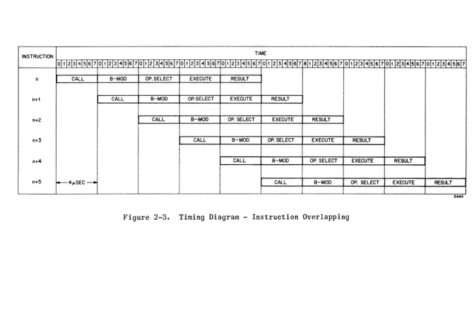
2·7. NORMAL CONTINUOUS OPERATION
The normal instruction sequence control in the computing unit operates in a continuous mode so that succeeding instructions in a sequence are overlapped in time throughout the various phases of the instruction cycle. Figure 2-3 illustrates the overlap principle by showing a series of in-structions passing through the five stages of the instruction cycle. The instructions are staggered by a period of 4 microseconds. When instruction n
+
4 is being called from the memory, the previous instruction n+
3 is having its M address modified, the operands for n + 2 are being selected, the arithmetic unit is executing n + 1, and the result of n is being stored. In the next cyclet n+
5 is called from memory, n+
4 is having its M ad-dress modified and so on.As mentioned under heading 2-1, the overlapping technique results in a considerable saving in the effective instruction execution time. However, because of overlap, various conflicts in the timing of operations within the control unit can arise which will from time to time result in some
r.." I
CO
INSTRUCTION
n
n+I
n+2
n+3
n+4
n-t-5
01 I 12 1*1*17
CALL
4 p . S E C
-TIME
01 I 12131 4 15161 7 01tlZl*15\617 0ltl21314151617 01 tj21314151617 01112131415161 7 elt 121314151617 0ltl 2 J3J 415j6j7 01tj2J314151617 011121314151617
B-MOD OP.SELECT EXECUTE RESULT
CALL B-MOD OP.SELECT EXECUTE RESULT
CALL B-MOD OP. SELECT EXECUTE RESULT
CALL B-MOD OP. SELECT EXECUTE RESULT
CALL B-MOD OP. SELECT EXECUTE RESULT
CALL B-MOD OP. SELECT EXECUTE RESULT
5444
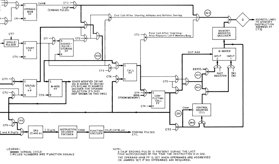
(FROM MEMORY) MNB CTt CHTB (GENERATED IF INSTRUCTION REQUIRES MEMORY ACCESS)
SIGNf..LS GENERATED IF NO [ MEMORY ACCESS REQUIRED
OR IF OPERAND ADDRESS IS A FAST REGISTE.R
PFR
Clear
8
lR1
S CHNB
OPERAND-MNB FF R CT7 CTt S START FF R CT2 CHJP (ENDING PULSE)
s
R B-MOD FF S ENDING- PULSE-STORAGE Ff Re
CT3~ ... ~ SENDS MODIFIED IR1 (M)
VIA B-ADDER TO IR2 (M)
(FS 311), AND TO ADDRESS DECODER FOR OPERAND SELECTION (FS 363)
(NOT SHOWN ON THIS DWG.)
2nd Call After Starting Initiates and Retains Overlap
.~---~~---~---~
CT2.
CT4
MNB
(FROM MEMORY)
First Call After Starting:
Also Repeats Call if Memory Bvsy .
CTO s COM- PLETING-CALL FF R
@
Unit f!.dd
Clear CONTROL COUNTER
(C 1)
IR2 I Digits
(I AND A)
INSTRUCTION '-C_H_S_A .... -.j fUNCTION CHJP, CHT8, etc:
DECODER- ~ ENCODER ENDING PULSES
ETC. ENCODER
LEGEND:
- NORMAL CYCLE
CIRCLED NUMBERS ~RE FUNCTION SIGNALS
NOTE:
A CHJP ENDING PULSE IS PRESENT DURING THE LAST FOUR MICROSECONDS OF THE TIME THE IN5TRUCTTON IS IN IR2.
THE OPERAND-MNB FF IS SET WHEN OPERANDS ARE ADDRESSED OR JAMMED SET IF NO OPERANDS ARE REQUIRED.
MEMORY ADDRESS DeCODER
B-ADDER
INPUT INPUT
2 1
ADDRESS LINES TO MEMORY (INSTRUCTION
/lDDRESS AT CT3)
5459
Figure 2-4. Simplified Logic Diagram - Instruction Request
Cycle
delays. These delays will be discussed .in section 3. The remainder of this section describes how overlapped instruction sequencing is controlled starting with the initial instruction request.
2~8. INITIAL INSTRUCTION REQUEST
A simplified logic diagram of the instruction request cycle is shown in figure 2-4. This figure shows the logic which controls the instruction request cycle by relating various control signals and flip-flops to the timing of overlapped instruction cyclesj certain recurrent details are as-sumed to repeat in each instruction. An accompanying timing diagram for these operations is given in figure 2-5. Although figure 2-5 shows timing relationships for continuous operation, it is simplified in that it does not show all the operational steps of the basic instruction cycle as out-lined previously in figure 2-2.
This description assumes that the computing unit is stopped and both instruction registers (IRI and IR2) are empty. Operation is initiated by pressing the START button on one of the control consoles. The first t7 timing signal then produces an output from the single-pulser circuit to set the start FF. The output from the start FF is gated with CTI to set the storage FF, and with CT3 to set the call FF. The ending-pulse-storage FF is used to provide for certain control functions that are nor-mally supplied by an instruction ending pulse during the last- 4
microseconds of the time an instruction is in IR2. Essentially it provides a substitute ending pulse for the one usually produced by the previous instruction (reference heading 4-8). The start FF is then reset at t5 since it is no longer relevant to the control cycle.
The output from the call FF is first used to produce function control signals 401 and 411 at to which send the contents of the control counter (Cl) and zeros to the B-adder at to. Cl contains the address of the first instruction (n). The sum Cl + 0 is then gated from the B-adder to the mem-ory address decoder by FS363 which is generated by gating the call FF out-put with CT2. Thus the first instruction call is on the memory address lines at t3. The MNB signal is generated during the next pulse time (t4) to set the completing-call FF which signifies a successful instruction call.
2-9. OVERLAPPED INSTRUCTION ~EQUENCING
The setting of the completing-call FF initiates the overlapped in-struction sequencing. The functions performed by the output signal from the completing-call FF are as follows:
(I) The call FF is reset for n at t6.
(2) Cl is advanced by gating Cl + 1 to the B-adder at to (FS40l. 411. and unit add), and B-adder to Cl at t2 with FS345. (Also Cl is cleared at t2 with FS331.)
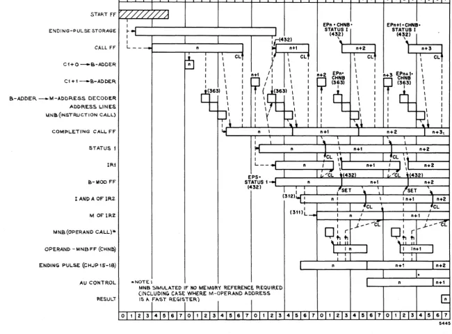
ENDING-PULS~ STORAGE
CALL FF
CHO-B-ADDER
CI + I --B-ADDER
B-ADDER -..M-ADDRESS DECODER
ADDRESS LINES MNa (iNSTRUC.TION CALL)
COMF>LETING CALL. FF
STATUS'
IRf
a-MOD FF
I AND A OF lR2
M 01="1R2
MNB (OPERAND CALL)*"
OPERAND - MNB FF (CHNB)
ENDING PULSE (CHJP IS-18)
AU CONTROL
~ESULT
.. NOTE:
EPS' STATUS 1
(432)
MNB SIMULATED IF NO MEMOR.Y REFERENCe. REQUIR.ED (INCLUDING CASE WHERE M-OPERAND ADDRESS
IS A FAST RE.GISTER)
Figure 2-5. Timing Diagram - Normal Continuous Operation
EPn+I·CHNB· STATUS I
(432) \
n+3 EPn+I' CHNB (363) I
n+2
CL
n
7
(4) FS320 is produced with CT2 which gates instruction n from the mem-ory to IRI.
Performing function (2) produces the address for instruction n
+
1 which is gated to the address lines at t2 of the third cycle by FS363. For this second call, FS363 is generated by gating the outputs of the ending-pulse-storage FF and the status-l FF. This same line which produces FS363 also generates FS432 which, in turn, resets the ending-pulse-storage FF and sets the call FF for n + 1. FS432 also sets the B-mod FF to coincide with the arrival of n in IRI (step 4). As noted on figure 2-4, the output of the B-mod FF is used to control the B-modification process for operand se-lection while also controlling the resetting of the status-l FF for n at to and the clearing of IRI at tl (FS321). It also gates, with CT5, the I and A digits from IRI to IR2 (FS312), and, with CT7, the modified M digits fromthe B-adder to IR2 (FS311).
The setting of the call FF by FS432 again results in setting the
completing-call FF if the MNB signal for n
+
1 is received at t4. Thus the same sequence of events produced by the setting of the completing-call FF is repeated for n + 1. During the time n + 1 is being called and set up in IRl, the ending pulse (CHJP 15, 16, 17, or 18) for n is generated. As noted in figure 2-4, the ending pulse is active during the last 4 micro-seconds of the time that the instruction is being decoded from IR2; that is, during the 4-microsecond period (t6-t5) immediately preceding the last 4 microseconds of instruction execution time in the arithmetic unit. Since we are considering only 4-microsecond instructions at this time, the ending pulse for n is generated during the same interval as I and A of IR2 (figure 2-5).If the operand call to the memory resulting from the B-mod operation is successful, the MNB signal will be present at tl to set the operand-memory-not-busy FF. (Actually there are two operand-MNB FF's which are set at this time; reference heading 3-4.) If no operand memory reference is re-quired, either because of the type of instruction or where the M-operand address specifies a fast register, the MNB signal is simulated to set the operand-MNB FF. The operand-MNB FF stores the operand-call MNB signal for 4 pulsetimes to enable various functions required by the instruction in IR2. Some of these functions are (1) referencing a fast register, (2) stepping the program counter, (3) transmission of instruction information to the AU
(4) various functions of the instruction ending pulse related to the se-quence control of following instructions. The operand-MNB signal together with the ending pulse indicate that the instruction can proceed to the exe-cution phase and therefore the following instructions can advance.
By gating the output of the operand-MNB FF (CHNB) with the instruction ending pulse at t2, the following operations are performed:
(1) Output of B-adder is gated to memory address decoder to make call for instruction n + 2 (FS363).
(2) Call FF is set for n
+
2 if status-l FF is set, indicating n+
1 is in IRI (FS432).(4) I and A of IR2 is cleared of n at t5 (FS3l3).*
(5) M of IR2 is cleared of n at t7 (FS3l4).*
The timing for the execution and result phases of the overall cycle is shown in fi9~re 2-5 simply with two entries: AU control and result.
---. FS3l3 and FS3l4, not shown in figure 2-4, are derived indirectly from the ending pulse
by way of the setting of the progra~counter-clear FF (reference heading 3-5).
SECTION 3
INSTRUCTION SEQUENCE CONTROL
This section contains detailed descriptions- of most conditions of in-struction sequencing. Figure 3-1 t which is referred to throughout this section, is a simplified logic diagram of the normal instruction cycle con-trol circuits. In addition to including everything described in general terms under headings 2-8 and 2-9, figure 3-1 shows how various control sig-nals are generated to take care of different situations which can occur during the normal sequence of operations. Each of the simplified logic diagrams in this manual includes references (D312, D844 , etc.) to the re-lated logic drawing numbers on which can be found the corresponding de-tailed logic.
In this section the principal general areas of control, those asso-ciated with fast register and memory operand references and the program counter, are described first (headings 3-1 through 3-5); special instruc-tion control cases are then described (headings 3-6 through 3-13).
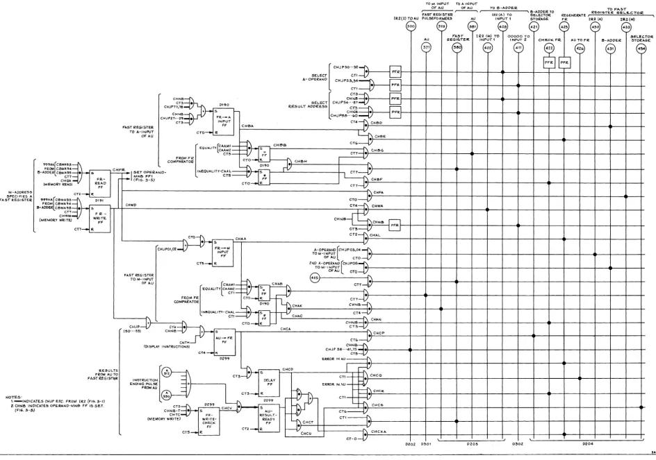
3-1. FAST REGISTER CHAIN CONTROL
The fast register chain control, figure 3-2, contains the logic for controlling the fast register operand (A register) references. These refer-ences include those required to obtain A operands, M operands which specify a fast register, and result storage registers. The control designations and purposes of these three references are:
(1) A-input chain -- selects A operand from normal A operand address (AA) and supplies it to the A-input pulseformers of the AU.
(2) M-input chain -- selects M operand when M address specifies a fast register address (999AA) and supplies it to the M input reg-ister of the AU.
(3) Result chain -- selects A register to store result of instruction and controls transfer of result information from AU to fast reg-ister.
normal A operand to the AU. Data transfer instructions which write infor-mation into the memory use the M-input chaini they also use the result chain when the M address specifies a fast register address. These opera-tions are described under the next two headings but the classification of the instructions involved is described in section 6.
3-2. FAST REGISTER INPUT CHAIN CONTROL
A timing diagram of the A- and M-input chain control operations is given in figure 3-3. This diagram illustrates the repetitive operations for a series of four instructions of minimum length (4 microseconds). The normal A-operand address for instruction n is set up in the fast register selector register by first sending the A part of IR2 to the B-adder'at t2 of the first cycle. This action is produced by FS403 which is generated by instruction control signal CHJP 30. 31, or 32. At the same time, for most instructions, control signal CHJP 33 or 34 causes zeros to enter the other input to the B-adder (FS4ll) so that the sum (A + 0) is equal to the original A-register address (AA). For some instructions different control signals are generated at t2 so that the A-address is modified by adding +1,
+2, or +3 to AA. These cases are needed in double-precision operations for
which an example is given under heading 3-10. Since the extra control sig-nals are not shown in figure 3-2. they are listed below and additional in-formation concerning them is in the Computing Unit Instruction and Function-Signal Analysis manual:
CHJP 35 - +1 to B-adder
CHJP 36 - +2 to B-adder
CHJP 37 - +3 to B-adder
CHJP 77 - +1 or 0 to B-adder
CHJP 78 - +1 or 0 to B-adder
All instructions that require the A-input chain generate control sig-nal CHJP 27. 28, or 29. Either of these sigsig-nals sets the FR-to-A-input FF (signal CHBA) if the operand-MNB FF is set (CHNB). Signal CHNB indicates here that there will be no delay in obtaining the M operand. Signal CHBA
is also produce~ gating CHJP 77 or 78 with the absence of the
operand-MNB-FF signal (CHNB). This is a special case associated with double-precision operations (reference heading 3-10).
, At t4 the contents of the B-adder (A + 0) are read out and transferred to the, fast register selector register by FS431 which is generated by
gating CHBA with CT4. Instruction information for the AU is transferred from the group encoder to the AU at t5 with FS300 which is generated by gating CHJP 38, 39, 40. 41. or 75 with CHNB and CT5.
Signal CHBA is applied to a pair of gates that control the setting of either the equality FF or the inequality FF depending on the results of an A-register comparison test. The details of the comparison test are de-scribed under headings 3-11 and 3-12 dealing with A-register access con-flicts. For the present discussion assume that the inequality FF is set at t6 of the first cycle to produce signal CHBC.
cn
R
START
FF
Dl'l'l (ALSO SI40WN ON FIG . ..,-1)
CNSA
(CAAM 1, 2 ) - - - f \ (EQUALI TV FROM
REG I STEil. COMPARATOR) CT3 CT7
CAAL -....,1---1 (INEQUALITY FROM
REGISTER COMPARATOR)
e-MOD FF D~55 eSSG en CTS eSBS te ~ RESULT)
en
(NONCONTINUOUS, FIG • ..,-n CNEA CH~B
CTO CSSG (e-RESULT)
CNSA
caBA CHJQ-Z
er-t-C~STA~V _ _ _ _ _ _ _ ~
(GEN. CLEAR) EeCL
ECDCS-+-~---~
("10- OVERLAP SWITCH) FIG. 5-1 CQBD
(0 NSF' FIG."'-' LeNBE
CQSA
CTO eS8s (B .. RE!,.ULT) INSTRUCTION INFORMATION
\0 ARITHME1"C UNIT
(All in'itruc.t'o,,'O
MEMORY'~ ~u.iril"'lq Ope1"QM
s R CALL FF Dl'l2 EeeL (G EN. CLEAR) e \ - - - I
CSAA S STATUS-' F'F R CQSA
01 cn
(ALSO S\40WN ON !'IG. 5-')
CT4
CGNB
eOM-(MEMORY PLETING
NOT B!JSV) CALL
FF'
CT4 D~n
eSIW (SET BLOCK-NOT-BUSY FIGURE ~-5
REFERENCE ",.mo., 0 « 0 • • ) C HT 1>., 13, C
10 FIGURE 3-5 GROUP
ENCODER
[ CPeS F IGURE (STEP) 3-9 cpeL (CLEAR)
IIKlTES:
I. _ INDICATES CONTROL SIGN"'L DERIVED FROM INSTRUCTION IN 111.2.
2. CHNB INDIC"'TES OPERAND -MNS IT IS 'OET. (FIGURE 3-5)
3. 0355 ETC. INDICATE'" DETAILED LOGIC DRAWING ~~5!5.
ENDING CHJQ-' ]
PULSES
CHJQ-2,-~ espc.
(TO STAL L FF')
rs-";;'-1--.l-r_ CSPA
CT4 CGee (STA,US -~FF)
FIGURE So,
(DELAYED ENDING PULSE; WIIH eTO, SETS STATUS-3 i'n
CSPS
(ENDING PULSE ,0 ARITHMETIC UNIT)
CSeG (e.REWLT) CT5 CT4 C,' 0'1>55 CSAR S ENDING- CI?_ PULSE-STORAGE FF R caSA
(NO -OVERLAP SWITCH) ECDes
CSCL FF) C,2 eTO e,o CSSG (B" RESULT) eTl en CHJQ-' eT2 CHNS CHJQ-3 (NONCONTINUOUS) CNEA
FI GURE 7-'
(NO- OVERLAP SWITCH)
D~55
csa (A, B, F, L)
e B-,ooDER -IR2IM) 311 MEMORY -111.1 32.0 D2.02 B-AODE!. -MEMORY CLE"'R ADORE"""
Cl DECODER
0301
TO B-ADDER
' - /
D~02.
REGENERI'ITE FAS, \0 FAST REGISTER REGISTER SELECTOR 425 REGISTER
IR'
(r,:-l
ME~6~
I
(e) CLEAR
02.04 O'!l02
ODD-EVEN CHECK, FR
D2.04
5440
TO M INPUT TO A I.JPUT
; OF AU OF AU • r; _ _ "';".O:.,.;:6..;.-,,;.A...:D_0...:E:.R:'::"'_""'I3_ADDER TO FA5T REGISTER [R2 (A) TO SE.CECTOR,
T'l> F","T iRZ(!) TOAU PULSEFORMER5 AU INPUT 1 STORAGe;
RE6ENER"rE r; .:R:,:E:.:o.:,:1,.:: .. ;,,:T,.::E:.:R::...:S::,E=L:,:E.::;C::.."-"TO"'Ia::....---,
FR IR2 (A) Ifi.2(M)
[ , " " , , 0 " • PFR
SELECT cn A-OPERAND CHJP33,34
• PFI< CTI
[ m
<""f>
CT3 • SELECT CHJ P54" CHNI!I '57 • PFF<.CHJPT7,"18 0190 RESULT ADDI<ES5 en
+ 5
f-
CH.JI'> • P'-RCHNB CHJP50"'''0
CHJP27"'2CJ. FR-A
CT4
--r->
CHBDCT:3 INPUT
'-"ST REGISTER FF CHBp" ~
TO A-INPUT CTO_ I<
i~CHBE
OF AU
CT<>
"
EQUALITY CAAM2- • S _
r-+:'I CHI!>G C T 5 - F-F I crr ~ FROM "R "
999;'''[CBWA9:l FROM CBWA94 I3-ADDER ceWA95
en
CHOA (M EMORY ~EAD
-&- .-, - . S
' - FF<.-) - READ
l
~""'--~<"
••
COMPARAToe eTa .. ~ CH6H
1.:\
D190 •
~~
ISET OPeRAND- INEQUALITY-CAO~~
CT7~
MHI!> FF'1 C T 5 . I I
r-
(FlO.. 3-5) GTO _ i F ~CHBF'M-ADDRE55 SPECl FIES A
FAST' 2.EGISTE£ NOTE.S: FF eTZ_ " -999AA[CBWA93
FR.OM ceWA~4
S-ADDER CBWA93 cn
CHWM
(MEMORY WRI TE
-&-
DI~1, - . s -
FF<.-i- WRITE. FF CT7_ R
~ESULT5
FI(:OM AU TO
FAST REGISTER
OM IR2 (FI€>.3-il 1.-INDIC"'TE.S CHJP E.TC. FR
2, CHNI3 INDICATE50PE.I<Aj.JD -WINS FF 15 SET. (FIG. 3-5)
c n
J~CHFA
eTO
CHWD CT4-t\ CHWA
'"".~
CHIIIB• PFR
CT3 CT2--r.). eHAL
~
CHAA ~• 5 CHJP010Z + FF<.-M
v
A-OPE.RAND [CHJP03,04
t INPUT TO M-I NPUT
•
FF OF -,u eTO
C1"5_ I<. 2"'D A-OPERAND [CHJP05
TOM-INPUT • OFAu ero FAST REGISTER
425 ~
TO M-INPUT
CTT~
OF Au
tCAA"'1_~ _~
CHA13 "[~"~'U,_- m~
CTI- FF '::\CT7~
FROM FR CTO R ~
COMPAR-"TOR D190 CHAK CHNB-f
INOQUALITY-CAAL ~TI I : CT4~
•
:,-0-
~
on
<,o:~
'"~
.:\ CHANCHN~~
CHJP CT.f. • CHCA CT3
"
(50"'53) CHN8 + 5
>~CHCP
AU-FR CTI.
CNTH FF
eHNB
(PI5PL"Y INSTRUCTIONS)
CHJP 38'''41,75 •
CT4_ " CT!I
D299 ERR-OR. IN AU
[~~
CT3~
CHCDI
r:-li
5
CT1-
f-W
CHCQI NSTRucnON - DELAV
ERRO~ IN .\U - f- • ENOl"" PULSE - +) FF
FROMAUl~ 5~O I-~CHCR
-V CT3_ I<.
t?
r - + cn 17
0299
'-/---D CHCS
CT~:B- D2~~
• AU- f- •
CHCV 5 •
CHNB-T • 5 C T f . - - - { )
CHTC FR- RE5ULT-
t-CT1~
(MEMORV WI<.ITE)
wRITE-READY ~C ~
CHECK FF • HCT
FF CTZ_ R
CTS_R CHCU )~ CHC)(A
CT-O
300 373 3131 403
FAST Ik!2 1M) TO AU REGISTeR INPUT I
371 seo +02
\ ,
D202 0301 DZO~
421 425 430 +33
00000 TO SELECT
INPUT Z CHECK FR. AU TO FR S-ADDEI< 5TORAG
411 4ZZ 4Z," 431 4S4 PFI< PFR
\ ,
D30Z D204
Figure 3-2. Simplified Logic Diagram - Fast Register Chain
5441
Signal CHSC is gated with the reset output from the equality FF .to pro-duce signal CHBH which, in turn, is gated with CT7 to give FS380. At the same time FS425 is generated by gating CHBA with CT6. (Signal CHBA and CT6 give CHBE which is pulseformed to give FS425 at t7.) FS380 and FS425 then cause the contents of the selected A register to enter the A-input pulse-formers of the AU while also being regenerated in the iast register. (The signal path is shown in the block diagram in figure 2-1.)
By gating CHSC with CT7. signal CHBF is generated to produce FS422 at to. FS422 activates the odd-even check circuits associated with the A-input pulse formers and thereby provides a check on the contents of the fast register. The reason FS422 is dependent on the inequality FF signal is ex-plained under heading 3-12 dealing with A-register access conflicts.
The case where the M address specifies a fast register (999AA) is handled by the fast register M-input chain control logic of figure 3-2. The memory addresses 99901 to 99999 are reserved for the fast registers. Thus. any M address in which the three most significant digits are 999 is detected as a fast register reference. As indicated in figure 3-3, detec-tion is accomplished following the B-modificadetec-tion of the M address at t7 at the output of the B-adder (signals CBWA 93, 94, and 95).
For a fast register M-read operation, the FR-Read FF is set (signal CHFR) by the B-adder signals, a general M-read signal (CHQA. reference
heading 3-4), and CT7. Signal CHFR is then gated wjth CTO to generate FS433 which transfers the two least significant digits (AA) of the modified M address from the M part of IR2 to the fast register selector register. Since no true memory reference is made in this case, signal CHFR produces a simulated operand-MNB signal (CHNB) by setting the operand-MNB FF.
The FR-to-M-input FF is set (signal CHAA) to start the M-input chain control by gating CHFR with CTO. As shown in figure 3-2, this FF may also be set by instruction control signal CHJP 01 or 02 for certain instructions that use the M-input chain for the normal A-operand input to the AU. Also in connection with this feature, control signal CHJP 03 or 04 is gated with CTO to send the A part of IR2 directly to the fast register selector reg-ister (FS430). Another spe~ial control signal is CHJP 05 which, with CTO, sends the contents of the B-adder to the fast register selector register (FS43l). For the particular instructions associated with these operations, refer to the classification of instructions in section 6i also see the Com-puting Unit Instruction and Function-Signal Analysis manual. heading 2-12
(page 31).
Signal CHAA is applied to the setting gates of a second pair of equality-inequality FFts that also depend on the results of an A-register comparison test (headings 3-11 and 3-12). As with the A-input chain assume that the inequality FF is set so that signal CHAC is produced from t2 of the first cycle through to of the second cycle. At t2 signal CHAA is gated with CT2 to produce CHAL which, in turn, is pulseformed to give FS425 at t3. FS425 is then gated with the absence of a CT7 timing signal to give FS380. These two function signals then cause the contents of the selected A reg-ister to enter the A-input pulseformers of the AU while also being regen-erated in the fast registers.
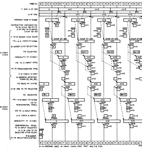
A-INPUT C!-lAIN
M-INPUT C~AIN
TillE (t) 0 I 1 12 I 3 41 516 I 7 0 I 1 I 21 3 4 151 61 7 0 I 1 I 2 I 3 41 5 I 61 7 0 I 1 12 I 3 415 I 81 7
I
n I
,CL
r AND A OF IR2 ... _ _ ...;;..."""T"'_-+...-....,._n;....+;...I...;;..._...-_)+"C"'IL_"""T"'_n;...+...;2...;;...,.I _ _ ...., ,lhC"..L-...--n;....+....;3...;;...~ _ _ ).J.:,C""L--f
lA OF IR2
INSTRUCTION ,NF"ORMATI ON TO AU (C.HJP 38-41,75
A OF IR2 TO B-ADDER
(CI"kIP ~-.32)
o TO B-ADDER (CHVP 33,34)
F"R_ A-INPUT n (CWBAl
B-ADDER TO FR 5ELECTOR
FR SELECTOR
INEOUALITY FF (CHBC)
FR TO A-INPUT PFRs
FR. TO REGENERA"TION ~
O-E CHECI<. ,,-INPOT
M-AOO~E55 DETECTED
(CaWA ~3, 94, 95)
I=R-READ FF (CHFR) n
t!::;n43,,3) M Of: IR2 TO FR 5ELECT()I:\ f-:-I
I=R SELECTOR
n I
I
,_---
CL•
,
n • In+1 I n +2 I n+ 3 I
I CL n+1 I
~ U
n+1
I
--
-I n+2 J
\ (3001
\ 15n+2 (403)\
CL ...--L...,,-i.o..:;i-- -CL
I n+3 I
,
"~) \ U n+3 (403) \\ (4031 \
[!], (4tt) \
I
(4031, n+ID I (411) \ n+ID \ (CHJP 27-29)
n+20\
(41t) I
n + 2 0 '
n+30 \
(4U) "
0
1I ~~) I~
I
n •
~
,1:n
I: "".--n ...
l ~m)
... : ft
"--m(425)
I n
l..
~
"""'(:22)n+1
n+!
r- ..
~)I f-Jn+4 I
l..., I Mn+t!
(CHJP 27-29) n+1 • (-.i(431l
iOn+! I
.. IAn+! I
:
""'~-~-... In+1 •
I
l.. ~)
'.... i ~_n+t
"'--.r:t
' n+t l.. ... ~lf-Jn+1
~ n+2 n+2 J
r- ...
~)I f--I n+2
,
l... IlIn+21
n+30 \ (CHJP 27-29)
n+2 •
~(43t1
: pn+2
I
I. IAn+21 I ' ...
, 'r----,+-...
I • n+2 •
l ~~)
... I L..Jn+2
"'''C:;>
~ n+2'''(~)
...J n+2
~ n+3 n+3 I
~~)
I f--In+3 I
1..., IlIn+31
(CHJP 27-291 n+3
~~
I f-Jn+3
I
10. IAn+31
l
~:(~
'~5
n+3L
n+4L
FR -M-INPlIT FF (O~AAl I~~-:,:,=_'"
FRTO REGENERATION PFR s
n I
i"
I n+1 I
i
I n+2 I I n+3 I
'~"
~.
FR TO A-INPUT Pl'=Rs
O-E CIlECI(, A-INPUT
INEQUAUTY FF (C HAC)
REGENERATION P~RS
TO M-INPUT REGISTER H II 01= IR2 TO ~R.
5EI...ECTOR (CHoIP 03,004) itS-AODER TO FR $ELECT~ (CHIlP 05)
,
,
,
I I I
,
~ • (380) n
~2)
n'~rft
I
,
II I
,
I
,
l.
• L
I
n+1
,
n+2(380)
,
(380)n+4 I
,
n+2 II
Qn+1 I );;In+2
(422)
•
(422) n+1 J L n+2-~~l n+1
ct
n+2*-A-OPERANO USES M- INPUT CHAIN (5EE TElCT AND 1"6.3-2)
I I
I
,
\
,
,
~
I I
Figure 3-3. Timing Diagram - Fast Register Input Chain Control
n+3 (380) n+3 ;;;} n+3 (422) n+3
p~) n+3
CHNB and CT4 to produce FS373 which transfers the contents of the selected A register from the output of the regeneration pulse formers to the M-input register of the AU. The inequality FF signal (CHAC) is also gated directly with CHNB and CT3 to give FS422 at t4. Thust the M-input chain control
transfers information to both the A and M inputs to the AU. The A input is used only to provide the odd-even check on the fast register information. The M-input register then holds the M operand until the normal A operand arrives at the A input at t7.
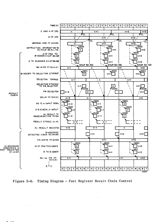
3-3. FAST REGISTER RESULT CHAIN CONTROL
A timing diagram showing several minimum-length instructions passing through the result chain control logic is given in figure 3-4. The fol-lowing discussion, however, is confined to instruction n which can be assumed to be the same 4-microsecond instruction set up in IR2 during the first cycle shown in figure 3-3 for the A-input chain. Following the set-ting of the operand-MNB FF, signal CHNB is gated with control signal CHJP 54, 55, 56, or 57 and CT3, and also with control signal CHJP 58, 59. or 60 and CT3, to produce FS403 and FS411 at t4. These function signals send the A part of IR2 and zeros to the B-adder in order to form the result ad-dress. For double-precision operations the second result address is formed by sending A + 1 to the B-adder at t4 in which the +1 (unit add) is gen-erated by control signal CHJP 61 or 62 (reference heading 3-10).
As shown in figure 3-2t the result chain control is activated by
set-ting the AU-to-FR FF (signal CHCA). This flip-flop is set by gating CHNB with CT4 and result-chain-control-signal CHJP 50, 51, 52. or 53. Signal CHCA is then gated with CT6 to produce FS421 which transfers the result ad-dress from the B-adder to the selector storage. The selector storage holds the address for 4 microseconds (t7 - t6) until it can be transferred to' the fast register selector register. Signal CHCA is gated with CT3 to set the delay FF (CHCD) at t4. The delay FF is needed to store control information until the result of instruction n can be transferred from the AU to the fast register.
Signal CHCD is gated with timing signals and the output of the AU-result-ready FF (CHCU -- set by an instruction ending pulse from AU con-trol) to produce the following control signals to complete the operation:
FS434 (t6) -- transfers contents of selector storage (result address) to fast register selector register.
FS380 (tl) -- reads out old information from selected fast register to A-input pulseformers of AU for check purposes.
FS426 (tl) -- transfers contents of AU result register to fast reg-ister, if no error in AU.
FS422 (t2) -- checks A input of AU to ensure that (1) a fast register was selected and (2) that only one was selected.
RESULT CHAIN
M-AODRES~
SPE;CIFIES A ,AST RE.GISTER
0 ' -.... 0
TIME (t) 0
I ' I
2I
3 4I
~I
.61 7I
0I ' I
2I
3 4I
51 61 7 0I ' I
2I
3 4I
~I
6I
7L AND A OF IR2 /IA OF IRZ
oP£RAND MNB FF (CHNB)
11I5TRueTION INFORMATION TO AU (CJ.lJP :58-4~, 75
AOF IR2 TO e-AOOER (CHJP 5+-57)
o TO S-ADDER (CHJP 58~
AU-FR F, (tHCA)
B-ADDE"R TO SELECTOR STORA.GE
SELECTOR TORAGE
5ELECTOR STORAGE ,0 FR SE.LECTOR
FR SELECTOR
DELAY FF (CoHeo)
FR TO A-INPUT PFRs
O-E CHECK, A-INPUT
AU RESULT TO FlEGENERATION PFRs
R£SUL, STOR"'D IN FI;
I I I I
n I n+' I n+2 I n+3
}JCL /jI'CL }JCL
n / n+1 / n+2/
I.
-
, CL L--
CL L I -CLI n I I n+1 I I n+2 I
:--iir
I n ' - - T I l I n+f: --'ct
I n+2i'-rrr
I n ~~[r I n+f I
~"Lr
n+2 "--EllI n
"'''cf
I n+ti-1j(4ttl
I n.+2
l...
- -,.. (CHJP 50-531 L.. - .... (CHJP ~O-531 l. - ... (CHJP 50-531
n-t I n I n+t I n+2
\
'Ef
\: o t l
\
\ \ n+t \
\
\ \
~I n+2U
n-I I \ n I n+t I
\ \ \ \ \ \ \ \ \ n-I~ m41 (4341
~n-2 \
,'~
\/CP
\
\ ~ n+l~ (4341 \ /n+tD \ ~ n-2tp
(3801 n-2 1- ....I
'i:r
I n-2
l~SI
~n-2
\ - -n-2--L ___ _
n-I ~Ol
kUn-t I ....
·"r:r
In-'
l~SI
L.-J
n-'
\- -n-'---L ___ _
~~Ol
I-. l..!!.J
1 .... ~21
I ~
l-G;JSI
n+t
\--;---
L_r-_-AU RESUL' REGIST£R r--_n_-_2_...II I n-I I n
c
t.Ii-ADDRESS DETECTED (CaWA 9~,9+,95)
F'R-WR1TE n: (cHWo)
M OF IR::! TO B-ADDER
o TO B-ADDER
ETC
~ n+f n+2 n+3[:
n n+t n+2
~TI2)
I n+2
I I-~I
l.. U n+2
.... , ....
r-'fft
I nI-i::f
I I n+'":ffi)
l. n~·D
l., n+t
"-' ... "
n-I I n I n+' I n+2
01'1213 4151S17 01'1213 41 51S17 01'1213 41 5 1S17
5447
Figure 3-4. Timing Diagram - Fast Register Result Chain Control
The result chain is also activated in the case where the M-address specifies a fast register on memory-write (store) instructions (reference heading 3-4 and section 6). Figures 3-2 and 3-4 include the logic and timing for handling this situation. Detection of the M address is accom-plished in the same way as described under the preceding heading for the M-input chain control. In this case the FR-write FF is set (signal CHWD) at to and then gated with CHNB (produced by CHWO) and CT4 to generate FS402 and FS411. These function signals transfer the two least significant digits of the modified M address from the M part of IR2 and zeros to the B-adder to form the result address. Signal CHWO also sets the AU-to-FR FF to start the result chain. The rest of the operations are then carried out as before.
Also shown in figure 3-2 is the FR-write-check FF (signal CHCV) which is used to inhibit the setting of the AU-result-ready FF by the AU ending pulse. This action prevents the operations of the result chain in the case of a memory-write instruction which does not refer to a fast register (in-dicated by signals CHTC and CHNB-T which set the FR-write-check FFj refer-ence heading 3-4). The reason the inhibit is necessary is because all instructions which merely transfer information to or from the memory are handled in the same way in the AU in order to provide for the case where the M address does specify a fast register. Therefore, all such instruc-tions produce the AU ending pulse that sets that AU-result-ready FF.
3-4. OPERAND MEMORY REFERENCE CONTROL
The simplified logic diagram in figure 3-5 shows the basic logic con-cerned with operand memory reference control for all instructions requiring an operand memory reference. Associated timing diagrams are given in fig-ures 3-6 and 3-7. For a memory read operationt the appropriate memory
ref-erence group encoder signals (CLWB'S -- figure 3-1) are buffed together to give memory reference control signals CHTA, CHTB-l, and CHTB-2. The group encoder signals are also gated with the relevant program counter stage sig-nal (CPCR-O for one memory reference or CPCR-l for second memory reference in double-precision operations) to give memory-read signal CHQA. Signal CHRM (and CHQA) is then generated to produce FS363 and FS365 by gating CHQA with CT7. These function signals transfer the modified M address from the B-adder (formed by B-mod operation) to the address lines to make the oper-and call at to. At the same time CHQA generates read signal YBD for mem-ory control purposes.
The operand-MNB signal from the memory (CGNB) is received for instruc-tion n at tl of the second cycle (figures 3-6) to set the operand-MNB FF's. As shown in figure 3-5, there are two operand-MNB FF's which are set by gating CGNB with CHTB-2 and CTl. These flip-flops are designated operand-MNB FFI (signals CHNB 1, 2) and operand-operand-MNB FF2 (signal CHNB-T). Basic-ally, the operand-MNB FF1s are used to remember the receipt of an
[ LWBS INSTRUCTION •
DECODER •
(FIG.3-1) • ETC.
[ CLWB .. INSTRUCTION •
DECODER •
FIG.3-1) •
ETC.
CHJP 13,14 (CHFR
CFI6.3-2)~CHWD
(FI6.3-8) CPCW 01<;'>1
CONDITIONAL TRANSFER ERRORS GEN. CLEAR.
B-MOD.EQUAL
(CSAV, FIG. 3-1)
YBD (READ SIGNI'.L TO MEMORY)
DECODER
~~~~~~~;:;-
]
REI'.D CI'.LL M-I>.DDRESS
~C=H~R~M~.=C~HQ=I>.~ ________________ ~ __________________________________________ - L __ ~~65 DECODER~
CHTA
FF
BLOCK-NOT-BUSY!'"F
D~OO
CTI
CHXA
CGNB CTI
CHTB-2.
OPER.I'.ND-MNB
FFI
D~OO
CT4
CflNB 1,2.
~.L--.... .fSs---l CHNB-T
OPER"'ND-MNB
FF2.
CTI R
ADDRESS LINES
ZEROS---+11 B-ADDER D~02.
.---''----..j402
IR2.(M)---B-ADDER D2.03
REPEAT CALL
CHTB-I CT5
•
+~ ____ ~C~H~T~B~I,~2.~ ________ ~~ ________ ~~=-~ ____ ~ ______ I/ S
Figure 3-5.
CHTC
CHWM
0300
CT3 •
'rBE
(WRITE SIGNAL TO MEMORY)
CTO
DELAY FF2
R.
D202-REGENERI'.TION PFRS -WRITE LINES
,,,
~;~~~" ~,~LT£
B-ADDER.- ]
DECODER-ADDR.ESS LINES 0301
5448
made. Consequently, operand-MNB FFI may also be set by a simulated MNB signal which can be derived in several ways:
(1) By control signals generated for instructions requiring no memory reference (signals CHJP 13, 14)
(2) By signals which indicate that the M-operand address specifies fast register for either memory-read or memory-write instructions
(signals CHFR, CHWD -- reference headings 3-2 and 3-3)
(3) By program-counter-repeat FF signal which steps program counter during long instructions (signal CPCW -- reference heading 3-5).
Operand-MNB FF2 (CHNB-T) is set by a "true" MNB signal only and con-trols several functions of which only two are considered here (reference heading 3-3 and end of this heading). The other functions controlled by CHNB-T are concerned mainly with the details of memory-write instructions which are described in Instruction Sequence Control, Part II.
Heferring to the memory-read operation (figure 3-6), signal CHNB-l is gated with the memory-read control signal (CHTA) and CT4 to set delay FFI at t5. The output from the delay FF is then gated with CT7 to produce FS370 which gates the M operand from the memory read lines into the M-input register of the AU.
If the memory is busy on an operand call, certain other control func-tions must take place in order to repeat the call. The timing of these operations is shown in figure 3-6 where it is assumed that the memory is busy on the first operand call for instruction n
+
1. The call is made at to of the third cycle (FS363, 365) but the MNB signal is not received at tl and operand-MNB FFI is not set. Consequently, the reset output of operand-. MNB FFI (CHNB) is gated with control signal CHTB-l and CT5 to generateFS402 and FS411 which send the M part of IR2 and zeros to the B-adder. The output of the same gate also sets delay FF2 which, with CT7, generates FS311 to gate the B-adder output back to the M part of IR2. Since
instruc-tion n + 1 is retained in IR2, signal CHRM is generated at the same t7 (from CHQA and CT7) which again gives FS363 and FS365. These actions gate the address from the B-adder to the M-address decoder and address lines to repeat the call for instruction n
+
1. (The details of the overall instruc-tion cycle control for this case is given under heading 3-7.)Also shown in figure 3-6 is the case where the M address specifies a
# fast register address (instruction n
+
2). As described previously for theM-input chain control under heading 3-2, the M address is detected at the first t7 after the instruction is set up in IR2 to set the FR-read FF
(signal CHFR, figure 3-2). This signal is then used to set operand-MNB FFI and to start the M-input chain control operations which transfer ,the con-tents of fast register 999AA to the M-input register of the AU.
The timing for a memory-write operation is given in figure 3-7. Many of the functions produced here are similar to those carried out for a
OI)ERAND CALL
OPERAND
REC.EIVE [
REPE.AT
CALL
TIME (t)
r AND A OF IR2.
M OF 1R2.
MEMORY REFE.RENCE CONTROLtHTB-2)
MEMORY' READ (CHRM ,CHQA)
B-ADDER TO M-ADDFIESS D£COOER ADDRESS LINES t.lNB (OPERAND CALL)(C.GNB)
OPERAND-loiNS FFI (CHN6 1,2)
OPEI'\AND- MN6 FF2. ((HNB-l)
MEMORY READ CONTROL ((!-ITA)