VLSI Design of a Variable-Length FFT/IFFT Processor
for OFDM-Based Communication Systems
Jen-Chih Kuo
Graduate Institute of Electronics Engineering and Department of Electrical Engineering, National Taiwan University, Taipei 106, Taiwan
Email:[email protected]
Ching-Hua Wen
Graduate Institute of Electronics Engineering and Department of Electrical Engineering, National Taiwan University, Taipei 106, Taiwan
Email:[email protected]
Chih-Hsiu Lin
Graduate Institute of Electronics Engineering and Department of Electrical Engineering, National Taiwan University, Taipei 106, Taiwan
Email:[email protected]
An-Yeu (Andy) Wu
Graduate Institute of Electronics Engineering and Department of Electrical Engineering, National Taiwan University, Taipei 106, Taiwan
Email:[email protected]
Received 30 January 2003 and in revised form 10 July 2003
The technique of orthogonal frequency division multiplexing (OFDM) is famous for its robustness against frequency-selective fad-ing channel. This technique has been widely used in many wired and wireless communication systems. In general, the fast Fourier transform (FFT) and inverse FFT (IFFT) operations are used as the modulation/demodulation kernel in the OFDM systems, and the sizes of FFT/IFFT operations are varied in different applications of OFDM systems. In this paper, we design and implement a variable-length prototype FFT/IFFT processor to cover different specifications of OFDM applications. The cached-memory FFT architecture is our suggested VLSI system architecture to design the prototype FFT/IFFT processor for the consideration of low-power consumption. We also implement the twiddle factor butterfly processing element (PE) based on the coordinate rotation digital computer (CORDIC) algorithm, which avoids the use of conventional multiplication-and-accumulation unit, but evalu-ates the trigonometric functions using only add-and-shift operations. Finally, we implement a variable-length prototype FFT/IFFT processor with TSMC 0.35µm 1P4M CMOS technology. The simulations results show that the chip can perform (64–2048)-point FFT/IFFT operations up to 80 MHz operating frequency which can meet the speed requirement of most OFDM standards such as WLAN, ADSL, VDSL (256∼2K), DAB, and 2k-mode DVB.
Keywords and phrases:cached FFT, mixed-scaling and rotation CORDIC, and OFDM communications.
1. INTRODUCTION
The orthogonal frequency division multiplexing (OFDM) system is a form of multicarrier modulation (MCM) tech-nologies [1,2,3]. Due to its robustness against frequency-selective fading or narrowband interference, the OFDM technology has been widely implemented in many digi-tal communications such as wireless local area network (WLAN, IEEE 801.11a/g), digital audio/video broadcasting
(DAB/DVB), asymmetric DSL (ADSL), and very-high-speed DSL (VDSL) systems [4,5,6]. The most important mod-ulation/demodulation kernel in OFDM system is the fast Fourier transform and inverse FFT (FFT/IFFT) operations. However, the size and execute time,TFFT, of the FFT/IFFT
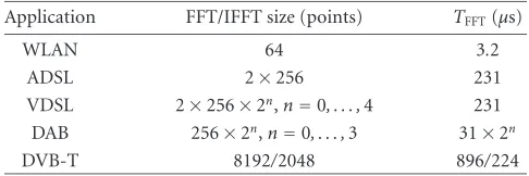
Table1: FFT/IFFT size for OFDM-based communication systems.
Application FFT/IFFT size (points) TFFT(µs)
WLAN 64 3.2
ADSL 2×256 231
VDSL 2×256×2n,n=0, . . . ,4 231 DAB 256×2n,n=0, . . . ,3 31×2n
DVB-T 8192/2048 896/224
224 microseconds for the DAB system. With the preva-lence of multimode/multistandard communication systems, it would be desirable to have a various points of FFT/IFFT processor to fit most OFDM systems.
In this paper, motivated by this trend, we design and implement a variable-length FFT/IFFT processor that can fit various existing OFDM-based communication systems. Firstly, we adopt the newly proposed cached-memory FFT architecture [9] as our suggested VLSI system architecture to lower the main memory access times to reduce the memory power consumption. In addition, we employ mixed-scaling rotation CORDIC (MSR-CORDIC) algorithm [10] to design the butterfly processing element (PE). It can overcome the problems of the long iteration number and large quantiza-tion noise encountered in convenquantiza-tional CORDIC-based PE designs. Besides, this design approach can help to reduce the switching activities, hence to achieve low-power consump-tion in portable communicaconsump-tion applicaconsump-tions. Finally, we de-sign and implement the variable-length prototype FFT/IFFT processor with TSMC 0.35µm 1P4M CMOS technology. The die area of the FFT/IFFT processor is 15.21 mm2 including
2048×32 bits SRAM. The maximum operating frequency can be up to 80 MHz, which can meet most existing OFDM sys-tems using (64–2048)-point FFT/IFFT operations.
The rest of this paper is organized as follows.Section 2
reviews the cached FFT algorithm. We also present our pro-posed system architecture in this section.Section 3discusses the MSR-CORDIC-based PE design.Section 4discusses the design issues of the address generator (AG) and control logic unit (CLU), respectively. Then, inSection 5, we estimate the word length of the FFT hardware architecture. The VLSI im-plementation results and comparisons are made inSection 6. Finally, we conclude this work inSection 7.
2. CACHED FFT ARCHITECTURE 2.1. Review of cached FFT architecture
There are various structures for the implementations of FFT processor, such as single memory, dual memory, pipelined architecture, and array type [9]. Typically, conventional FFT algorithms are developed to minimize the number of multi-plications and additions while maintaining a simple form. However, the hidden memory operations are usually ig-nored. The hidden memory operations might take half of the power consumption of the whole FFT calculation [11]. To reduce the number of memory access, we adopt the
cached-memory architecture [9] to realize the proposed variable-length FFT processor. The cached FFT is designed explicitly to operate on a processor with a hierarchical memory sys-tem. By taking advantage of a small cache memory, the al-gorithm enables higher operating clock frequencies and re-duces data communication energy. On the other hand, most of the memory can operate at lower frequency with only a small portion operates at higher speed. This could reduce the power dissipation.
Figure 1shows the traditional 64-point FFT dataflow di-agram. We can see that the whole data are read and written back to the main memory in every stage. As the FFT size in-creases, stage number will be increased. As a result, the data movement will cause much power consumption and long ex-ecution time.
The basic idea of cached FFT is to reduce the number of main memory access as shown inFigure 2. Instead of pro-cessing one stage of butterfly operation at a time, we store data in local storage and process more data in onesuper-stage (Pass0, Pass1, Pass2)at a period time. To achieve this, two sec-tions of data movement operasec-tions differing from traditional FFT are designed as shown inFigure 3. The resulting opera-tions are still very regular and will not increase much com-plexity. The data will read/write from the cache memory of each super stage. Super stage can greatly reduce the number of main memory access as the FFT sizeNbecomes bigger.
The nomenclature of the cached FFT is defined by fol-lowing stages [9].
(1) Stage.A stage is the part of an FFT where allNmemory locations are read, processed by a butterfly, and written back once.
(2) Super stage.A super stage is the portion of the cached FFT algorithm where allN-data word are loaded into a cache, processed, and written back to the main mem-ory once, which can be regarded as a super stage. (3) Group.A group is the portion of a super stage where
a block of data is read from the main memory into a cached, processed, and written back to the main mem-ory.
(4) Pass.A pass is the portion of a group where each word in the cache is read, processed with a butterfly, and written back to the cache once.
The detailed operations of the cached FFT are as follows.
(1) Input data are loaded into anN-word main memory. (2) The numberCof theNwords is assembled to a group.
TheCwords are loaded into the cache memory. (3) The data in the cache are being processed by PE and
written back to cache. Repeat this step when all passes in a super stage is processed.
(4) Processed data in the cache are flushed to main mem-ory.
(5) Steps 2,3, and 4 are repeated until allN words have been processed once in a super stage.
0 4 8 12 16 20 24 28 32 36 40 44 48 52 56 60
Stage 0 Stage 1 Stage 2 Stage 3 Stage 4 Stage 5
Figure1: Traditional FFT dataflow diagram.
Pass 0 Pass 1 Pass 2 Pass 0 Pass 1 Pass 2 0
4 8 12 16 20 24 28 32 36 40 44 48 52 56 60
Super stage 0 Super stage 1
Figure2: Cached FFT dataflow diagram [9].
PE Cache Memory
Figure3: Cache-memory FFT processor architecture [9].
2.2. Proposed system architecture of the variable-length FFT processor
Based on the design concept of the cached FFT, we propose a variable-length FFT/IFFT processor architecture for OFDM application communication systems. It consists of three de-sign units: CLU, AG, and PE, as shown inFigure 4. The CLU decides the forward/inverse FFT operation and the number of points that FFT will perform, based on the control word. The AG unit can generate the address that RAM and ROM accesses need. With the address, the coefficient ROM can output the twiddle factor to butterfly processing element.
Then the PE can perform the complex arithmetic operations for the data of RAM and the coefficients stored in ROM. The RAM will store the input data as well as the temporary com-puted data and also play the role of the cache. The outputs of the FFT/IFFT results are also stored in the RAM for access. The following sections will discuss the design issues of those major functional units.
3. PROCESSING ELEMENT (PE) DESIGN
C oeffici ent
Figure4: The proposed variable-length FFT/IFFT processor archi-tecture.
processors have employed the CORDIC to perform twiddle factor operations. In this work, we adopted the newly pro-posed MSR-CORDIC scheme [10] to compose these suban-gles. With these easy-to-be-implemented subangles, the ro-tation operations can be performed easily. Besides, the hard-ware requirement of CORDIC is very simple. It also has po-tential advantage of low switching activity for low-power op-erations.
3.1. Review of MSR-CORDIC algorithm
In the conventional CORDIC algorithm [12], the scaling fac-tor is always greater than 1. Therefore, it is necessary to scale down the norm of the input vector to its initial value af-ter the rotation mode is finished. Furthermore, the signal-to-quantization-noise ratio (SQNR) will be reduced due to the growth of the scaling factor. To avoid the overhead of the scaling operation, the product of the scaling factors must be equal to 1. To overcome these problems, the range of the scaling factors must be greater and less than 1. The MSR-CORDIC algorithm [10] reformulates the iterative arith-metic as inAlgorithm 1, whereµi, µj∈ {−1,0,1};IandJ
de-note the number of SPT terms ofx(n) andy(n), respectively, and they are referred to as theextending factors;θnis the ele-mentary angle and the initial value;pn+1denotes the product
of the scaling factors innth iteration. The initial value ofp1
is 1; Nspt are denoted as the number of SPT terms used in
performing (1), which is the sum ofIandJ;Ndenotes the total number of iteration;sn∈ {0,1, . . . , S}andSdenotes the number of maximum shift.
In the conventional CORDIC [12] and EEAS-CORDIC [15] algorithm, the norms of both schemes are enlarged af-ter the micro-rotation operations. That is, the norm is am-plified as illustrated in Figures 5aand5band Rm denotes the total iteration number of CORDIC. On the contrary, in MSR-CORDIC algorithm, (4) shows that the factorPncan be
either greater or less than 1. In Figures5cand5d, we depict the reachable points in 2D plane to emphasize the feature of
Pn.
•Product of the scaling factor
pn+1=pn×pn+1, (5)
End
Algorithm1
FromFigure 5, some other interesting features of the pro-posed scheme are discussed below.
(1) According to (2), the angles in MSR-CORDIC is much denser than the conventional CORDIC and EEAS-CORDIC, hence, the MSR-CORDIC can reach the tar-get angle with fewer iteration as shown inFigure 5d. Furthermore, if we design the parameters,si,µi, ap-propriately so that both the quantization error of ro-tation angles and norms meet the system performance requirement at the same time, then the scaling oper-ation can be avoided. Since we do not need the extra scaling operations, the MSR-CORDIC is faster in com-putational speed and the corresponding hardware cost is reduced.
2 1.5 1 0.5 0 −0.5 −1 −1.5 −2
−2 −1.5 −1 −0.5 0 0.5 1 1.5 2 (a)
1.5 1 0.5 0 −0.5 −1 −1.5 −2
−0.5 0 0.5 1 1.5 2 2.5 3 (b)
2 1.5 1 0.5 0 −0.5 −1 −1.5 −2
−2 −1.5 −1 −0.5 0 0.5 1 1.5 2 (c)
2 1.5 1 0.5 0 −0.5 −1 −1.5 −2
−2 −1.5 −1 −0.5 0 0.5 1 1.5 2 (d)
Figure5: Constellation of reachable points under the rotation process. (a) Conventional CORDIC withN =Rm=4. (b) EEAS-CORDIC with maximum shift rangeS=4 and Rm=2. (c) MSR-CORDIC withI=2,J=1, andN=1. (d) MSR-CORDIC withI=2,J=1, and N =2 for 1/3Pn3 with maximum shift rangeS=4.
3.2. VLSI architecture of MSR-CORDIC for twiddle factor operation
To realize the twiddle factor PE, we use the MSR-CORDIC-based VLSI architecture as shown inFigure 6. In order to en-hance the speed, we arrange two-level pipeline in CORDIC design. The important differences from the conventional CORDIC design are the parameter sequence arrangement, physical consideration, and circuit speedup because of no-scaling operations. Based on (2), both ofx(n+1) andy(n+1) are linear combination of their priorx(n) and y(n). All the coefficients ofx(n) andy(n) are power of two numbers with the signs µi and µj, respectively. Hence, two Barrel shifter
arrays (BSAs) are used to perform shifting operations. The number of the output signal isNsptin each BSA. To perform
the summation of the outputs, 2(Nspt−1) add/subtract
oper-ations must be performed and 2(Nspt−1) adders/subtractors
are used or required to finish the process in one clock cycle. Therefore, in each MSR-CORDIC module, only 2(Nspt−1)
additions/subtractions are required.
3.3. Low switching activity of PE unit
The switching activity of coefficient may cause much power consumption in two’s complement representation system. In CORDIC representation system, the representation of lower switching activity can be achieved. InFigure 7, we can see the different of switching activity between two’s complement and CORDIC representations. The switching activity in CORDIC representation is lower than two’s complement representa-tion.
4. DESIGN OF ADDRESS GENERATOR UNIT AND CONTROL LOGIC UNIT
4.1. Cached FFT/IFFT address generation [9]
For a traditionalradix-r N-point FFT, the stage number is
x(n) y(n)
Barrel shifter array Barrel shifter array
Reg. Reg. Reg. Reg.
ROM and
control unit Reg. Adder/subtrator Reg. Reg. Adder/subtrator
Reg. Reg. Reg. Reg.
Reg. Reg. Adder/subtrator Adder/subtrator
x(n+ 1) y(n+ 1)
Figure6: MSR-CORDIC-(Nspt=3,I=2, andJ=1) based PE structure with two-level pipeline.
two’s complement representation 1 (0000,0000,0001)
−1 (1111,1111,1111)
Rational sequence (µ) of CORDIC 1 (0000,0000,0001)
−1 (1000,0000,0000)
Figure7: Switch activity in two’s complement representation and CORDIC representation.
(1) Group counter:counts the groups of butterflies; (2) Butterfly counter:counts butterfly in a group.
The cached FFT/IFFT address generation circuit can be viewed as a modified version of the traditional FFT. What we need to do is to find a grouping of the memory accesses such that a portion of the full FFT can be calculated using less thanNwords of memory. Fixing the number of bits in the group and butterfly counters, and keeping the positions of the group counter digits fixed across a super stage allows a subset of the FFT to be calculated in memory locations. TheWNcoefficients are generated by using the same method
that the traditional FFT uses, except that the new group and butterfly mappings are used.
Similar to the traditional FFT case, we can map the above derivations into hardware realization by using an outer counter and inner counter. The former responds to the main memory address and the latter is to calculate the cache ad-dress. In any FFT transform, the length (N) and radix (r) must be specified. The cached FFT also requires the
selec-tion of number of super stage (E). So we define some terms, the size N of FFT and the number r of radix-r FFT; the number of passes per groupP = logr(N/E); the cache size
C =rlogrN/E=√EN; the number of groups per super stage,
g =N/C; the number of butterflies per passb=C/r. Then the generalized form of memory and coefficient addresses for cached FFT [9] can be realized with some parameters. In order to perform (64–2048)-point FFT successfully, we choose theradix=2. The radix-2 FFT can perform 64, 128, 256, 512, 1024, and 2048-point operations without any mod-ification in the FFT hardware architecture. However, other radices FFT cannot perform all these points operations. For example, the radix-4 FFT can just perform 64, 256, and 1024-point FFT operations and cannot meet the specification of OFDM applications.Table 2illustrates the address generated by AG for the 64-point radix-2 FFT.
4.2. Variable-length cached FFT/IFFT address generation
Table2: Memory and coefficient addresses for a 64-point,r=2, andE=2 cached FFT.
Super stage (E) Pass Memory address Cache address ROM address
1
0 b5b4b3b2b1b0 b2b1b0 0 0 0 0 0
1 b5b4b3b2b0b1 b2b0b1 b00 0 0 0
2 b5b4b3b0b2b1 b0b2b1 b1b00 0 0
2
0 b2b1b0b5b4b3 b2b1b0 b5b4b30 0
1 b2b0b1b5b4b3 b2b0b1 b0b5b4b30
2 b0b2b1b5b4b3 b0b2b1 b1b0b5b4b3
[000]x[0]
[100]x[4]
[010]x[2]
[110]x[6]
[001]x[1]
[101]x[5]
[011]x[3]
[111]x[7]
W0
N −1
W0
N
−1
W0
N −1
W2
N
−1
W0
N
−1
W0
N −1
W1
N
−1
W0
N
−1
W2
N
−1
W0
N −1
W2
N
−1
W3
N
−1
X[0]
X[1]
X[2]
X[3]
X[4]
X[5]
X[6]
X[7]
(a)
[00]x[0]
[10]x[2]
[01]x[1]
[11]x[3]
W0
N −1
W0
N
−1
W0
N −1
W2
N
−1
X[0]
X[1]
X[2]
X[0]
(b)
Figure8: (a) The generated address in 8-point FFT. (b) The generated address after discarding the LSB in 4-point FFT.
4-point FFT inFigure 8bcan be generated. In the variable-length FFT processor, one addresses that the generator of the 2048-point FFT is necessary. Then we will discard some LSB digits depending on the operating FFT size.
4.3. Control Logic Unit (CLU) design
The topmost CLU is composed of the following individual circuits.
(1) FFT/IFFT operation selection: there is a 1-bit input which determines that the FFT or the IFFT transform should be computed. This will affect the coefficient de-sign and is described inSection 5.
Cache read MSR-CORDIC 1 MSR-CORDIC 2 MSR-CORDIC 3 add/sub Cache write
Figure9: Six-stage cache-PE-cache pipelining scheme.
(3) Data movement:the processing kernel, PE, and cache main memory can operate at different frequency to further reduce the power consumption.
(4) Pipeline of PE: because the state of the FFT proces-sor is independent of datum values, a deeply pipelined FFT processor is much less sensitive to pipeline haz-ards than general-purpose processor. Therefore, the clock speed and throughput rate can be dramati-cally increased with deeper pipelines. We have two-level pipeline, cache-PE-cache, and memory-cache-memory, as discussed below.
Cache-PE-cache pipeline
We have six-stage pipeline as shown inFigure 9. In the first stage, the input operands are read form the appropriate cache set and coefficient from ROM. Stages two to four are the three-stage CORDIC computation. Stage five will calculate the addition/subtract operation. The final stage will write back the result to the cache.
Memory-cache-memory pipeline
The cached FFT architecture significantly reduces the re-quired movement of data to and from the main memory. The main memory arrays can be accessed at low frequency or with idle cycles. The cache is read in the first C stages and the data is written in the main memory. In the second
C stages, the operation is the reverse operations of cache-memory pipeline.
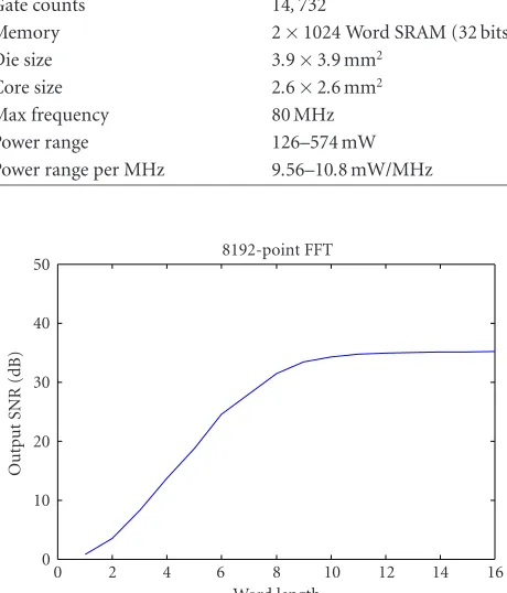
5. FIXED-POINT SIMULATION
The FFT/IFFT processor is designed to perform various lengths of FFT/IFFT operations. For finite word-length def-inition, we have to do fixed-point simulation in the worst case. Based on the specification of OFDM system, the 8192-point FFT will suffer the largest quantization error as it has the most fixed-point calculation. Thus, we will perform sys-tem simulations to decide the finite word length of the hard-ware implementation with 8192-point FFT/IFFT operations. However, there are different channels and specifications for various OFDM applications and the channel models are usu-ally not available. Therefore, we will consider the channel with only additive white Gaussian noise (AWGN). We will also refer to some academic and commercial works to choose parameter to decide the final word length. The simulation environment is shown inFigure 10. The transmitters are usu-ally defined in the standards and have loose requirement than the receivers. Hence, we will only consider the FFT part in the receiver side. First, the signalx(t) passes through the IFFT block and then through the channel with AWGN. The above
IFFT (floating point) Signal
x(t)
Transmitter
Channel AWGN
FFT (fixed point)
Receiver
Figure10: Fixed-point simulation environment.
50
40
30
20
10
0
Output
SNR
(dB)
0 2 4 6 8 10 12 14 16
Word length
SNR=40 dB
SNR=30 dB
SNR=20 dB
SNR=10 dB 8192-point FFT
Figure11: Fixed-point simulation of data word length.
operations have floating point precision. In the receiver side, the receiver signal is cut toB bits and performs the fixed-point FFT calculation.
Table3: Implementation results of the variable-length FFT proces-sor.
Technology TSMC 0.35µm 1P4M CMOS
Voltage 3.3 V
Word length 16 bits Gate counts 14,732
Memory 2×1024 Word SRAM (32 bits) Die size 3.9×3.9 mm2
Core size 2.6×2.6 mm2
Max frequency 80 MHz Power range 126–574 mW Power range per MHz 9.56–10.8 mW/MHz
50
40
30
20
10
0
Output
SNR
(dB)
0 2 4 6 8 10 12 14 16
Word length 8192-point FFT
Figure12: Fixed-point simulation of coefficient word length.
6. IMPLEMENTATION RESULT AND COMPARISON
The prototype FFT/IFFT processor is implemented with TSMC 0.35µm 1P4M CMOS technology. The die area is 3.9×3.9 mm2with 2048-word memory, each is 32 bits wide.
The power normalized by the operating frequency ranges from 9.56 to 10.8 mW/MHz. The microphotograph of the processor is shown inFigure 13.
Table 3 lists the implementation result of this variable-length prototype FFT/IFFT. We can set the operating fre-quency that is based on the execute time of OFDM applica-tions. For example, we have to set the operating frequency to 65 MHz if we want to apply it to the 802.11a WLAN system. The detailed information about the FFT sizes, the respective operating frequency, and the power consumption are listed inTable 4.
In order to eliminate the factor of different fabrication technology, we proposed the normalize index about the chip area and the power consumption. The first normalized in-dex is a normalized area per FFT. Based on this normalized area index, the chip size has to be normalized by the tech-nology process and the FFT size. This area normalized index can evaluate the area requirement per point FFT operation. In this work, we will use normalized area for the FFT design
Core
1Kword SRAM
1Kword SRAM
Figure13: Layout of the FFT/IFFT processor.
based on 0.35µm CMOS technology process to perform fair comparisons. That is,
normalized area per FFT
= Area
(Technology/0.35µm)2·FFT Size×1000.
(6)
In addition, we also proposed the second normalized index about the power consumption, normalized power per FFT. Based on this normalized index, we can consider the effect of the supply voltage, FFT sizes, and operating frequency and then do comparisons with other FFT works very fairly, as follows:
normalized power per FFT
= Power
(Voltage)2·(FFT Size)·Frequency×1000.
(7)
According to these two normalize indexes, we compare the proposed scheme with several existing FFT designs in
Table 5. As we can see, the area requirement and power con-sumption for this work is lower than the works of Baas [9] and Hui et al. [20]. On the other hand, the variable-length FFT/IFFT prototype processor can work at higher operating frequency than the works by Bidet et al. [17] and Jia et al. [21] and can meet various specifications in OFDM applications. It means that we can apply it on the multimode/multistandard OFDM communication systems under the very low imple-mentation cost.
7. CONCLUSIONS
Table4: FFT size,TFFT, frequency, power consumption, and power efficiency.
Application WLAN (IEEE 802.11a) ADSL, VDSL, DAB VDSL, DAB VDSL, DAB, DVB-T
FFT Size (point) 64 512 1024 2048a
TFFT(µs) 3.2 62 128 224
Operating frequency (MHz) 65 12.5 25 60
Power consumption (mW) 545 126 253 574
aSimulated results are based on 4K-word embedded SRAM.
Table5: Comparison of various FFT/IFFT processors.
Processor CMOS tech. (µm) FFT size (points) Freq. (MHz) Area (mm2) Normalized
area per FFT
Normalized
power per FFT Multimode
This Work 0.35 64–2048 60 15.21 7.43 4.67 Yes
Baas [9] 0.6 1024 173 42.88 14.25 4.76 No
Bidet et al. [17] 0.5 8192 20 100 5.98 3.67 No
Colin [20] 0.6 64 36 62.4 331.77 434.03 No
Lihong [21] 0.6 8192 20 140 5.82 3.97 No
then we define the hardware architecture. We also adopted the newly proposed MSR-CORDIC algorithm to improve the rotation number and quantization noise for PE design without scaling operations. Moreover, the PE designs can have the low cost and low power of the advantage. The CLU and AG designs can control the number of points (64–2048) that FFT operations will perform. Finally, the variable-length FFT/IFFT processor is implemented with TSMC 0.35µm CMOS technology process. The chip size is 15.21 mm2and
power consumption ranges between 126–574 mW based on the operating points. The post-layout simulation results show that the variable-length prototype FFT/IFFT can han-dle 64–2048-point OFDM communication systems success-fully.
ACKNOWLEDGMENT
This work was supported in part by the National Science Council, Taiwan, under Grants 2213-E-002-057 and 91-2215-E-002-044.
REFERENCES
[1] I. Kalet, “The multitone channel,” IEEE Trans. Communica-tions, vol. 37, no. 2, pp. 119–124, 1989.
[2] P. Chow, J. C. Tu, and J. M. Cioffi, “Performance evaluation of a multichannel transceiver system for ADSL and VHDSL services,” IEEE Journal on Communications, vol. 9, no. 6, pp. 909–919, 1991.
[3] N. Al-Dhahir and J. M. Cioffi, “Optimum finite-length equal-ization for multicarrier transceivers,” IEEE Trans. Communi-cations, vol. 44, no. 1, pp. 56–64, 1996.
[4] R. V. Paiement, “Evaluation of single carrier and multicar-rier modulation techniques for digital ATV terrestrial broad-casting,” CRC Tech. Rep. CRC-RP-004, Communications Re-search Centre, Ottawa, Ontario, Canada, 1994.
[5] S. Hara, M. Mouri, M. Okada, and N. Morinaga, “Transmis-sion performance analysis of multi-carrier modulation in fre-quency selective fast Rayleigh fading channel,” Wireless Per-sonal Communications, vol. 2, no. 4, pp. 335–356, 1996. [6] ETSI EN 300 401 V1.3.3 (2001-05), “Radio Broadcasting
Sys-tems; Digital Audio Broadcasting (DAB) to mobile, portable and fixed receivers,” 2001.
[7] R. Grisamore, G. N. Rangan, and E. E. Swartzlander Jr., “An efficient FFT processor for ADSL applications,” in Proc. 35th Asilomar Conference on Signals, Systems and Computers, vol. 2, pp. 1251–1255, Pacific Grove, Calif, USA, November 2001.
[8] S. H. Park, D. H. Kim, D. S. Han, K. S. Lee, S. J. Park, and J. R. Choi, “A 2048 complex point FFT processor for DAB systems,” inProc. IEEE International Conference on VLSI and CAD, pp. 309–312, Seoul, Korea, October 1999.
[9] B. M. Baas, “A low-power, high-performance, 1024-point FFT processor,” IEEE Journal of Solid-State Circuit, vol. 34, no. 3, pp. 380–387, 1999.
[10] Z.-X. Lin and A.-Y. Wu, “Mixed-scaling-rotation CORDIC (MSR-CORDIC) algorithm and architecture for scaling-free high-performance rotational operations,” in Proc. IEEE Int. Conf. Acoustics, Speech, Signal Processing, vol. 2, pp. 653– 656, Hong Kong, China, April 2003.
[11] W. Li and L. Wanhammar, “A pipeline FFT processor,” in Proc. IEEE Workshop on Signal Processing Systems, pp. 654– 662, Taiwan, China, October 1999.
[12] Y. H. Hu, “CORDIC-based VLSI architectures for digital sig-nal processing,”IEEE Signal Processing Magazine, vol. 9, no. 3, pp. 16–35, 1992.
[13] A.-Y. Wu and C.-S. Wu, “A unified view for vector rotational CORDIC algorithms and architectures based on angle quan-tization approach,” IEEE Trans. Circuits and Systems, vol. 49, no. 10, pp. 1442–1456, 2002.
[15] C.-S. Wu and A.-Y. Wu, “A novel trellis-based search-ingscheme for EEAS-based CORDIC algorithm,” in Proc. IEEE Int. Conf. Acoustics, Speech, Signal Processing, vol. 2, pp. 1229–1232, Salt Lake City, Utah, USA, May 2001. [16] C.-S. Wu and A.-Y. Wu, “Modified vector rotational CORDIC
(MVR-CORDIC) algorithm and architecture,”IEEE Trans. on Circuits and Systems II: Analog and Digital Signal Processing, vol. 48, no. 6, pp. 548–561, 2001.
[17] E. Bidet, D. Castelain, C. Joanblanq, and P. Senn, “A fast single-chip implementation of 8192 complex point FFT,” IEEE Journal of Solid-State Circuit, vol. 30, no. 3, pp. 300–305, 1995.
[18] H. Shousheng and M. Torkelson, “Designing pipeline FFT processor for OFDM (de)modulation,” inProc. International Symposium on Signals, Systems, and Electronics (ISSSE ’98), pp. 257–262, Pisa, Italy, September–October 1998.
[19] C. H. Chang, C. L. Wang, and Y. T. Chang, “A novel memory-based FFT processor for DMT/OFDM applications,” inProc. IEEE Int. Conf. Acoustics, Speech, Signal Processing, vol. 4, pp. 1921–1924, Phoenix, Ariz, USA, March 1999. [20] C. C. W. Hui, T. J. Ding, J. V. McCanny, and R. F. Woods, “A
new FFT architecture and chip design for motion compensa-tion based on phase correlacompensa-tion,” inProc. International Con-ference on Application-Specific Systems, Architectures, and Pro-cessors, pp. 83–92, Chicago, Ill, USA, August 1996.
[21] L. Jia, Y. Gao, J. Isoaho, and H. Tenhunen, “A new VLSI-oriented FFT algorithm and implementation,” inProc. 11th Annual IEEE International ASIC Conference, pp. 337–341, Rochester, NY, USA, September 1998.
Jen-Chih Kuoreceived the B.S. and M.S. de-grees in electrical engineering from the Na-tional Taiwan University and Graduate In-stitute of Electronics Engineering, Taiwan, in 2000 and 2002, respectively. He is now with Genesys logic, Inc., Taipei, Taiwan. His research interests include VLSI archi-tectures for DSP algorithms, adaptive signal processing, and digital communication sys-tems.
Ching-Hua Wenreceived the B.S. degree in electrical engineering from the National Central University, Taiwan, in 2002. He is now at the Graduate Institute of Electronics Engineering of the National Taiwan Univer-sity. His research interests include VLSI ar-chitectures for DSP algorithms, digital fre-quency synthesizers, and digital communi-cation systems.
Chih-Hsiu Linreceived the B.S. degree in mechanical engineering in 1998 from Na-tional Taiwan University, Taiwan, where he is currently working towards the Ph.D. de-gree in Graduate Institute of Electronics Engineering. His research interests include the VLSI implementation of communica-tion systems and Multiuser deteccommunica-tion for CDMA systems.
An-Yeu (Andy) Wureceived the B.S. degree from National Taiwan University in 1987, and the M.S. and Ph.D. degrees from the University of Maryland, College Park, in 1992 and 1995, respectively, all in electrical engineering. During 1987–1989, he served as a Signal Officer in the Army, Taipei, Tai-wan, for his mandatory military service. From August 1995 to July 1996, he was a member of the technical staffat AT&T Bell