ABSTRACT
MATHUR, SHASHANK. Real -Time Inverter Simulation with Grid Support Capability to meet IEEE 1547 Compliance. (Under the direction of Dr. Subhashish Bhattacharya).
This research focuses on grid connected voltage source inverter and performance
evaluation under test scenarios for grid support functions based on the guidelines specified by
IEEE 1547 grid standard. A real-time simulation environment with Hardware-in-the-loop,
using OPAL RT platform, is designed to emulate real hardware of grid connected system and
the operating characteristics at the PCC interconnection of DER with the Area EPS were
analyzed. There has been a growing interest related to incorporating grid support functions
capability into the DER which is complimented by the most recent advancements in the grid
codes and interconnection standards specifically in new versions of IEEE 1547. OPAL RT is
chosen as the real time simulator for its robust capabilities to model complex power electronic
systems switching at high frequency, model design and test scenarios of power electronic and
power systems under the same platform, and for its rapid adoption as a popular
Hardware-in-the-loop (HIL) technology for system validation, debug and subsystem tests for early design
phase before implementing real hardware thus saving time and cost. Set used is robust, flexible
and re-usable for more advanced testing and evaluations of multiple system configuration,
multi-level topologies and more advanced control functions. The controller hardware can be
validated and after successful run, can be deployed to operate the real hardware. This work can
be used for design, test and validation purposes as a template for interconnection, grid tied
© Copyright 2018 by Shashank Mathur
Real -Time Inverter Simulation with Grid Support Capability to meet IEEE 1547 Compliance
by
Shashank Mathur
A thesis submitted to the Graduate Faculty of North Carolina State University
in partial fulfillment of the requirements for the degree of
Master of Science
Electrical Engineering
Raleigh, North Carolina
2018
APPROVED BY:
_______________________________ _______________________________
Dr. David Lubkeman Dr. Mesut Baran
DEDICATION
To my family for their unconditional love, support and prayers.
To my professors, teachers and mentors for their guidance and inspiration.
BIOGRAPHY
Shashank Mathur was born in Jaipur, India. He received his Bachelor of Technology degree in
Electrical Engineering from Indian Institute of Technology Mandi in May 2014. He started
pursuing Master of Science in Electrical Engineering at North Carolina State University from
August 2015. His research interests in the area of power electronics include DC-AC converters,
DC-DC converters, digital control, grid connected systems, Microgrids, solar photovoltaic
ACKNOWLEDGMENTS
I would like to express my sincere gratitude and regards to my research advisor Dr. Subhashish Bhattacharya for giving me the opportunity to work on recent advancements in the area of grid connected inverters. With his continuous guidance and feedback, I was able to achieve considerable level of conclusion and closure towards the scope of my Master Thesis work. I am grateful for his advice and technical discussions during the entire course of research, and also his constant encouragement despite some hardships on working with some issues and learning the concepts and implementing on the real time simulator platform. Overall, working under his supervision has always inspired me to work harder with the specific goal and focus.
I would also like to convey my sincere thanks to Dr. David Lubkeman and Dr. Mesut Baran for providing me with broader perspective of the problem addressed and their feedback on the work. The discussion I had with my committee members significantly enhanced my knowledge of the subject addressed in this work, and I have been very fortunate to learn a lot from their experience and expertise in this area. Again, I would to thank them sincerely for serving on my thesis committee and with the addition of their guidance, I believe my work would have a better credibility for future use.
My best wishes and thanks to my seniors and project mates Srinivas Gulur, Viju Nair, Dr. Ghanshyamsinh Gohil and Ritwik Chattopadhyay for their guidance and help, especially to Srinivas Gulur from whom I learnt a lot about inverters and controls. I would also like to thank my friends working in other projects at FREEDM Vishnu Mahadeva Iyer, Sayan Acharya, Mahsa Kashani, Heonyoung Kim, Arvind Kumar, Valliappan Muthukaruppan, Thomas Dotson, Rishabh Jain, Keith Dsouza and Qian Long. The valuable suggestions and discussion with my peers have contributed a lot towards my research.
TABLE OF CONTENTS
LIST OF TABLES ... x
LIST OF FIGURES ... xi
LIST OF ABBRVIATIONS ... xv
CHAPTER 1: Introduction and Motivation... 1
1.1. DER – Grid Interconnection ... 1
1.2. Grid Support Functions ... 3
CHAPTER 2: Grid Tied Inverter Design ... 5
2.1. Topology ... 5
2.1.1. Two level voltage source inverter ... 5
2.1.2. Three Level NPC voltage source inverter ... 6
2.2. Phasor Diagram and Power Flow ... 6
2.3. Load Connection: ... 8
2.4. Frame Transformation ... 8
2.5. PLL Design ... 10
CHAPTER 3: Survey of Similar Work ... 16
3.1. Literature Survey ... 16
3.1.1. NREL Report ... 16
3.1.2. UL 1741 SA ... 16
3.1.3. Inverter Controls ... 17
3.2. Focus of this work ... 17
CHAPTER 4: Real-time HIL Simulation Platform ... 18
4.1.1. Subsystem Representation ... 18
4.1.2. Measurement and Parameter Setup ... 18
4.1.3. Grid Emulation in CPU ... 21
4.1.4. Switching Model in FPGA... 22
4.2. Hardware of OPAL RT ... 23
4.2.1. Hardware-in-the-Loop Platform of OPAL RT ... 25
4.2.2. Synchronization and Data Communication ... 26
CHAPTER 5: IEEE 1547 Compliance and Proposed Scheme ... 27
5.1. IEEE 1547 ... 27
5.2. Test Environments and Scenarios ... 27
5.2.1. Voltage and Reactive Power Control ... 29
5.2.2. Voltage and Active Power Control ... 29
5.2.3. Implementation of Control Modes ... 30
5.3. Proposed Scheme ... 31
5.3.1. Controller: ... 32
5.3.2. Algorithm to find load parameters ... 33
5.3.3. Mode Selection based on PLL Output ... 34
5.3.4. Logic Sequence for Controller ... 35
CHAPTER 6: Test Scenarios and Results ... 37
6.1. Case 1: Volt-VAR Control (VVC) when V < 0.92 p.u. ... 37
6.1.1. Inverter currents and PCC voltages ... 37
6.1.2. Results from eHS Scope: ... 39
6.1.2.2. Magnitude of Current vector ... 40
6.1.2.3. PLL Output Vd, Vq ... 41
6.1.2.4. Inverter current in d axis ... 41
6.1.2.5. Inverter Current in q axis ... 42
6.1.2.6. Transition of iq ref (Expanded View) ... 42
6.1.2.7. Active Power P ... 43
6.1.2.8. Reactive Power Q ... 43
6.1.2.9. Apparent Power S ... 44
6.1.2.10. PCC Currents ... 44
6.1.2.11. PCC voltages ... 45
6.1.2.12. Phase variation in currents ... 45
6.1.2.13. Phase variation in voltages ... 46
6.2. Case 2: Volt-VAR Control (VVC) when 0.92 p.u. < V < 0.98 p.u. ... 46
6.2.1. Inverter currents and PCC voltages ... 47
6.2.2. Results from eHS Scope: ... 48
6.2.2.1. Magnitude of voltage vector ... 48
6.2.2.2. Magnitude of current vector ... 49
6.2.2.3. PLL output Vd, Vq ... 49
6.2.2.4. Inverter current in d axis ... 50
6.2.2.5. Inverter current in q axis ... 51
6.2.2.6. Active Power P ... 51
6.2.2.7. Reactive Power Q ... 52
6.2.2.9. PCC currents ... 53
6.2.2.10. PCC voltages ... 53
6.2.2.11. Phase Variation in Currents ... 54
6.2.2.12. Phase Variation in Voltages ... 55
6.3. Case 3: Volt-VAR Control (VVC) when 0.98 p.u. < V < 1.0 p.u. ... 55
6.3.1. Inverter currents and PCC voltages ... 55
6.3.2. Results from eHS Scope: ... 56
6.3.2.1. Magnitude of voltage vector ... 56
6.3.2.2. Magnitude of current vector ... 57
6.3.2.3. PLL output Vd, Vq ... 57
6.3.2.4. Inverter current in d axis ... 58
6.3.2.5. Inverter current in q axis ... 58
6.3.2.6. Active Power P ... 59
6.3.2.7. Reactive Power Q ... 59
6.3.2.8. Apparent Power S ... 60
6.4. Case 4: Volt-VAR Control (VVC) when V > 1.08 p.u. ... 60
6.5. Case 5: Volt-Watt Control (VWC) when 1.07 < V < 1.10 ... 63
6.6. THD (Total harmonic distortion) ... 65
6.6.1. Odd harmonics ... 65
6.6.2. Even harmonics ... 65
CHAPTER 7: Conclusion & Future Work ... 66
7.1. Performance Analysis: ... 66
7.1.1.1. Detection Scheme ... 66
7.1.2. Requirements Covered ... 67
7.1.3. Support Features of Focus ... 67
7.1.3.1. Volt-VAR Control ... 67
7.1.3.2. Volt-Watt Control ... 67
7.2. Conclusion ... 68
7.2.1. Effects of Grid Support ... 68
7.2.1.1. Advantages: ... 68
7.2.1.2. Challenges Faced ... 68
7.2.1.3. Limitations ... 69
7.3. Future Work ... 69
7.3.1. Fault testing and ride thorough cases ... 69
7.3.2. Islanding issues ... 69
7.3.3. Frequency variations ... 69
7.3.4. Expand network to multiple DER and load configuration ... 69
7.3.5. Unbalanced conditions at PCC ... 69
REFERENCES ... 70
LIST OF TABLES
Table 1: Inverter and grid parameters ... 5
Table 2: PLL controller coefficients ... 12
Table 3: Minimum reactive power capability ... 27
Table 4: Q-V Parameters ... 31
Table 5: Set points based on Q-V characteristics ... 31
Table 6: Look up table for controller ... 35
Table 7: Odd harmonics ... 65
LIST OF FIGURES
Figure. 1. PV Inverter with grid integration ... 2
Figure. 2. DER-EPS Interconnection system ... 2
Figure. 3. Local EPS connected to Area EPS ... 3
Figure. 4. Reference diagram for load connection at PCC ... 4
Figure. 5. Two- Level grid connected inverter ... 5
Figure. 6. Three Level NPC grid connected inverter ... 6
Figure. 7. Phasor diagram ... 6
Figure. 8. One line diagram to represent grid connected inverter with load ... 8
Figure. 9. Clarke’s transformation ... 9
Figure. 10. Park’s transformation ... 10
Figure. 11. PLL closed loop control (Phase error)... 11
Figure. 12. PLL closed loop control (Vq error) ... 12
Figure. 13. PLL with transformation blocks ... 12
Figure. 14. PLL controller detailed ... 13
Figure. 15. Per phase equivalent diagram ... 13
Figure. 16. Plant transfer function in d-q plane ... 14
Figure. 17. Current control structure... 14
Figure. 18. id and iq current control loop ... 15
Figure. 19. High Level Subsystem Model on OPAL RT ... 18
Figure. 20. Input Parameters ... 18
Figure. 22. Master Subsystem Block ... 20
Figure. 23. Block diagram of grid model ... 21
Figure. 24. Detailed grid model ... 21
Figure. 25. Two Level Inverter model with grid and load on FPGA ... 22
Figure. 26. Real Time Simulator OPAL RT Hardware ... 23
Figure. 27. I/O port for Analog and Digital signals ... 24
Figure. 28. Tektronix Oscilloscope for DAQ ... 24
Figure. 29. eHS Gen 3 solver ... 25
Figure. 30. Communication port (PCIe port for Optical, LAN port for host) ... 26
Figure. 31. Minimum P-Q capabilities ... 28
Figure. 32. Q-V Characteristics ... 30
Figure. 33. Algorithm for load model parameters ... 34
Figure. 34. Detection Logic ... 36
Figure. 35. Detection of overvoltage and corrective action on set points ... 36
Figure. 36. Case 1: Inverter currents and PCC voltages ... 37
Figure. 37. Case 1: Phase Difference between 3 phase voltage & currents ~ 29 ° ... 38
Figure. 38. Spectrum of different operating points for reactive VPCC support ... 38
Figure. 39. Inverter current (zoomed) increases as reference set point is increased ... 38
Figure. 40. Slower transition of reactive power compensation ... 39
Figure. 41. PCC Voltage Dip ... 40
Figure. 42. Current vector magnitude ... 40
Figure. 44. Inverter Current in d axis ... 41
Figure. 45. Change in q component of inverter current to support grid ... 42
Figure. 46. Zoomed iq showing transition transients ... 42
Figure. 47. Active power transitions ... 43
Figure. 48. Reactive power transitions ... 43
Figure. 49. Apparent power transitions... 44
Figure. 50. Inverter currents transitions ... 44
Figure. 51. PCC Voltage transitions ... 45
Figure. 52. Phase angles of different current vectors in inverter, load and grid branch ... 45
Figure. 53. Phase angles of grid voltage and PCC voltage vectors ... 46
Figure. 54. Case 2: Inverter currents and PCC voltages ... 47
Figure. 55. Case 2: Phase Difference between 3 phase voltage & currents ~ 20 ° ... 47
Figure. 56. PCC Voltage Dip ... 48
Figure. 57. Current vector magnitude ... 49
Figure. 58. Detection of Sag from PLL Output ... 49
Figure. 59. Inverter Current in d axis ... 50
Figure. 60. Change in q component of inverter current to support grid ... 51
Figure. 61. Active power transitions ... 51
Figure. 62. Reactive power transitions ... 52
Figure. 63. Apparent power transitions... 52
Figure. 64. Inverter currents transitions ... 53
Figure. 66. Phase angles of different current vectors in inverter, load and grid branch ... 54
Figure. 67. Phasor representation of currents ... 54
Figure. 68. Phase angles of grid voltage and PCC voltage vectors ... 55
Figure. 69. Case 3: Inverter currents and PCC voltages ... 55
Figure. 70. PCC Voltage Dip ... 56
Figure. 71. Current vector magnitude ... 57
Figure. 72. Detection of Sag from PLL Output ... 57
Figure. 73. Inverter Current in d axis ... 58
Figure. 74. No Change in q component of inverter current ... 58
Figure. 75. Active power transitions ... 59
Figure. 76. Reactive power transitions ... 59
Figure. 77. Apparent power transitions... 60
Figure. 78. Case 4: Phase Difference between 3 phase voltage & currents ~ (-15 °) ... 60
Figure. 79. PCC Voltage rise due to cap load and iq reference current is negative ... 61
Figure. 80. Inverter absorbs reactive power during grid support, PCC voltage reduces ... 62
Figure. 81. Active, Reactive and Apparent power transitions ... 62
Figure. 82. Voltage-active power characteristics ... 63
Figure. 83. Case 5: PLL Voltage change and id ref ... 64
LIST OF ABBRVIATIONS
EPS Electric Power System
DER Distributed Energy Resource
PCC Point of Common Coupling
PV Photo-Voltaic
HIL Hardware-In-the-Loop
MV Medium Voltage
HV High Voltage
SRF Synchronous Reference Frame
PLL Phase Locked Loop
GSF Grid Support Function
MBD Model Based Design
THD Total Harmonic Distortion
SPWM Sine Pulse Width Modulation
NPC Neutral Point Clamped
UPF Unity Power Factor
VVC Volt VAR Control
VWC Volt Watt Control
FWC Frequency Watt Control
DAQ Data Acquisition
MMC Modular Multilevel Converter
CHAPTER 1: Introduction and Motivation
There is an increase in penetration of renewable energy resources (such as PV) to support power generation. Distributed Energy Resources (DERs) are interfaced with the Electric Power System (EPS) through a power electronic converter. This requires for the system to adhere interconnection guidelines specified in IEEE 1547 Std. [4, 5]
Hardware-in-the-loop (HIL) real time simulation is implemented to develop an environment to test controller design and validate physical system with virtual representation of plant model to mimic real hardware offering benefits of cost and practicality, being more flexible to design changes and easier to debug subsystems at an early stage of design.
IEEE 1547 standard (under progress) [5] is intended to be established as a single document of consensus standard technical requirements for DER interconnection providing uniform criteria and guidelines related to operation, test, safety and maintenance of interconnection. It fundamentally covers performance requirements, power capabilities, response to EPS abnormal conditions, power quality and islanding issues [4, 5], among other requirements. This work is an attempt to develop a robust and reusable design and test architecture for interconnection abiding IEEE 1547 guidelines and be used as a foundation template for grid connected systems locally connected to Area EPS.
1.1. DER – Grid Interconnection
Figure. 1. PV Inverter with grid integration
This chapter discusses about motivation of this work and applications of recent advancements in the inverter – grid integration. A control strategy is developed that monitors the parameters at the point of common coupling, and regulates based on the control design. These advancements are rapidly getting adopted by the utilities and recent changes has been discussed in the new drafts of IEEE 1547 standard [4, 5]. Evaluation of the system design and performance modelling using real time simulator provide an early stage validation procedure for the system before testing the hardware and utilize it during initial phases of design and development due to constraint of time, cost, space and resources. The steps followed include system modelling and then implementing hardware in the loop to test the control hardware providing a complete and consistent system level verification and validation procedure of power stage and controller using software and hardware components.
Figure. 2. DER-EPS Interconnection system
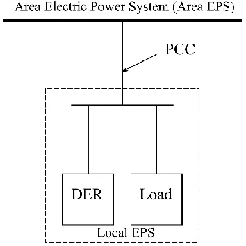
the IEEE 1547 standards incorporating the new control functions. The objective to achieve interconnection requirements [5] along with regulation of PCC voltage while operating in the specified range of operation as specified by the Area EPS.
Figure. 3. Local EPS connected to Area EPS
Three phase loads are common in the industrial applications such as induction motor drive for heavy duty loads which when connected may affect the voltage at the PCC due to sudden demand of power (active and reactive) by the load. These issues are addressed and a control architecture is proposed that would meet some specific requirements of grid support functions.
1.2.Grid Support Functions
Figure. 4. Reference diagram for load connection at PCC
For integration of DER with the Area EPS, there are certain requirements to follow and restrict disturbances at the node of Point of Common Coupling (PCC). Some of these requirements include grid synchronization, voltage and frequency maintenance [4, 5], power quality (allowable under THD limits).
CHAPTER 2: Grid Tied Inverter Design 2.1. Topology
2.1.1. Two level voltage source inverter
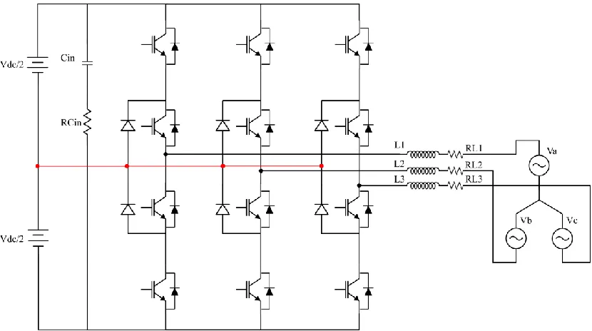
Figure. 5. Two- Level grid connected inverter
Table 1: Inverter and grid parameters.
Parameters
Rated output power 1.7 MVA
Rated AC voltage 4160 V grid voltage (L-L)
Rated frequency 60 Hz
Rated AC current 600 A
Power factor range 0 – 1 (lagging/leading)
Current THD < 5 %
Grid-connected Inverter parameters
Inverter Topology Two Level Voltage source inverter
Switching frequency 10 kHz
DC-link voltage 10 kV
DC-link capacitance Cin = 200uF, R = 0.1 mΩ
Modulation scheme Sine PWM
Harmonic filter L filter
2.1.2. Three Level NPC voltage source inverter
Figure. 6. Three Level NPC grid connected inverter
The maximum current (capacity) can be found based on nameplate rated power. 𝑆 = √3 × 𝑉𝐿−𝐿 (𝑟𝑚𝑠)× 𝐼𝐿(𝑟𝑚𝑠)
1.7 𝑀𝑉𝐴 = √3 × 4160 × 𝐼𝐿(𝑟𝑚𝑠) 𝐼𝐿(𝑟𝑚𝑠) = 235.7 𝐴
𝐼𝐿(𝑝𝑒𝑎𝑘) = 333.3 𝐴
2.2.Phasor Diagram and Power Flow
Φ is used to control active power P and reactive power Q. 𝑃 = 𝑉𝑔𝑟𝑖𝑑 𝜔𝐿 × 𝑉𝑖𝑛𝑣× 𝑆𝑖𝑛𝛷 𝑄 = 𝑉𝑔𝑟𝑖𝑑 𝜔𝐿 × (𝑉𝑖𝑛𝑣𝐶𝑜𝑠𝛷 − 𝑉𝑔𝑟𝑖𝑑) 𝑃𝑜𝑤𝑒𝑟 𝑓𝑎𝑐𝑡𝑜𝑟 = 𝐶𝑜𝑠 𝛷 = 𝑉𝑖𝑛𝑣𝑆𝑖𝑛 𝛷 𝑉𝐿
Vinv is directly related to modulation index m by the following relation:
𝑚 = 𝑉𝑖𝑛𝑣 (𝑉𝐷𝐶 2 )
Note that only half of DC voltage is seen at each node. For unity power factor,
𝑉𝑖𝑛𝑣 = √𝑉𝐿2+ 𝑉𝑔𝑟𝑖𝑑2
𝛷 = tan−1 𝑉𝐿 𝑉𝑔𝑟𝑖𝑑
P and Q calculation are implemented using the following relations:
𝑃 = 𝑣𝑎𝑖𝑎+ 𝑣𝑏𝑖𝑏+ 𝑣𝑐𝑖𝑐
𝑄 = 1
2.3.Load Connection:
Figure. 8. One line diagram to represent grid connected inverter with load
When the load gets connected, we are interested to find out the active, reactive and apparent power flow at the PCC node into the three branches i.e. inverter, load and grid. The power flow equations hold true for this scenario as well, however the analysis is more complex. To simplify the analysis, another approach is followed, as described in later parts pf this chapter. But, before that it is important to understand frame transformation.
2.4.Frame Transformation
The idea behind frame transformation is to represent the three phase quantities into two mutually perpendicular components that both rotate with the grid angular velocity ω, so that from the rotating frame of reference, both appear to be constants. Also, since they are perpendicular, it is easier to de-couple [14] the effects from real and imaginary quantities. These transformation strategies are popularly known as Clarke’s Transformation and Park’s
Figure. 9. Clarke’s transformation
(𝛼𝛽) =
(
1 −1
2 − 1 2 0 √3 2 − √3 2 ) (𝑎𝑏 𝑐)
We represent the 3 phase grid voltage with the following relation taking positive sequence.
𝑉𝑎 = 𝑉𝑚𝑆𝑖𝑛 (𝜔𝑡)
𝑉𝑏= 𝑉𝑚𝑆𝑖𝑛 (𝜔𝑡 − 120°) 𝑉𝑐 = 𝑉𝑚 𝑆𝑖𝑛 (𝜔𝑡 + 120°)
Then,
𝑉𝛼 = 3
2𝑉𝑚𝑆𝑖𝑛 (𝜔𝑡)
𝑉𝛽 = − 3
2𝑉𝑚𝐶𝑜𝑠 (𝜔𝑡)
𝑉 = 𝑉𝛼+ 𝑗 𝑉𝛽
𝑉 = 3
2𝑉𝑚𝑒𝑗(𝜔𝑡−90°)
Clearly, the grid voltage vector V is rotating with time as seen from the, β frame. So, next step is to design a synchronous reference frame (d, q).
Figure. 10. Park’s transformation
(𝑑𝑞) = (𝐶𝑜𝑠 𝜃 𝑆𝑖𝑛 𝜃
𝑆𝑖𝑛 𝜃 − 𝐶𝑜𝑠 𝜃) (
𝛼 𝛽)
2.5.PLL Design
Among the most popular strategies for grid synchronization is Phase Locked Loop [8, 9]. It is a feedback control scheme that automatically adjusts the phase. It is used to synchronize the inverter current angle with the grid phase to reach the power factor close to 1. Inverter phase angle is used to calculate the reference current to be compared with the output current.
The idea is to transform the three phase voltages into two orthogonal voltages in rotating d, q frame. This works using abc to dq transformation block. The idea is to align the voltage vector with one of the d or q component and the other with 0. The PLL structure is an SRF (Synchronous Reference Frame)-PLL [9] and consists of two major parts – phase detection, handled by abc-dq transformation and loop filter that determines the dynamics of the PLL [8, 9]. The bandwidth of the filter will determine the time response to lock the phase and there will be trade off with the filtering action.
Since now we have established the transformation matrices, there is an important step in order for currents to be operating at grid frequency and to minimize the phase error. An SRF-PLL PLL is used for this purpose. The objective is to align vector V with the d axis or d component. This will provide an estimate of the phase angle θ. The d component would provide magnitude and q component provide the information of the phase error between V vector and d axis.
A feedback loop is implemented for the purpose of locking the loop and the dynamics of the controls govern how quickly the voltage vector is able to track the reference d axis. The parameters of the controller [11] would be estimated by comparing the plant transfer function with the fixed coefficients of a PI controller with second order transfer function.
Figure. 12. PLL closed loop control (Vq error)
𝑇(𝑠) = 𝜔𝑛2 + 2𝑄𝜔𝑛𝑠 𝑠2 + 2𝑄𝜔
𝑛𝑠 + 𝜔𝑛2
Here ωn and Q are the natural frequency and damping coefficient respectively for the second order transfer function.
Table 2: PLL controller coefficients.
Vm Q ωn Kp Ki
4160 ×√2
√3 0.707 62.8 rad/s
4 × 𝜔𝑛 × 𝑄
3 × 𝑉𝑚
2 × 𝜔𝑛2
3 × 𝑉𝑚
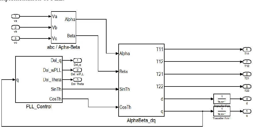
Implementation of PLL:
As depicted in the figure, output of the PLL is Vd and Vq, and also Sin and Cos functions.
Figure. 14. PLL controller detailed
Grid frequency is provided as feedforward to converge faster, however it is not included in the closed loop.
2.6.Closed loop design of current controller
Figure. 15. Per phase equivalent diagram
𝑉𝑖𝑎(𝑡) = 𝐿𝑑𝑖𝑖𝑎
𝑑𝑡 (𝑡) + 𝑅𝑖𝑖𝑎(𝑡) + 𝑉𝑔𝑎(𝑡)
𝑉𝑖𝑏(𝑡) = 𝐿 𝑑𝑖𝑖𝑏
𝑑𝑡 (𝑡) + 𝑅𝑖𝑖𝑏(𝑡) + 𝑉𝑔𝑏(𝑡)
𝑉𝑖𝑐(𝑡) = 𝐿𝑑𝑖𝑖𝑐
𝑑𝑡 (𝑡) + 𝑅𝑖𝑖𝑐(𝑡) + 𝑉𝑔𝑐(𝑡)
When we represent these equation in the d-q frame, we get
𝑉𝑖𝑑= 𝐿𝑑𝑖𝑖𝑑
𝑑𝑡 + 𝑅𝑖𝑖𝑑− 𝜔𝐿𝑖𝑖𝑞 + |𝑉|
It is observed that the d component of voltage has contribution from both id and iq [14], and likewise for q component of voltage.
Figure. 16. Plant transfer function in d-q plane
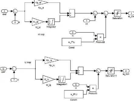
Compensation:
Figure. 17. Current control structure
𝐺𝑐(𝑠) = 𝐿 𝜏+
𝑅 𝜏 𝑠
𝐺𝑐(𝑠) = 𝐾𝑝+ 𝐾𝑖 𝑠
So, Kp = L/ τ ; Ki = R/ τ
So, Kp = 62.84; Ki = 628.32. Here as selected, B.W is 500 Hz.
Implementation of current control loop:
CHAPTER 3: Survey of Similar Work
There has been continued interest in inverter response to abnormal conditions on the grid side. One of the primary area of discussion is grid support capability and how does it affect the dynamics complying with grid codes.
3.1. Literature Survey
3.1.1. NREL Report
Experimental Evaluation of Grid Support Enabled PV Inverter Response to Abnormal Grid Conditions [6]
Analysis in this work included comparative experimental evaluation on four commercially available, three-phase PV inverters, GSF capability and its effect on abnormal grid condition response and impact on run-on times during islanding, peak voltages in overvoltage scenarios, and peak currents during fault events. Some of the functions discussed are voltage ride through, frequency ride through, fixed power factor, volt-var control and frequency watt control. Main focus was on VVC, VWC and FWC control methods and their limitations on run on times.
3.1.2. UL 1741 SA
Small Commercial Inverter Laboratory Evaluations of UL 1741 SA Grid-Support Function Response Times [3]
3.1.3. Inverter Controls
Literature on grid connected inverter and control scheme [7,12,15] has been referred as listed in the references section. Researchers have looked into specific areas of inverter operation and modelling and design related to filter, modulation techniques, controller design, PQ control, etc.
3.2.Focus of this work
This work mainly focusses on the performance of the grid tied inverter for grid support control modes Volt-VAR and Volt-Watt. The objective is to look into the voltage sag and swell cases covering major test scenarios corresponding to the regions of operation in the specific voltage ranges from minimum under voltage to maximum over voltage.
This work proposes a fundamental framework on real time simulation for grid connected switching models with the capability of real time testing and evaluation of control functions. An algorithm for disturbance detection is proposed based on measurement of voltage at the point of common coupling, based on which the reference points for P and Q are set. Another algorithm is designed to calculate the load conditions and parameters required to model inductive or capacitive loads of given rated power demand. This algorithm can also be used for vector analysis of the currents, voltages and impedance parameters within the inverter, load and grid branch and also the nodal analysis at PCC.
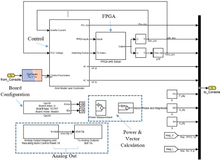
CHAPTER 4: Real-time HIL Simulation Platform 4.1. Software: RT – Lab software interface
4.1.1. Subsystem Representation
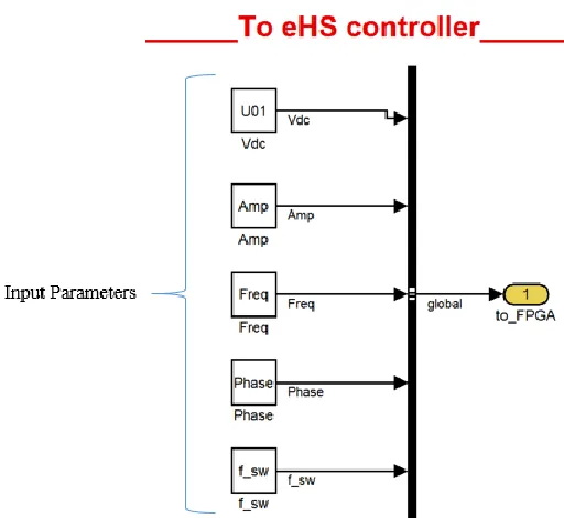
Figure. 19. High Level Subsystem Model on OPAL RT
Figure. 22. Master Subsystem Block
4.1.3. Grid Emulation in CPU
Figure. 23. Block diagram of grid model
The parameters of grid voltage amplitude, frequency and phase that would emulate grid as a 3 phase voltage source is shown in the figure. In the parameters, initial phase angle of phase A is 0 deg and amplitude is set to 4160*sqrt(2/3). The purpose of giving these variables as parameters is not to control them externally during operation, but for design flexibility.
4.1.4. Switching Model in FPGA
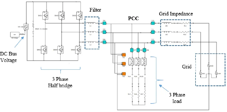
Figure. 25. Two Level Inverter model with grid and load on FPGA
4.2. Hardware of OPAL RT
Figure. 26. Real Time Simulator OPAL RT Hardware
Figure. 27. I/O port for Analog and Digital signals
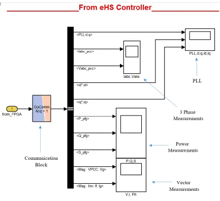
The output from the FPGA, for instance PCC voltage, is sensed as feedback by the CPU using the Analog Out channel, and then based on the controller output, FPGA receives the gate signals from the controller using Digital In channel.
In the figure shown here, there are multiple groups each specified for Analog or Digital data transfer. For synchronization of OP5600 and OP 5607 units, PCIe is used as shown in the figure above.
For purpose of real time measurements, Tektronix TDS 2024C oscilloscope is used with 4 channels and resolution of 2G Sample/ sec at 200 MHz
4.2.1. Hardware-in-the-Loop Platform of OPAL RT
Features include Analog and digital channels on OPAL 5706 (FPGA): 16 Analog In, 32 Analog Out, 128 Digital In and 32 Digital Out ports. eHS Gen3 solver is used to emulate the FPGA model and interface with CPU and is capable of incorporating 72 switching models in a single simulation per eHS. For high order switching models, multiple eHS solver emulating multiple FPGA could be used for applications like MMC using a single core.
Figure. 29. eHS Gen 3 solver
4.2.2. Synchronization and Data Communication
Figure. 30. Communication port (PCIe port for Optical, LAN port for host)
CHAPTER 5: IEEE 1547 Compliance and Proposed Scheme 5.1. IEEE 1547
The series of IEEE 1547 documents are standards for grid integration of Distributed Energy Resource (DER). This standard provides interconnection technical specifications and requirements. It establishes major criteria and requirements for interconnection of distributed resources (DR) with Electric Power System (EPS).It could be used to evaluate performance, operation, testing etc. of the system interconnection. The important node is the point of common coupling.
5.2.Test Environments and Scenarios
Recent changes in IEEE 1547 standards [4,5] provide guidelines for reactive power capability of DER both in terms of injection and absorption. Continuous operation of DER is acceptable provided with grid support during abnormal conditions. For abnormal voltage conditions, reactive power shall be provided subject to DER capacity and is required to be back to normal operation, when voltages become normal. The terminology used when DER injects reactive power is ‘overexcited’ and when DER absorbs reactive power is ‘under-excited’. The amounts of reactive power injection would also depends on the active power output during operation. The DER would inject reactive power only in the case when active power output is at least minimum steady state active power capability, or 5 % of rated power, whichever is greater. For operation greater than the minimum level of active power, the minimum reactive power injection or absorption capability is given in the Table below:
Table 3: Minimum reactive power capability. Injection capability as % of nameplate S
rating (kVA)
Absorption capability as % of nameplate S rating (kVA)
Minimum reactive power requirement [5] is as shown in figure below. It is allowed to curtail active power in order to meet reactive power.
Figure. 31. Minimum P-Q capabilities
5.2.1. Voltage and Reactive Power Control
Before implementation of the control strategies to provide grid support, it is to be noted that the incorporating the control function does not put a requirement for DER to operate at operating points that are outside the minimum capabilities as specified in the table above. However, it is required for DER to have capabilities to provide the following control modes that support reactive power compensation. These modes [5] are activated in a mutually exclusive fashion based on the requirement.
Constant power factor mode (Default: Unity power factor)
Voltage-reactive power (Volt-VAR) mode
Active power-reactive power mode (Watt-VAR)
Constant reactive power mode
5.2.2. Voltage and Active Power Control
This control method provides limitation on maximum active power as a function of voltage. This can be enabled and could remain active when active while the V-Q modes are enabled. Only overvoltage scenarios are dealt using this scheme provided the DER do not absorb real power.
Voltage-active power mode (Volt-Watt)
5.2.3. Implementation of Control Modes
In the subsequent work, the main focus is on Volt-VAR mode. Also, scenarios of operation of Volt-Watt mode is also discussed and implemented.
Volt-VAR mode: This specifies reactive power as a function of voltage. Key guidelines
are:
o DER must follow the piecewise linear Q-V characteristic as shown in figure o These characteristics would be based on the parameters in the table. Please note
that the table provided only mentions the default parameters. However, these parameters are adjustable.
o Open loop response time is 5 s.
Table 4: Q-V Parameters.
V Q
V1 0.92 p.u. Q1 44% of nameplate S rating, injection
V2 0.98 p.u. Q2 0
V3 1.02 p.u. Q3 0
V4 1.08 p.u. Q4 44% of nameplate S rating, absorption
Certain cases are tested to evaluate the control function in the Volt-VAR mode. The points of interest, in general, are in between the boundary condition for each voltage range. Broadly, there are six zones. For generality sake, the names of these zones are kept same as that of the points marked on the figure above, and hence would be called as follows:
Note: VL and VH are low and high set points. For this study these are 0.90 p.u. and 1.10 p.u.
Table 5: Set points based on Q-V characteristics.
Operating Point Zone
Point A VL < V ≤ V1
Point B V1 < V ≤ V2
Point C V2 < V ≤ Vref
Point D Vref ≤ V < V3
Point E V3 ≤ V < V4
Point F V4 ≤ V < VH
5.3.Proposed Scheme
In order to create a test scenario, we require some data on the load that gets connected accidentally that might affect the voltage magnitude. However, this is very uncertain as the PCC voltage is affected by multiple factors and effect of multiple load configuration. Here for the sake of simplicity, we assume just one load getting connected accidentally that affects the voltage to a considerable extent (Amount relative comparable to the p.u. number in the table). For generality sake, and for testing purposes it is a good assumption to model the load using an R-L-C branch. It is intuitive that when the load is predominately inductive (R-L), for e.g. industrial induction motor drive, the PCC would observe a sag in the voltage, whereas, when the load is predominately capacitive (R-C) for e.g. a large capacitor bank, the PCC would observe a swell in the voltage. The amounts of sag and swells would depends on how much reactive power is demanded by the load.
Before looking into the load modelling, let’s divert the attention to compensation schemes. There are two schemes that are proposed. The first utilizes the PLL results to estimate the amount of sag or swell in the PCC voltage and once it is detected, directs the controller to set the new references in order to follow the V-Q characteristics.
The second schemes also assume to have information on the load currents, in addition to the amount of PLL output. Using this extra information, the controller would be able to take a more informed decision of the amount of reactive power to be transacted in order for the voltage compensation. Subsequent sections in this chapter demonstrates the implementation of both the schemes.
5.3.1. Controller:
component of the rotating voltage vector with the grid voltage. Once the two phase angles catch each other, the phase is locked. After this is achieved, then the inverter operation is started by supplying the gate pulses to the power switches in three phase half bridges. This depicts the normal operation of the inverter. After a pre-determined amount of time, the load is connected at the PCC between the inverter and the grid. This create a change in the PCC voltage, depending on sag (inductive load) or swell (capacitive load). Grid codes allow some response time, within which DER is required to take action for the voltage compensation. Keeping this in mind and evaluating the controller dynamic response, another pre-determined setting is activated to update the reference set points in order for Volt-VAR control.
5.3.2. Algorithm to find load parameters
Since, in order for evaluation of inverter performance and purpose of grid compliance, we are simulating some scenarios of disturbance in the PCC voltage, it would not be easy to predict the amount of change in PCC voltage with the given load [16]. This is because, as soon as the load is connected the current vectors change instantaneously and based on the redistributed grid current, the drop across the grid side impedance will determine the change in PCC voltage.
An iterative scheme is developed to determine the affect due the load connection and illustrated as the logic flow as shown below and implemented using an iterative MATLAB C code.
Figure. 33. Algorithm for load model parameters
Based on the Q-V characteristics and Set point table, a look up table is referred. Table 6: Look up table for controller.
Operating Point Values
Point A 0.90 p.u. < V ≤ 0.92 p.u.
Point B 0.92 p.u. < V ≤ 0.98 p.u.
Point C 0.98 p.u. < V ≤ 1.00 p.u.
Point D 1.00 p.u. ≤ V < 1.02 p.u
Point E 1.02 p.u. ≤ V < 1.08 p.u
Point F 1.08 p.u. ≤ V < 1.10 p.u.
5.3.4. Logic Sequence for Controller
The logic block takes input from the detection scheme as the ratio of PLL output and reference voltage. Based on the ratio, the logic looks for the value in the look up table and using the selector switches, takes appropriate action to trigger the change in set point reference of q component of the inverter current. The case shown in the figure depicts the case of overvoltage. Fundamentally, there are three regions of interest, when Vref ≤ V < V3, V3 ≤ V < V4 and V4 ≤ V < VH. Once the region is triggered, there is an instantaneous update as the digital blocks
have very less latency. In this work, the activation time settings is set externally using a step block.
5.3.5. Under-voltage or Over-voltage Detection
Figure. 34. Detection Logic
Value of K is calculated from the following relation:
𝐾 = 0.44
0.06 (0.98 − 𝑉), 𝑢𝑛𝑑𝑒𝑟𝑣𝑜𝑙𝑡𝑎𝑔𝑒 𝑜𝑟 𝐾 = 0.44
0.06 (𝑉 − 1.02), 𝑜𝑣𝑒𝑟𝑣𝑜𝑙𝑡𝑎𝑔𝑒
CHAPTER 6: Test Scenarios and Results
Following tests were conducted to evaluate the performance for grid support Volt-VAR function so as to meet grid code compliance. These tests are studied as different cases based on the level or severity of the disturbance.
6.1. Case 1: Volt-VAR Control (VVC) when V < 0.92 p.u.
The inductive load modelled is of S = 2.6 MVA rating and p.f. 0.3 (L = 13.3 mH, R = 1.57 Ω) The waveforms captured on oscilloscope are scaled down in magnitude. The scaling factor for current and voltages are 0.01x and 0.001x respectively. In addition OPAL RT has an internal attenuation of 0.1 x.
The spikes in PCC voltages are due to the high frequency ripple.
6.1.1. Inverter currents and PCC voltages
Figure. 37. Case 1: Phase Difference between 3 phase voltage & currents ~ 29 °
Figure. 38. Spectrum of different operating points for reactive VPCC support
6.1.2. Results from eHS Scope:
The time stamps for each event in simulation explicitly defined is pre-defined and coded in the control loop after careful consideration of steady state intervals
The time scale is from 0 to 5 s to demonstrate the comparative response of the controller with real time variations (fastest)
The region of operation is depicted as a step function i.e. from inverter to grid connected region instantaneously (worst case). However, it reality the transition would take place within few fundamental cycles. Here a comparison of fast and slow transition is depicted. Fast transition results in overshoot due to bandwidth limitations and imperfect de-coupling of P and Q. The transition can be triggered over a ramp function instead of a step function thus allowing multiple fundamental cycles for the new set points to settle.
Figure. 40. Slower transition of reactive power compensation
It is to be noted that the time intervals are externally set to < 0.5 s, 2 s and > 4s for measurements. These are NOT the response times.
6.1.2.1. Magnitude of voltage vector
Figure. 41. PCC Voltage Dip
6.1.2.2. Magnitude of Current vector
6.1.2.3. PLL Output Vd, Vq
Figure. 43. Detection of Sag from PLL Output
Sag is detected from 5220 V to 4720 V (0.904 p.u.). We inject 44% of Q.
6.1.2.4. Inverter current in d axis
6.1.2.5. Inverter Current in q axis
Figure. 45. Change in q component of inverter current to support grid
This shows that iq reference has now been updated to 220 A (44% of 500 A). The actual q component of inverter current tracks the reference.
6.1.2.6. Transition of iq ref (Expanded View)
Current loop update every quarter cycle and bandwidth decides settling time (20% of 0.01s = 2 ms). From controller bandwidth i.e. 500Hz, it also confirms the settling time of 2 ms.
6.1.2.7. Active Power P
Figure. 47. Active power transitions
6.1.2.9. Apparent Power S
Figure. 49. Apparent power transitions
6.1.2.11. PCC voltages
Figure. 51. PCC Voltage transitions
6.1.2.13. Phase variation in voltages
Figure. 53. Phase angles of grid voltage and PCC voltage vectors
6.2. Case 2: Volt-VAR Control (VVC) when 0.92 p.u. < V < 0.98 p.u.
6.2.1. Inverter currents and PCC voltages
Figure. 54. Case 2: Inverter currents and PCC voltages
6.2.2. Results from eHS Scope:
In this case, the under voltage is detected by the PLL to be 0.94 p.u. Thus, based on the calculation, controller logic would update the set points for Q.
6.2.2.1. Magnitude of voltage vector
6.2.2.2. Magnitude of current vector
Figure. 57. Current vector magnitude
6.2.2.3. PLL output Vd, Vq
From PLL output, we can measure the sag and take necessary action. So, after load gets connected the voltage at PCC is 0.94 p.u. (4875/5220). So, from the sag-swell table, we infer that this operating point is in zone B (0.92 p.u. < V < 0.98 p.u.).
Hence, the controller detects the operating point and calculates the set point of reference. So, Q injection is given by the following relation:
Q =0.44
0.06𝑥 (0.98 − 𝑉)
Q =0.44
0.06𝑥 (0.98 − 0.94)
Q = 29.33 %
6.2.2.4. Inverter current in d axis
6.2.2.5. Inverter current in q axis
Figure. 60. Change in q component of inverter current to support grid
6.2.2.6. Active Power P
6.2.2.7. Reactive Power Q
Figure. 62. Reactive power transitions
6.2.2.8. Apparent Power S
6.2.2.9. PCC currents
Figure. 64. Inverter currents transitions
6.2.2.11. Phase Variation in Currents
Figure. 66. Phase angles of different current vectors in inverter, load and grid branch
Based on the current vectors magnitude and phase analysis, the phasor representation is depicted in the figure below.
6.2.2.12. Phase Variation in Voltages
Figure. 68. Phase angles of grid voltage and PCC voltage vectors
6.3. Case 3: Volt-VAR Control (VVC) when 0.98 p.u. < V < 1.0 p.u.
The inductive load modelled is S = 0.36 MVA rating and p.f. 0.3 (L = 0.13 H, R = 16.15 Ω) The waveforms captured on oscilloscope are scaled down in magnitude. The scaling factor for current and voltages are 0.01x and 0.001x respectively. In addition OPAL RT has an internal attenuation of 0.1 x.
6.3.1. Inverter currents and PCC voltages
6.3.2. Results from eHS Scope:
6.3.2.1. Magnitude of voltage vector
6.3.2.2. Magnitude of current vector
Figure. 71. Current vector magnitude
6.3.2.4. Inverter current in d axis
Figure. 73. Inverter Current in d axis
6.3.2.5. Inverter current in q axis
6.3.2.6. Active Power P
Figure. 75. Active power transitions
6.3.2.7. Reactive Power Q
6.3.2.8. Apparent Power S
Figure. 77. Apparent power transitions
6.4. Case 4: Volt-VAR Control (VVC) when V > 1.08 p.u.
Negative phase represent that current is leading the voltage due to capacitive load
Figure. 80. Inverter absorbs reactive power during grid support, PCC voltage reduces
6.5. Case 5: Volt-Watt Control (VWC) when 1.07 < V < 1.10
Load parameters: (C = 400 uF, R = 2.4 Ω)
V1 =1.07 p.u.; V2 = 1.10 p.u.
P = P rated + Slope*(V- V1) = P = P rated + (-0.8/ 0.03)* (V- 1.07)
6.6. THD (Total harmonic distortion)
According to IEEE 519 standard requirements for THD, the harmonic current injection into the Area EPS at PCC must not exceed the percentages as specified in the table below.
6.6.1. Odd harmonics Table 7: Odd harmonics.
Individual harmonic order h
(odd)
h < 11 11 ≤ h < 17 17 ≤ h < 23 23 ≤ h < 35 35 ≤ h < 50
Total rated current distortion Required
% 4.0 2.0 1.5 0.6 0.3 5.0
Resulted
% 0.187 0.0635 0.0319 0.0326 0.00984 0.507
6.6.2. Even harmonics Table 8: Even harmonics.
Individual harmonic
order h (even) h = 2 h = 4 h = 6
Required % 1.0 2.0 3.0
Resulted % 0.0012 0.0004 0.0027
CHAPTER 7: Conclusion & Future Work 7.1. Performance Analysis:
7.1.1. Response to Disturbances
The response time is a critical parameters to decide the figure of merit of the controller action in events of any abnormal operation condition at the PCC. The detection is an instantaneous action, and only incorporates delays due to processor, followed by reference tracking by the current controller that responds within the range of its bandwidth. As seen in the results section, a typical reference tracking action takes about 2 ms to settle to the reference, which is almost two orders of magnitude less that the maximum response time requirement.
It must be noted that once more complex control function are added, both individual and as combination, the response time would get slower.
7.1.1.1. Detection Scheme
7.1.2. Requirements Covered
The analysis covered major aspects discussed in latest advances in IEEE 1547 in terms of voltage –reactive power control, voltage – active power control, harmonic requirements, set points with adjustable range, combination of control modes as and when specified by the Area EPS and lays the fundamental test ground for evaluating performance in ride through functionality testing, fault detection and response time.
7.1.3. Support Features of Focus
7.1.3.1. Volt-VAR Control
The inverter connected to the grid is tested for a spectrum of major under- voltage and overvoltage points and the results were analyzed to be fairly accurate with the action specified in the IEEE 1547 section of voltage – reactive power control. Also, the seamless detection strategy makes possible a smooth detection over the piecewise linear Q-V characteristics to maintain accurate update of the set point reference. However, this is limited by the sensitivity of the detection logic.
7.1.3.2. Volt-Watt Control
7.2.Conclusion
7.2.1. Effects of Grid Support
It is observed that the control modes have been tested and their performance in terms of providing grid support in occurrences of under voltage or overvoltage, has been demonstrated to be fairly accurate base on the capacity. One concern it that depending on the load, the DER may be insufficient in capacity to bring back the normal operation of the PCC voltage. However, this shows the capability of a DER for a minimum grid support according to requirements from IEE 1547. This can be scaled up to higher percentages to the extent to rated capacity of the DER, while taking other factors into consideration. Also, exploring other mutually exclusive modes of control such as constant power factor mode or the fixed reactive power mode could be a better option to extract full capability for reactive power compensation, however that will be limited in terms of range of operability.
7.2.1.1. Advantages:
Some issues in interconnection of DER with EPS are its capability to inject and absorb reactive power as required by the EPS at the PCC. The test cases have covered the entire range of voltage disturbances at the PCC and evaluated the function of grid support to be able to detect and take action as necessary. Also, this takes advantage of the de-coupled nature of active and reactive components of power, hence regulating voltage function becomes an independent function of active and reactive power as the modes are independently operated. The Volt-VAR and Volt-Watt modes are discussed and implemented using the digital controller. Another major advantage of this scheme is a seamless detection and corrective action as the control algorithm follows a well-defined hierarchy of steps before it changes the reference set points.
7.2.1.2. Challenges Faced
7.2.1.3. Limitations
This methodology comes with some limitation on scope for a more comprehensive architecture, there are other factors that could be incorporated using this template and building on top of this. Some of the issues not covered in this work include cases of unbalanced sag and swell conditions. The PLL design would require little modification for it to not only detect the magnitude of the voltage, but also accurately determine unbalanced condition that would introduce second order harmonics. Also, this scheme takes has indirect control on the power flow at the PCC node using the measurements of three phase quantities which is a critical region for mode errors. This could be improved by introducing a power loop that is slower but could provide more accurate calculations of the new set point of power references I the system. Another limitation is in regard to the range of PCC sag or swell cases. Currently, this work has been focused on cases where the sag or swell is a resultant of a comparable load getting connected. This idea can be extended for fault conditions. Also, detection of islanding and testing anti-islanding scenarios is not covered as part of this work.
7.3. Future Work
7.3.1. Fault testing and ride thorough cases
7.3.2. Islanding issues
Since grid support function are introduced to support the grid during voltage and frequency disturbances, these could also affect islanding detection. It is suggested that anti-islanding methods with grid support would have impacts on run – on times.
7.3.3. Frequency variations
Testing grid support functions for frequency variations under abnormal grid conditions
7.3.4. Expand network to multiple DER and load configuration
7.3.5. Unbalanced conditions at PCC
REFERENCES
[1] Rule 21 Generating Facility Interconnections,” California Public Utility Code, 2000.
[2] Rule No. 14: Service Connections and Facilities on Customer’s Premises,” Hawaiian Electric Company, Inc., Oct. 2015.
[3] S. Gonzalez, J. Johnson, M. J. Reno and T. Zgonena, "Small commercial inverter laboratory evaluations of UL 1741 SA grid-support function response times," 2016 IEEE 43rd Photovoltaic Specialists Conference (PVSC), Portland, OR, 2016, pp. 1790-1795.
[4] D. L. Bassett, "Update of the status of IEEE 1547.8, expanding on IEEE Standard 1547," PES T&D 2012, Orlando, FL, 2012, pp. 1-3.
[5] “IEEE Standard for Interconnection and Interoperability of Distributed Energy Resources with Associated Electric Power Systems Interfaces,” IEEE 1547/D7.0, September 2017.
[6] A. Nelson, G. Martin and J. Hurtt, "Experimental evaluation of grid support enabled PV inverter response to abnormal grid conditions," 2017 IEEE Power & Energy Society
Innovative Smart Grid Technologies Conference (ISGT), Washington, DC, 2017, pp. 1-5.
[7] M. Karimi-Ghartemani, P. Piya, M. Ebrahimi and S. A. Khajehoddin, "A universal controller for grid-connected and autonomous operation of three-phase DC/AC converters," 2015 IEEE Energy Conversion Congress and Exposition (ECCE), Montreal, QC, 2015, pp. 1666-1673.
[9] V. Kaura and V. Blasko, "Operation of a phase locked loop system under distorted utility conditions," in IEEE Transactions on Industry Applications, vol. 33, no. 1, pp. 58-63,
Jan/Feb 1997.
[10] L. P. Sampaio, M. A. G. de Brito, G. de Azevedo e Melo and C. A. Canesin, "Grid-tie three-phase inverter with active and reactive power flow control capability," 2013 Brazilian Power Electronics Conference, Gramado, 2013, pp. 1039-1045.
[11] L. Zhang, L. Harnefors and H. P. Nee, "Power-Synchronization Control of Grid-Connected Voltage-Source Converters," in IEEE Transactions on Power Systems, vol. 25, no. 2, pp. 809-820, May 2010.
[12] G. Wu et al., "Analysis and design of vector control for VSC-HVDC connected to weak grids," in CSEE Journal of Power and Energy Systems, vol. 3, no. 2, pp. 115-124, June 2017.
[13] M. Singh, V. Khadkikar, A. Chandra and R. K. Varma, "Grid Interconnection of Renewable Energy Sources at the Distribution Level With Power-Quality Improvement Features," in IEEE Transactions on Power Delivery, vol. 26, no. 1, pp. 307-315, Jan. 2011.
[14] Arun Karuppaswamy B, “Design and Performance Evaluation of Sub-Systems of Grid-Connected Inverters,” PhD Thesis, July 2014.
[15] K. Arulkumar, K.Palanisamy and D.Vijayakumar, “Recent Advances and Control Techniques in Grid Connected PV System – A Review,” in International Journal of Renewable Energy Research, K.Arulkumar et al., Vol.6, No.3, 2016.
Appendix A
THD of 3 phase grid currents measured from PLECS
Inverter Mode:
Inverter Start THD
Load connected – THD
Grid Support – THD
Individual Harmonic content