ABSTRACT
LONG, JOSEPH PRESTON. Spectroscopic and Electrical Studies of Hafnium-Based High-κ Thin Film Dielectrics on Germanium Surfaces. (Under the direction of Gerald Lucovsky.)
Spectroscopic and Electrical Studies of Hafnium-Based High-κ Thin Film Dielectrics
on Germanium Surfaces
by
Joseph Preston Long
A dissertation submitted to the Graduate Faculty of North Carolina State University
in partial fulfillment of the requirements for the Degree of
Doctor of Philosophy
Physics
Raleigh, North Carolina
2008
APPROVED BY:
________________________ ________________________ Jack Rowe Robert Kolbas
________________________ ________________________ David Aspnes Gerald Lucovsky
Dedication
Biography
Acknowledgements
Table of Contents
LIST OF TABLES ... viii
LIST OF FIGURES ... xi
CHAPTER 1: INTRODUCTION ...1
1.1 – Semiconductor Roadmap ...1
1.2 – Possible Benefits and Drawbacks of Using Germanium Substrates...5
1.3 – High-κ Transition Metal Oxides as Gate Dielectrics on Si...8
1.4 – The Possibility High-κ Transition Metal Oxides on Ge Surfaces...16
1.5 – Overview of the Dissertation ...17
References...29
CHAPTER 2: THIN FILM DEPOSITION AND PROCESSING...34
2.1 – RPECVD Process Overview...34
2.2 – Hafnium-Based High-κ Films by RPECVD ...37
2.3 – Germanium and Germanium-Containing Films by RPECVD...40
2.4 – Thin Film Deposition and Processing: Summary and Conclusions...43
References...50
CHAPTER 3: HAFNIUM BASED HIGH-κ MATERIALS ON GERMANIUM SUBSTRATES ...53
3.1 – Restatement of the Motivation and Proposed Solutions ...53
3.2 – Germanium Substrate Cleaning ...56
3.3 – Sample Preparation ...63
3.4 – Spectroscopic Results for Ge/High-κ Stack Structures ...66
3.5 – Electrical Results for Ge/High-κ Stack Structures...73
3.6 – Summary of Results for High-κ Thin Films on Ge Substrates ...80
References...105
CHAPTER 4: HAFNIUM BASED HIGH-κ MATERIALS ON PSEUDO-MORPHIC GERMANIUM SURFACES GROWN ON SILICON...111
4.1 – Brief Restatement of the Motivation...111
4.2 – Sample Preparation ...111
4.3 – Spectroscopic Properties of Si/PM-Ge/High-κ Structures...115
4.4 – C-V Properties of Si/PM-Ge/High-κ Structures ...118
4.5 – Gate Leakage Properties of Si/PM-Ge/High-κ Structures ...125
References...149
CHAPTER 5: SUMMARY, FUTURE WORK, AND CONCLUDING REMARKS ...152
5.1 – Summary of Experiments and Results...152
5.2 – Recommendations for Future Work...153
5.3 – Concluding Remarks...156
References...158
APPENDIX 161 APPENDIX A: THE THEORY OF POINT GROUPS...162
A.1 – Definition of a Group...162
A.2 – Symmetry Operations ...163
A.3 – Point Groups ...163
A.4 – Representations of Point Groups...165
A.5 – The Reduction of Reducible Representations ...167
A.6 – The Applications of Point Group Theory ...171
References...178
APPENDIX B: MOLECULAR ORBITAL THEORY ...179
B.1 – Molecular Orbitals...179
B.2 – Atomic Orbitals and Their Transformation Properties ...180
B.3 – Bond Hybridization ...182
B.4 – Allowed and Forbidden Transitions ...183
B.5 – Symmetry Adapted Linear Combinations of Atomic Orbitals...186
References...193
APPENDIX C: CRYSTAL FIELD SPLITTING AND JAHN-TELLER DISTORTIONS ...194
C.1 – Crystal Field Splitting ...194
C.2 – Jahn-Teller Distortions...197
References...201
APPENDIX D: THE STRUCTURE AND POLYMORPHISMS OF GROUP IV–B TRANSITION METAL OXIDES AND RELATED ALLOYS...203
D.1 – The Symmetry of Rutile TiO2...203
D.2 – The Symmetry of Baddeleyite ZrO2 and HfO2...208
D.3 – The Symmetry of ([Hf, Ti, Zr]O2)0.3(SiO2)0.3(Si3N4)0.4 Compounds ...213
APPENDIX E: A DESCRIPTION OF INTERMEDIATE PHASES AND
SELF-ORGANIZATION IN NON-CRYSTALLINE SOLIDS ...232
E.1 – Short Range Order: Bond Constraint Theory...232
E.2 – Long Range Order: Intermediate Phases and Percolation Theory ...240
References...251
APPENDIX F: AUGER ELECTRON SPECTROSCOPY (AES) ...252
F.1 – The Auger Process, Auger Electron Detection, and AES Spectra ...252
F.2 – Elemental Analysis by AES...254
F.3 – Thickness Estimations by AES...255
References...262
APPENDIX G: X-RAY ABSORPTION SPECTROSCOPY (XAS)...263
G.1 – The X-Ray Absorption Process and Experiment ...263
G.2 – XAS Spectra...265
References...276
APPENDIX H: SPECTROSCOPIC ELLIPSOMETRY (SE)...278
H.1 – The Theory and Experimental Set-Up for SE...278
H.2 – SE as it Relates to Transition Metal Oxides and Related Alloys...283
References...290
APPENDIX I: MEDIUM ENERGY ION SPECTROSCOPY (MEIS)...291
I.1 – The Theory and Experimental Set-Up for MEIS...291
References...299
APPENDIX J: CAPACITANCE-VOLTAGE (C-V) MEASUREMENTS ...300
J.1 – The Theory of Capacitance in MOS Structures ...300
J.2 – C-V Modeling and the Analysis of MOS Device Structures ...302
References...313
APPENDIX K: CURRENT-VOLTAGE (I-V) MEASUREMENTS...314
K.1 – The Theory of Leakage Current in MOS Structures...314
List of Tables
Chapter 1:
Introduction
NONE
Chapter 2:
Thin Film Deposition and Processing
Table 2.1: The differences between direct and remote plasma CVD processes (after Lucovsky and Tsu [6]). The left side depicts the progression of a direct process; whereas, the
right side depicts the steps in a remote process ...46
Chapter 3:
Hafnium-Based High-
κ
Materials on Germanium
Substrates
Table 3.1: The three germanium chemical surface treatments
investigated using real-time SE and AES ...85 Table 3.2: A summary of the approximate chemical make-up of the
films shown in figure 3.8 ...92
Chapter 4:
Hafnium Based High-
κ
Materials on Pseudomorphic
Germanium Surfaces Grown on Silicon
NONE
Chapter 5:
Summary, Future Work, and Concluding Remarks
Appendix A:
The Theory of Point Groups
Table A.1: The multiplication table for the group C3v. The operation in the left column is applied first, followed by the operation
in the top row ...175 Table A.2: The three irreducible representations for C3v: A1, A2, and E.
A1 and A2 are both one-dimensional, and E is two-dimensional (i.e. a 2 x 2 matrix). Note that all rows and columns of this table are orthogonal as they must be, due to the Great Orthogonality Theorem. (This data can be found
in most texts on point groups, e.g. R. McWeeny [2].)...176 Table A.3: The character table for the group, C3v. Note that table A.3
is simply a compact way of writing the traces of the three representations in table A.2. (This data can be found in most texts on point groups, e.g. R. McWeeny [2] or D.M.
Bishop [3].) ...177
Appendix B:
Molecular Orbital Theory
Table B.1: The symmetry of the atomic orbitals commonly used in
molecular orbital theory...191
Appendix C:
Crystal Field Splitting and Jahn-Teller Distortions
Table C.1: The character table for the cubic point group, Oh...200
Appendix D:
Crystal Field Splitting and Jahn-Teller Distortions
NONE
Appendix E:
The Structure and Polymorphisms of Group IV–B
Transition Metal Oxides and Related Alloys
Appendix F:
The Structure and Polymorphisms of Group IV–B
Transition Metal Oxides and Related Alloys
NONE
Appendix G:
X-Ray Absorption Spectroscopy (XAS)
NONE
Appendix H:
Spectroscopic Ellipsometry (SE)
NONE
Appendix I:
Medium Energy Ion Scattering (MEIS)
NONE
Appendix J:
Capacitance-Voltage (C-V) Measurements
NONE
Appendix K:
Current-Voltage (I-V) Measurements
List of Figures
Chapter 1:
Introduction
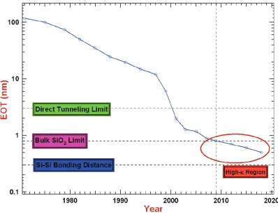
Figure 1.1: Scaling in the EOT for CMOS devices, both historically and as projected by the ITRS (after Wong and Iwai [5]). Note that alternative high-κ dielectrics are now the only
available option for future scaling ...20 Figure 1.2: Measured channel mobilities in silicon CMOS devices
(after Frank, et al. [3] and references therein). Note the decline in mobility for channels with thickness less than
approximately 10 nm ...21 Figure 1.3: A comparison of electron and hole mobilities in both
silicon and germanium (data from refs. [9-12])...22 Figure 1.4: X-ray photoemission spectra showing the thermal
decomposition of GeO2 into gaseous GeO (from Prabhakaran, et al. [15], © 2000 Elsevier Science S.A. All
rights reserved.)...23 Figure 1.5: X-ray photoemission spectra showing the thermal
decomposition of pure Ge3N4 formed by plasma nitridation of the Ge surface. (from Kutsuki, et al. [16], © 2008 The
Japan Society of Applied Physics)...24 Figure 1.6: Core level XPS spectra showing the structure of the
suboxide region at the Si/SiO2 interface on both Si (100) and Si (111) substrates (from Himpsel, et al., © 1988 The
American Physical Society) ...25 Figure 1.7: Cross-section HRTEM micrographs showing the existence
of the ZrSi2 silicide phase in ZrO2/Si interfaces after annealing at 1000ºC (from Stemmer [24], © 2004
American Vacuum Society) ...26 Figure 1.8: The thermal stability of zirconium silicate films as
RTA, (b) an XRD spectrum showing crystallization in a (ZrO2)0.5(SiO2)0.5 film after a 900ºC RTA, and (c) high-resolution TEM micrograph showing chemical phase separation and crystallization in a (ZrO2)0.5(SiO2)0.5 film after a 900ºC RTA (from Rayner, et al., figures 1.8b and 1.8c © 2003 American Vacuum Society). Figures 1.8a and 1.8b show a sharpening of several features at 900ºC, and the circled area of figure 1.8c shows streaking. These signatures all are indicative of crystallinity. The light and dark regions of figure 1.8c show the chemical phase
separation ...27 Figure 1.9: The molecular orbital diagram for oxygen interstitials and
vacancies in various charge states (from Robertson [23], © 2006 IOP Publishing, Ltd.). V0 represents the doubly-occupied neutral vacancy with A1 symmetry. V 0− represents this vacancy with a trapped electron, pulling down an extra state with B1 symmetry from the conduction band. +
0
V represents the singly-occupied vacancy with A1 symmetry. 2+
0
V represents the unoccupied vacancy with A1 symmetry. −
0
I represents the interstitial with a trapped hole. I0 represents the neutral interstitial, which forms an O-O bond and creates a σ* state in the band gap. Lastly, I +0 represents the neutral oxygen interstitial which has formed
an O-O bond and subsequently trapped a hole ...28
Chapter 2:
Thin Film Deposition and Processing
Figure 2.1: A schematic of the RPECVD cluster tool at NCSU used for thin film deposition in these experiments (from Hattangady,
et al. [5], © 1996 American Vacuum Society) ...44 Figure 2.2: A rendering of the gas injection system for the RPECVD
used in these studies. Metal precursor gases are brought in through the gas dispersal rings, and the rest pass through the plasma tube. The sample is held and heated on the
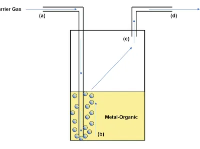
temperature-controlled stage...45 Figure 2.3: The use of solid and liquid metal-organic compounds in
organic compound at point (b), picking up gaseous metal-organic molecules through point (c), and exits to the
deposition chamber at point (d) ...47 Figure 2.4: The metal-organic delivery subsystem constructed for
conducting experiments described in this dissertation. The picture in (a) shows the electronics rack with (listed from bottom to top and left to right): custom valve control switchbox, mass flow controller (MFC) set point controller, upstream pressure gauge, line temperature readout, line temperature zone selector, downstream pressure gauge and controller, pressure gauges power supply, and turbo-molecular pump controller (which never had a home before this). The picture in (b) shows the carrier gas plumbing (top) and (from left to right) the idling pump, variable transformer temperature controls, and constant temperature bath and bubbler (bottom). The figure in (c) is an original
design drawing ...48 Figure 2.5: A schematic diagram of the germane delivery system
(described in the text) for the RPE-MOCVD used in these
experiments ...49
Chapter 3:
Hafnium-Based High-
κ
Materials on Germanium
Substrates
Figure 3.1: Hole mobility enhancement in (a) bulk p-type Ge devices and (b) in Si devices with Si-capped epitaxially grown p -type Ge channels. These devices use either ZrO2 or HfO2
high-κ gate dielectrics (after Saraswat, et al. [4]) ...83 Figure 3.2: XAS spectra showing the nitrogen K1 edge absorption in
plasma-nitrided Ge/HfO2 (top) and Ge/HfSiON (bottom) structures as a function of PDA annealing temperature. (Spectra in each graph are normalized, but not spectra
between graphs.) ...84 Figure 3.3: The imaginary part of the pseudo-dielectric function of
al. method; and the Bare wafer curve corresponds to the as
received substrates ...86 Figure 3.4: Real-time measurements of the evolution of the (a) Ge(111)
and (b) Ge(100) surfaces during two cycles of the NCSU cleaning method (done in collaboration with Seo [36]).
The starting point is after an initial 5 min. H2O bath...87 Figure 3.5: Real-time measurements of the surface re-oxidation on
NCSU-cleaned Ge(100) and Ge(111) surfaces (done in
collaboration with Seo [36]) ...88 Figure 3.6: AES spectra showing the chemical composition of the
native and re-grown Ge(100) overlayers following several of the cleaning methods discussed in the text (done in collaboration with Seo [36]). The wide scan (a) shows the relative concentration of the chemical elements present at the surface, and the narrow scan (b) shows the relative
levels of Ge-O and Ge-Ge bonding at the surface ...89 Figure 3.7: AES spectra showing the chemistry of
RPE-MOCVD-deposited thin films of (a) HfO2 and (b)
(HfO2)0.3(SiO2)0.3(Si3N4)0.4...90 Figure 3.8: MEIS data for HfO2 and (HfO2)0.3(SiO2)0.3(Si3N4)0.4 high-κ
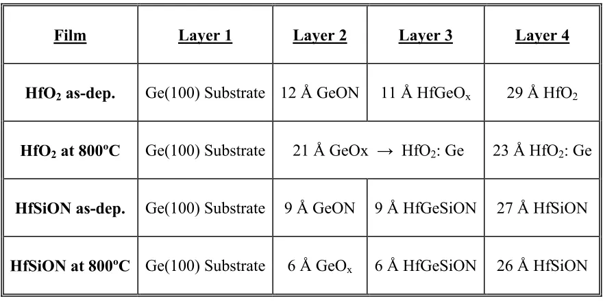
materials deposited on plasma-nitrided Ge(100) substrates. Figures on the left are of HfO2, and figures on the right are of (HfO2)0.3(SiO2)0.3(Si3N4)0.4. Figures on the bottom correspond to as-deposited films, and figures on the top represent the films after RTA at 800ºC. The top of the sample is at 0 nm, with the depth increasing into the sample. The vertical lines are for visual clarity, denoting
transition regions. (Special thanks to K.B. Chung.) ...91 Figure 3.9: Oxygen K1 edge XAS spectra demonstrating the thermal
evolution of HfO2 and (HfO2)0.3(SiO2)0.3(Si3N4)0.4 thin films
deposited on plasma-nitrided Ge(100) and Ge(111) surfaces...93 Figure 3.10: Oxygen K1 edge XAS spectra demonstrating the
asymmetry of HfO2 films deposited on Ge(100) and
Ge(111) substrates and annealed at 800ºC...94 Figure 3.11: The conduction band defect structure for thin films of
annealed at 800ºC as deduced by 2nd derivative XAS. The bandgap assignment for HfO2 is taken from Wong and Iwai [13], and all other energies listed in the band diagrams are
(529.8 eV → 5.7 eV)...95 Figure 3.12: Gaussian fitting of the discrete sub-band edge defect states
in (a) HfO2 and (b) (HfO2)0.3(SiO2)0.3(Si3N4)0.4 thin films (fitting by K.B. Chung). The area of the Gaussian functions for the normalized spectra are plotted as a
function of temperature in (c) ...96 Figure 3.13: The ε2 portion of the dielectric functions for thin films of
HfO2 and HfSiON, both as-deposited and annealed at
800ºC (data taken and analyzed by Seo [36]) ...97 Figure 3.14: (Left) Depth-resolved cathodoluminescence spectra
showing defect level transitions in the bandgap of HfO2 films (CL data is from Brillson, et al. [45], © American Vacuum Society, 2007). (Right) The assigned valence
band defect states consistent with the CL and XAS data...98 Figure 3.15: XAS spectra for plasma nitrided and plasma oxidized Ge
surfaces as compared to plasma-nitrided and plasma
oxidized Si surfaces ...99 Figure 3.16: Relevant band diagrams for the Ge/HfO2 electrical devices
studied in this chapter. Depicted above are (a) flat band conditions for GeO2, Ge3N4, and SiON ITRs, (b) a comparison of substrate injection between GeO2 and SiON ITRs, and (c) a comparison of gate and substrate injection
for the GeO2 ITR...100 Figure 3.17: Typical C-V hysteresis curves for (bottom)
(HfO2)0.3(SiO2)0.3(Si3N4)0.4 and (top) HfO2 gate dielectrics on n-type Ge substrates in these experiments (measurement frequency is 1 MHz). The sweep direction is left-to-right-to
left ...101 Figure 3.18: Typical C-V hysteresis curves for (bottom)
(HfO2)0.3(SiO2)0.3(Si3N4)0.4 and (top) HfO2 gate dielectrics on n-type Ge substrates in these experiments (HfSiON was annealed at 650ºC, and HfO2 was annealed at 600ºC). The
Figure 3.19: Anomalously low leakage current in (HfO2)0.3(SiO2)0.3(Si3N4)0.4-based devices on Ge as a result of high series resistance (top). Evidence of the high series resistance is in the C-V curve (bottom). (Figures are from Lucovsky, et al. [12], © 2008 Elsevier B.V. All rights
reserved.)...103 Figure 3.20: The effects of annealing on the I-V characteristics of the (a)
HfO2 and (b) (HfO2)0.3(SiO2)0.3(Si3N4)0.4 devices studied in this chapter. A Si device is shown in each plot as a reference for comparison. The flat band voltage used is
only approximate as a result of the large C-V hysteresis...104
Chapter 4:
Hafnium Based High-
κ
Materials on Pseudomorphic
Germanium Surfaces Grown on Silicon
Figure 4.1: The evolution of the Si/Ge interface as a function of Ge
deposition time as measured by AES...134 Figure 4.2: The nitrogen K1 edge in Si/Ge/HfO2 samples, both
as-deposited and annealed. The interfacial Ge layer was nitrided before HfO2 deposition. Note that a non-trivial
amount of nitrogen remains after annealing at 700ºC...135 Figure 4.3: XAS spectra showing variations in Si/Ge/high-κ samples
due to substrate orientation, high-κ material, and annealing temperature. Figures (a) on the left depict (HfO2)0.3(SiO2)0.3(Si3N4)0.4 films, and figures (b) on the
right depict HfO2 films...136 Figure 4.4: 2nd derivative XAS spectra showing the conduction band
structures of Si/Ge/high-κ samples and their evolution with post-deposition annealing. The left-hand side depicts (HfO2)0.3(SiO2)0.3(Si3N4)0.4 films, and the right-hand side shows HfO2 films. Note not only the d-state splitting
terms, but the sub-band edge defects as well ...137 Figure 4.5: The energy band structures of the Si/Ge/high-κ samples ...138 Figure 4.6: The C-V characteristics for various Si/PM-Ge/HfSiON
upper left-hand curves are from a Si/HfSiON device
fabricated for reference purposes...139 Figure 4.7: The C-V hysteresis characteristics for various
Si/PM-Ge/HfSiON MOS capacitor structures as a function of interfacial Ge layer thickness. The upper left-hand curve is from a Si/HfSiON device fabricated for reference purposes.
The arrows indicate the sweep directions ...140 Figure 4.8: A summary of the hysteresis, frequency dispersion, fixed
charge density, and interface trap density of the various Si/Ge/HfSiON devices studied in this chapter. The lines shown in the figures are simply cubic splines; they are
meant only as a guide to the eye ...141 Figure 4.9: The 1 MHz C-V characteristics for the thinnest HfSiON
layers deposited. Note the bump near the accumulation
region ...142 Figure 4.10: A plot of measured EOT versus HfSiON deposition time.
Note the non-zero intercept...143 Figure 4.11: A summary of the gate leakage characteristics as a function
of annealing temperature, RPAN time, and Ge deposition time. The leakage curve obtained from a Si/SiO2 device with the same EOT (approximately 3 nm) is shown as a
reference...144 Figure 4.12: Some additional gate leakage I-V curves of interest ...145 Figure 4.13: Gate leakage characteristics for Si/Ge/HfSiON devices with
EOT of approximately 20 Å ...146 Figure 4.14: Best fits to substrate injection data obtained from two
different devices with the Si/Ge/HfSiON device structure. The fits both use a trap-assisted tunneling model, which is a combination of Frenkel-Poole and tunneling leakage
mechanisms...147 Figure 4.15: Several hypothetical band diagrams depicting some of the
GeON, and (d) intentional plasma nitridation of a thin interfacial Ge surface, which unintentionally consumes the entire Ge layer and nitrides the top layer of the Si substrate
as well ...148
Chapter 5:
Summary, Future Work, and Concluding Remarks
NONE
Appendix A:
The Theory of Point Groups
Figure A.1: A pictorial depiction of (a) a counter-clockwise rotation by 90º around the z-axis, (b) a reflection across the plane
normal to the <1, 1, 0> direction, and (c) inversion ...173 Figure A.2: The symmetry of the ammonia molecule...174
Appendix B:
Molecular Orbital Theory
Figure B.1: A representative molecular orbital diagram for a rutile
transition metal oxide (modeled after P.A. Cox [1]) ...192
Appendix C:
Crystal Field Splitting and Jahn-Teller Distortions
NONE
Appendix D:
The Structure and Polymorphisms of Group IV–B
Transition Metal Oxides and Related Alloys
Figure D.1: A schematic representation of (a) the local site symmetry and (b) the atomic orbitals in rutile TiO2. The blue atoms
are titanium, and the green atoms are oxygen...217 Figure D.2: The oxygen K1 x-ray absorption edge spectrum for titanium
Figure D.3: The removal of d-state degeneracy in an octahedral transition metal oxide complex, such as TiO2 (modeled
after Lucovsky, et al. [6])...219 Figure D.4: The idealized 7-fold transition metal local bonding
environment in the baddeleyite structure. The blue atoms
are Zr/Hf, and the green atoms are oxygen...220 Figure D.5: A schematic representation of (a) the local site symmetry
and (b) the hypothetical atomic orbitals in 8-fold coordinated cubic ZrO2 and HfO2. The blue atoms are
Zr/Hf, and the green atoms are oxygen...221 Figure D.6: The oxygen K1 x-ray absorption edge spectrum for hafnium
dioxide (data from Lucovsky, et al. [5]) ...222 Figure D.7: An approximate molecular orbital diagram for the
electronic states of pseudo-cubic hafnia structure having
7-fold coordinated Hf ions ...223 Figure D.8: The removal of d-state degeneracy in a pseudo-cubic,
monoclinic transition metal oxide complex, such as HfO2...224 Figure D.9: The local arrangement of atoms in the idealized structure of
pseudo-ternary (HfO2)0.3(SiO2)0.3(Si3N4)0.4...225 Figure D.10:A schematic representation of (a) the local site symmetry
and (b) the hypothetical oxygen 2p atomic orbitals in the pseudo-ternary, 4-fold coordinated, tetragonal (HfO2)0.3(SiO2)0.3(Si3N4)0.4. The blue atoms are hafnium,
and the green atoms are oxygen...226 Figure D.11:The oxygen K1 x-ray absorption edge spectrum for
pseudo-ternary (HfO2)0.3(SiO2)0.3(Si3N4)0.4 (data from Lucovsky, et
al. [13])...227 Figure D.12:An approximate molecular orbital diagram for the
electronic states of pseudo-ternary, tetragonal (HfO2)0.3(SiO2)0.3(Si3N4)0.4 structure having 4-fold
coordinated Hf ions...228 Figure D.13:The removal of d-state degeneracy in a tetragonal transition
metal oxide complex, such as (HfO2)0.3(SiO2)0.3(Si3N4)0.4
Appendix E:
A Description of Intermediate Phases and
Self-Organization in Non-Crystalline Solids
Figure E.1: A schematic representation of floppy, stressed-rigid, and just-rigid modes in a non-crystalline, covalent network
solid (modeled after Boolchand, et al. [5]) ...245 Figure E.2: The glass forming difficulty in GexSe1-x as a function of
germanium composition, x (from Phillips [1], © 1979
North-Holland Publishing Company) ...246 Figure E.3: Site percolation on the square lattice resistor network
described in the text (modeled after Zallen [7]). The percolation limit, pc, is 0.5 and is one of the few analytic
solutions known in percolation theory...247 Figure E.4: Rigidity in a bond-diluted, generic two-dimensional
network near the percolation limit. Dark regions indicate over-constrained regions, solid lines indicate rigid regions, and open circles indicate floppy regions. (Figure from Jacobs and Thorpe [8], © 1996 The American Physical
Society.) ...248 Figure E.5: The fraction of floppy modes as a function of average
coordination using BCT (solid line) and a computer model for a randomly diluted diamond lattice (dot-dash line). The difference in the onset of rigidity between the two cases indicates an intermediate phase. (From Thorpe, et al. [8],
© 2000 Elsevier Science B.V. All rights reserved.) ...249 Figure E.6: The viscosity (left axis) and reversible heat flow (right
axis) measurements indicating the existence of an intermediate phase in the AsxSe1-x alloy system (after
Boolchand, et al. [9]) ...250
Appendix F:
Auger Electron Spectroscopy (AES)
Figure F.1: The KVV Auger process responsible for electrons detected
in AES experiments discussed in this dissertation...257 Figure F.2: A stereotypical experimental set-up for Auger electron
Figure F.3: Example AES spectra for two different compositions of the pseudo-ternary compound, HfSiON. The elemental AES peak positions are identified, as are the pseudo-ternary compositions computed from the relative atomic
concentrations ...259 Figure F.4: The AES spectra resulting from the incremental oxidation
of a clean Si surface by remote plasma...260 Figure F.5: The oxidation kinetics of a clean Si surface by remote
plasma. This process follows the model for silicon surface oxidation very well, as indicated by the fitting function in
the lower right corner [5, 6] ...261
Appendix G:
X-Ray Absorption Spectroscopy (XAS)
Figure G.1: Representative depictions of the x-ray absorption processes detectable in the TEY: (a) core level excitation into an anti-bonding state, relaxed by Auger electron emission, and (b) core level excitation to the vacuum level (photoelectron emission), relaxed by fluorescent photon emission. Of course, these excitation/relaxation processes do not have to
be paired as they are above ...269 Figure G.2: A schematic representation of beamline 10-1 at SSRL ...270 Figure G.3: Degeneracy removal as a function of electronic state
symmetry as it relates to transition metal compounds
(modeled after Lucovsky, et al. [10])...271 Figure G.4: XAS data showing how d-state degeneracy removal is
observed spectroscopically (data from Lucovsky,
et al. [10])...272 Figure G.5: Complete d-state degeneracy removal in HfO2 as seen in
the 1st derivative XAS spectrum (data from Lucovsky,
et al. [10])...273 Figure G.6: The evolution of the type I crystalline to type II
nano-crystalline transition as observed by XAS in HfO2 on
Figure G.7: The conduction band defect states in a thin film of HfO2 on
Ge(100) as detected by XAS (figure from Seo [11])...275
Appendix H:
Spectroscopic Ellipsometry (SE)
Figure H.1: The experimental set-up for conducting rotating-compensator ellipsometry. The light source is on the left. Variable-frequency incoming light is passed through a polarizer, reflected by the sample, and passed through a rotating compensator and an analyzer. The final intensity
of the beam is measured by the detector ...285 Figure H.2: A non-homogeneous thin film which can be described by
an effective medium theory ...286 Figure H.3: A flow chart representing the method for solving for the
dielectric function of a sample measured by SE ...287 Figure H.4: An example of the absorption constant for a HfO2 sample
as measured by SE. The defect states clearly are identified in this measurement (figure taken from Takeuci, et al. [5],
© 2004 American Vacuum Society)...288 Figure H.5: A representative MO diagram for a transition metal oxide,
such as TiO2, with octahedrally coordinated transition metal atoms and oxygen vacancies. The oxygen vacancies are shown to be within the bandgap at the atomic d state energy. These are the states responsible for the sub-band
edge defect levels observed in figure H.4 ...289
Appendix I:
Medium Energy Ion Scattering (MEIS)
Figure I.1: A schematic representation of the basic ion scattering process in MEIS. In this picture, an ion from the incident
ion beam impacts an atom near the surface of a thin film ...294 Figure I.2: A representative atomic channel for an ion used in
channeling ...295 Figure I.3: The process of scattered ion blocking. The scattered ions
which are not de-channeled essentially are blocked by other
Figure I.4: The experimental set-up for MEIS (top) and ion detection (bottom). (The above figures are from Baumvol [1],
© 1999 Elsevier Science B.V. All rights reserved.) ...297 Figure I.5: An example of depth profiling for a nitrided thin film of
SiO2 on a crystalline Si substrate. The inset shows the depth profile for the ion energy spectrum shown in the main body of the graph. (The figure is taken from Gusev, et al. [6], © 2001 Elsevier Science B.V. All rights
reserved.)...298
Appendix J:
Capacitance-Voltage (C-V) Measurements
Figure J.1: Ideal C-V curves for each of the four possible regions (i.e. accumulation, inversion, depletion, and deep depletion). The C-V curves shown here were computed for an ideal n -type Si MOS structure with a substrate doping level of 1x10¹⁷/cm3, an area of 10µm x 10µm, and an EOT of 10
nm. The device has aluminum contacts ...309 Figure J.2: The effects of interface and oxide trapped charges on the
classical C-V characteristics of a MOS capacitor. The C-V curves shown here were computed for an n-type Si MOS structure with a substrate doping level of 1x10¹⁷/cm3, an area of 10µm x 10µm, and an EOT of 10 nm. The device
has aluminum contacts ...310 Figure J.3: A comparison of the most commonly used capacitance
modeling programs for calculating C-V curves of MOS devices in the ultrathin regime (from Richter, et al. [9],
© 2001 IEEE) ...311 Figure J.4: The effects of series resistance on the capacitance-voltage
characteristics of a MOS device (after Yang and Hu [10]) ...312
Appendix K:
Current-Voltage (I-V) Measurements
emission, (e) thermionic-field emission, (f) trap-assisted
tunneling, and (g) Poole-Frenkel emission ...318 Figure K.2: Direct tunneling and Fowler-Nordeim tunneling in Si/SiO2
MOS devices with varying oxide thickness (data from Schuegraf and Hu [4]). The change in shape of the I-V characteristics shows that the onset of direct tunneling
Chapter 1
Introduction
1.1 – The Semiconductor Roadmap
The International Technology Roadmap for Semiconductors (ITRS) is an
international panel, containing experts from Europe, Taiwan, Korea, Japan, and the US,
whose mission is to perpetuate the various advancement trends in the semiconductor
industry. The ITRS addresses all aspects of the industry, from device design and
manufacture, to device reliability and testing, to the development of new materials. Since
many of these developments are coupled, the ITRS regularly examines the areas in which
progress is being made and those in which more work is needed, constantly creating and
revising relevant benchmarks and timelines to ensure that the industry as a whole
advances [1].
One of the most famous trends addressed by the ITRS is device scaling, known as
Moore’s Law. In 1965, Gordon Moore stated that the number of bits available for
memory on integrated circuits (ICs) would double every year, and that trend has
continued, remarkably, for decades since [2]. In their present form, the basic idea behind
device scaling is to make memory elements smaller by a factor, α, and to increase the
electric fields within devices by a factor, ε, without sacrificing the quality of device
Of particular interest is the relationship between the channel length and gate
capacitance in complimentary metal-oxide-semiconductor (CMOS) transistors. The gate
length has a scaling factor of 1/α; whereas, gate capacitance has a scaling factor α.
Hence, as gate length is reduced to allow for more memory elements on a microchip, the
gate capacitance must be increased by a factor of α in order to maintain similar
current-voltage (I-V) characteristics [3-5]. Treated as an ideal planar capacitor, the gate of a
CMOS device has a capacitance given by the following simple relationship (in SI units):
d A
C0 (1.1)
in which C is the gate capacitance, ε0 is the permittivity in free space, κ is the dielectric
constant of the gate material, A is the device area, and d is the gate’s physical thickness.
In order to achieve smaller devices having higher gate capacitance, this leaves only two
options for gate design: (1) decrease the physical thickness of the gate, or (2) increase the
dielectric constant of the gate material. The relevant metric, then, is the equivalent oxide
thickness (EOT), defined by the equation:
EOT SiO d
2 (1.2)
For decades, option (1) has been simple and reliable (as indicated in figure 1.1).
The gate of choice for silicon CMOS devices has been SiO2, which leads to many very
desirable properties in this material system, such as low stress-induced leakage (SILC),
low interface trap density (Dit), low fixed charge density (Qox), small capacitance-voltage
(C-V) hysteresis, and low C-V frequency dispersion [2]. As shown by figure 1.1,
however, the reduction in the physical thickness of SiO2 gates has reached its ultimate
limits (approximately 0.8-1.2 nm), as dictated by quantum mechanics and chemical
bonding [5, 6].
With option (1) no longer available, the only remaining option is to increase the
dielectric constant of the gate material. Since this is fundamentally a material-dependent
quantity, the semiconductor industry has been forced to explore new materials for use as
gates in CMOS devices, which have a higher dielectric constant than SiO2 (in which κ =
3.9). Unfortunately, the same physical mechanisms that give such materials a higher
dielectric constant often lead to a reduction in device properties, such as Dit, Qox, and C-V
hysteresis and frequency dispersion [2-6]. These problems are difficult to overcome, but
doing so is vital to the progress of the semiconductor industry. As a result, intensive
research into so-called high-κ gate dielectrics is being pursued.
CMOS scaling trends also make an increase in device mobility very desirable.
The easiest way in which to illustrate this fact is to examine the drive current associated
D D T G inv D V V V V C L W I 2
(1.3)
In equation 1.3, ID is the drain current, W is the transistor channel width, L is the channel
length, μ is the channel mobility, Cinv is the capacitance per unit area of the gate when the
channel is inverted (i.e. when a p-type channel is full of electrons or an n-type channel is
full of holes), and VG, VT, and VD are the gate, threshold, and drain voltages, respectively.
A large ID is desirable for a variety of reasons, such as improved speed and device
performance. This can be achieved by scaling EOT and channel length, as discussed
earlier; however, an increase in the channel mobility, μ, will also increase the drain
current (as in equation 1.3). Furthermore, as channel thickness is reduced, the mobility of
silicon decreases, as shown in figure 1.2 [3]. As mentioned above, the reduction in
channel length requires an increase in gate capacitance, yet an increase in gate
capacitance leads to an increase in the electric field, which in turn, gives rise to a
narrower channel. Hence, in the process of device scaling, there comes a point at which
an undesirable reduction in channel mobility occurs. As figure 1.2 illustrates, this
happens for an EOT below approximately 10 nm, placing current technology well within
this realm.
By increasing the channel mobility in CMOS devices, the potential benefits
include not only the offset of this collapse in channel mobility, but reduced power
consumption, enhanced device performance, and improved charge transport properties as
silicon channels, but using alternative substrates with larger mobilities may provide an
even better solution. One such material is germanium.
1.2 – Possible Benefits and Drawbacks of Using Germanium Substrates
The primary benefit in using germanium substrates for microelectronic
applications is that it has a higher mobility for both holes and electrons in the bulk than
does silicon. Figure 1.3 shows these mobility curves for visual comparison. Note that
germanium shows up to a ten-fold increase for electron mobility in places. As a result,
germanium is regarded as one of the most promising channel materials for incorporation
into future devices [8-12].
Looking at germanium in the context of effective mass theory alone, it appears
very promising, indeed. First of all, both holes and electrons have lower effective masses
in germanium than in silicon, which enhances the saturation velocity of the carriers,
thereby increasing the on current of the device. Germanium also has ideal anisotropy in
its effective mass; the effective mass in the x direction is much lower than it is in the z
direction. This leads to an increased saturation velocity along the channel for carriers,
but it also leads to a reduced inversion layer thickness and a lower effective EOT [8].
Germanium substrates are not without problems, however, many of which are
intrinsic and unavoidable. Perhaps the most fundamental of these, and certainly the most
relevant to the work contained here, is the lack of a suitable gate dielectric material for
germanium substrates. Making an analogy with silicon, the most chemically compatible
wreck from the point of view of microelectronics, causing immense problems for
virtually every phase of device fabrication and ultimately leading to poor device
performance.
First of all, the germanium surface is incredibly reactive with oxygen, forming
native GeO2 layers almost immediately upon exposure to air (see chapter 3). This makes
chemical surface preparation impossible in ambient conditions, and it makes engineering
the Ge/GeO2 interface very difficult, to say the least. Thus, native oxide layers pose
serious problems even at the onset of device fabrication. In is also worth noting that
GeO2 comes in three varieties: (1) a tetragonal rutile form, (2) a hexagonal quartz
modification, and (3) a glassy amorphous form [13, 14]. Commonly, however, more than
one of these forms can, and generally will, be present concurrently in GeO2 films, leading
to mechanical and electrical defects [14]. Moreover, because materials (2) and (3) are
water-soluble, conventional wet chemical processing impossible on this material [13].
The thermal properties of the Ge/GeO2 system are a nightmare as well. The germanium
surface actually reacts with the GeO2 overlayer, decomposing thermally into gaseous
GeO via the following reaction [13,15]:
2GeO GeO
Ge 2heat
This thermal decomposition occurs at approximately 430ºC, as illustrated dramatically by
the x-ray photoemission spectroscopy (XPS) results shown in figure 1.4 [15]. As a result,
options during fabrication even further. Finally, it should be mentioned that devices
fabricated with the Ge/GeO2 gate structure have demonstrated fixed charge density of
5x10¹¹/cm2 and interface state density of 1x10¹²/cm2/eV [14]. These values simply are
far too high to be competitive with silicon in any way.
Since GeO2 clearly is doomed to failure as a gate material on germanium
substrates, the next most likely candidate for this task is Ge3N4 or a GeON alloy. These
materials have demonstrated far more promise as gate dielectrics for germanium
substrates than pure GeO2, but they are not without their own set of problems.
First of all, like GeO2, Ge3N4 is thermally unstable and decomposes fully at
around 650ºC. This decomposition is shown by the XPS spectra in figure 1.5 [16]. At
around 580ºC, nitrogen begins to leave the material, and by 640ºC, almost all of the
nitrogen has been removed. Because it is simply an alloy of GeO2 and Ge3N4, GeON is
expected to begin decomposing at around 430ºC and to decompose fully by 650ºC. In
addition to their poor thermal properties, Ge3N4 and GeON have water-soluble forms.
Experiments have shown that just like GeO2, Ge3N4 has both soluble and
water-insoluble forms. Furthermore, GeON, depending on the deposition process, is likely to
have mixed solubility properties that favor either GeO2 etching or Ge3N4 etching [17].
Lastly, both Ge3N4 and GeON have been shown to have very poor C-V and I-V
properties [17, 18]. Unlike GeO2, however, both Ge3N4 and GeON do have one good
property. Namely, they may serve as excellent passivation layers, as both have
It is clear from the above discussion that, unlike their silicon-containing
counterparts on silicon substrates, GeO2, GeON, and Ge3N4 all make very poor choices as
gate dielectrics on germanium substrates. The one positive than can be said for these
materials, however, is that Ge3N4 and GeON are useful as germanium passivation layers.
Fortunately, these are not the only choices for gate dielectric materials available. High-κ
transmission metal oxides are another avenue well worth exploring, deposited either
directly onto a germanium surface or onto a nitrogen-passivated germanium surface. The
possibility of using transition metal oxides for Ge-based devices is still an open question,
but much is known about these materials on Si substrates. It is important, therefore, to
understand the properties of high-κ transition metal oxides on Si surfaces before
extending those principles into another new realm.
1.3 –High-
κ
Transition Metal Oxides as Gate Dielectrics on Si
As briefly mentioned in section 1.1, the scaling of SiO2 has reached its
fundamental limits. Further reduction in the thickness of SiO2 gates leads to a host of
problems, such as reduced drive current, higher leakage current, and reliability
degradation. Furthermore, it is difficult to grow uniform layers at those thicknesses
[6,19]. In fact, these ultrathin layers of SiO2 are forced to change their stoichiometry to
that of a suboxide, SiOx<2, when they are reduced below 7 Å [7].
The existence of this suboxide region has been verified independently by several
groups through the use of surface XPS and spectroscopic ellipsometry (SE) [20-22].
though Aspnes, et al. demonstrated its existence as early as 1979 [22]. Himpsel’s XPS
spectra are shown in figure 1.6 for both Si (100) and Si (111) substrates, and they
demonstrate very clearly that there are silicon atoms bonded to 1, 2, and 3 oxygen atoms
in this region (less than the 4 in SiO2). This suboxide region appears to be fundamental
and related to strain at the Si/SiO2 interface. The XPS spectra change following rapid
thermal annealing (providing strain relaxation), but the suboxide signatures remain [21].
These results suggest that this region is intrinsic and unavoidable.
Because further scaling is no longer an option using the conventional materials,
much attention has been focused on high-κ dielectrics [2, 5, 23, 24]. As equation 1.1
shows, a larger dielectric constant can provide a gate capacitance equal to that of a SiO2
layer while having a larger physical thickness. Unfortunately, a larger dielectric constant
is not the only requirement for a SiO2 replacement. Alternative gate materials for CMOS
applications must also demonstrate the following properties: (1) thermodynamic stability
with the silicon substrate, (2) stability against processing temperatures as high as 1000ºC
for 5s (as current processing necessitates), (3) act as an insulator with conduction and
valence band offsets of at least 1 eV to prevent carrier injection into the gate, (4) form a
high-quality bonding interface with silicon to prevent defects and a reduction in carrier
mobility, (5) have few electrically active defect states, preferably below 1011/cm2/eV, and
(6) be compatible with a suitable gate electrode material [23, 25]. Though there exists a
variety of materials satisfying condition (3), the vast majority of available materials do
Consider first the issue of thermodynamic stability with the silicon substrate,
which has been addressed in several papers [23, 24, 26, 27]. In these, it is shown that
silicate and silicide formation is thermodynamically favored at high-κ/Si interfaces
during annealing at 1000ºC. Stremmer, for example, has discussed and investigated the
issue of silicide formation due to reactions between ZrO2 and Si for ZrO2/Si interfaces
[24]. There exists a variety of thermodynamically favorable reactions for the formation
of a ZrSi2 silicide predicted to occur at 1000ºC in these systems, the two most likely
reaction pathways being (1) the reaction of ZrO2 with gaseous SiO and (2) the reaction of
Si with ZrO2 via oxygen vacancies. Though these reactions are difficult to confirm
experimentally, the existence of the ZrSi2 has been confirmed in high resolution
transmission electron microscopy (HRTEM) experiments, and a similar HfSi2 silicide has
been observed at the HfO2/Si interface. A result from one such experiment, conducted on
ZrO2/Si by Stremmer, is shown in figure 1.7, demonstrating quite clearly the presence of
ZrSi2 following a 1000ºC anneal. The existence of such regions at these interfaces
degrades electrical performance substantially, shorting out the field effect as a result of
their metallic properties and leading to interface traps [5, 23].
In addition to thermally driven reactions between the gate dielectric and the
substrate, the thermodynamic stability of the gate itself is a concern. Consider the ability
of high-κ dielectric materials (specifically Zr/Hf transition metal oxides and silicates) to
resist crystallization and phase separation. This topic has been studied extensively
through the use of x-ray absorption spectroscopy (XAS), extended x-ray absorption fine
(FTIR), and HRTEM [28-33]. It has been shown by both EXAFS and XAS that thin
films of HfO2 deposited at low temperatures (<400ºC) are not non-crystalline as in the
case of SiO2 [28, 29]. Instead, these films are nano-crystalline as-deposited, showing
evidence of the monoclinic phase typical of crystalline HfO2, and the size of these
crystallites increases with the temperature of rapid thermal annealing (RTA) treatments.
For very thin films of HfO2 (less than approximately 3-4 nm), however, the growth of
crystalline regions is suppressed by size effects. In these cases, the film is simply so thin
that it lacks the room required to form the monoclinic unit cells in one direction,
inhibiting the overall size of the crystallites. Above this mesoscopic regime, the
crystallites are free to grow just as in the bulk material. Hence, while thicker films of
HfO2 clearly crystallize, leading to the formation of grain boundaries and defects, there
remains the possibility of using very thin nano-crystalline films as gate dielectrics.
Similar crystal growth suppression effects have been observed in both zirconium
and hafnium silicates [29-31]. These ([Zr,Hf]O2)x(SiO2)1-x material systems are unstable
against chemical phase separation for all values of x, separating into [Zr,Hf]O2 and SiO2
regions during RTA processing at 900ºC. The evolution of these films as a function of
temperature is illustrated by the FTIR and XRD spectra shown in figure 1.8a and 1.8b,
respectively, which clearly indicate the sharp crystalline transition between 800ºC and
900ºC. The HRTEM micrograph shown in figure 1.8c is representative of the chemical
phase separation into SiO2 and ZrO2 regions and the subsequent crystallization of the
ZrO2 regions. For SiO2-rich films, the [Zr,Hf]O2 regions are encapsulated as inclusions
strain minimization requirements. For concentrations of [Zr,Hf]O2 less than 25%, these
considerations limit the crystalline regions to the mesoscopic size regime (< ~3 nm)
exactly as in the thin HfO2 films mentioned above.
Though these transition metal oxides and silicates demonstrate at least some
crystalline order in all of their forms following the required processing temperatures,
there does exist a special non-crystalline, self-organized phase in a transition metal
nitro-silicate, namely ([Ti,Zr,Hf]O2)0.3(SiO2)0.3(Si3N4)0.4 (see appendix D). Films composed of
other relative concentrations in this nitro-silicate material system do phase separate and
crystallize in the same ways as their silicate counterparts [32, 33]. This particular alloy
(to within 5% or so of these relative concentrations), however, does not chemically phase
separate or crystallize following anneals at temperatures up to and including 1100ºC [31,
33]. These materials are special because of a confluence of two separate phenomena –
one which minimizes global strain, and one which forces the local bonding into an
optimal configuration (see appendix E). As a result, the films become locked into a
non-crystalline state, much like SiO2. In many ways, (HfO2)0.3(SiO2)0.3(Si3N4)0.4 can be
thought of SiO2 with a dielectric constant of 12.
Consider now the condition requiring that high-κ materials form high-quality
interfaces with the silicon substrate. Again, this requirement exists in order to ensure that
there is negligible carrier mobility degradation in inversion layers due to surface
roughness scattering and surface dipole scattering [25]. The lattice constants for HfO2
and ZrO2 fall in the range between 5.07 Å and 5.16 Å, as compared to 5.43 Å in
HfO2 and ZrO2 to form reasonably high-quality interfaces on Si; however, this is not the
case. In general, these transition metal atoms are quite ionic and can have several
different bonding coordinations. Both of these characteristics contribute to more
dangling bonds and bonding defects, thereby increasing surface roughness scattering.
Furthermore, the ionic nature of the transition metal bonds creates a strong surface dipole
and exacerbates surface dipole scattering [5, 23].
There are defects in the bonding of bulk transition metal oxides as well.
Spectroscopic investigations by XAS, SE, and photoconductivity (PC) experiments have
shown that there are intrinsic, electrically active band-edge defects in these materials,
attributable to crystal field (CF) splitting and Jahn-Teller (J-T) distortions [34-37].
Furthermore, there exist oxygen vacancies and interstitials in these films, which is largely
a result of the ionic nature of their bonds [23]. These discrete defects create trapping
states in the band gap as shown in figure 1.9. In addition to creating electrically active
traps, oxygen vacancies can also act as precursors for silicide and silicate formation [24].
The O vacancies can be reduced by annealing in hydrogen, although this increases the
fixed charge in the films [5]. Annealing in oxygen can also reduce these vacancies, but
the degree of crystallization is increases, creating even more shallow traps through grain
boundary defects [5]. All of these traps can lead to increased leakage, poor reliability,
bias temperature instability (BTI), and charge trapping (hysteresis) [23, 25, 38].
Another requirement for high-κ gate materials is that the interface trap density be
low (on the order of 1011/cm2/eV). There have been several claims for achieving this
the dielectric constant in such films has invariably been much lower than in the bulk
oxide, or the EOT has been larger than anticipated [39, 40]. This is due to the oxidation
of the substrate and the formation of an SiOx layer as a result [7, 39]. More accurate
measurements of Dit have been done on ZrO2 and HfO2, for example, and it was found
that these films were at levels of 1012/cm2/eV [5] – a full order of magnitude larger than
required for CMOS applications. These poor results are likely due to poor bonding
quality and silicide/silicate formation at the Si/high-κ interface [5, 7, 23, 24].
Consider finally the issue of gate electrodes for high-κ gate materials. Current
silicon processing uses highly doped poly-silicon materials as gates; however, these are
fundamentally incompatible with the transition metal oxides [23]. Silicide formation
occurs at the interface, and the poly-silicon grains are too large, both of which result in
leakage paths. Metal gates are almost certainly required for transition metal oxides if
they are to be used at all for CMOS [23]. Metals that place the Fermi level in the middle
of the Si bandgap (mid-gap metals) have been explored for use on both n- and p-type
devices to keep the processing simple, but the threshold voltage is simply too high with
the Fermi level placed at mid-gap [7]. Using two separate metals has also been explored.
Unfortunately, most metals react with the gate material at the required processing
temperatures [7]. There are several options, such as Ta and TaN, for n-MOS. The
options for p-MOS are Pt and Au, though both of these are expensive and difficult to
process.
To summarize the status of the high-κ transition metal oxides and silicates with
(1) Thermodynamic Stability with the Silicon Substrate – The high-κ transition
metal oxides form silicides and silicates at the silicon/gate interface during
the required processing temperatures.
(2) Stability Against Processing at 1000ºC – The high-κ transition metal oxides
crystallize at this temperature; the high-κ transition metal silicates phase
separate and crystallize at this temperature.
(3) Act as an Insulator with at Least 1 eV Band Offset on Si – This criterion is no
problem for these materials.
(4) Form a High-Quality Interface with Si – The ionic nature of the bonds in
these materials make them more prone to dangling bonds and defects,
increasing surface roughness scattering and surface dipole scattering.
(5) Exhibit Less Than 1011/cm2/eV Interface Traps – Silicide formation and
bonding defects lead to numbers more like 1012/cm2/eV.
(6) Be Compatible with a Suitable Gate Electrode – While there are options, they
are few in number, and some are expensive and hard to process.
Based on the above discussion, transition metal oxides and silicates do not seem
like viable options at this point in time for silicon CMOS. However, recall the Zr/Hf/Ti
nitro-silicate mentioned earlier. In fact, because of its unique self-organized phase, this
remaining four [41]. Hence, the nitro-silicate is still regarded as a viable option for
silicon CMOS technology.
1.4 – The Possibility High-
κ
Transition Metal Oxides on Ge Surfaces
Knowing and understanding the properties of HfO2 and HfSiON, as well as the
properties of their interfaces with silicon, provides a good baseline for exploring their
usage on high-mobility germanium substrates. This is one area explored by this
dissertation; however, there is another focus as well. In addition to its higher mobility,
germanium has another potential advantage over silicon.
As mentioned in section 1.3, there is an inherent suboxide interfacial transition
region (ITR) at the Si/SiO2 interface that is approximately 6-8 Å thick. This is one major
problem in fabricating a Si/high-κ interface in which the two constituent materials are in
direct contact. Because the SiOx layer has a low dielectric constant, the capacitance of
this layer contributes significantly to the total gate capacitance in devices striving for
minimal EOT.
As discussed in section 1.2, Ge3N4 and GeO2 are thermally unstable. In Ge3N4,
the nitrogen leaves the film at around 650ºC as molecular N2 [16], and in GeO2, the
oxygen leaves the film as gaseous GeO at around 430ºC [15]. Given this information, the
prospect of using nitrogen as a passivation layer on Ge substrates was investigated. It
was observed that the interfacial nitrogen was liberated from a nitrided Ge/high-κ device
contact [42]. This observation opens an opportunity for silicon device scaling in which
the suboxide layer is eliminated.
By depositing a pseudomorphic (PM) Ge layer onto a silicon substrate, the silicon
suboxide ITR will not form, and upon post-deposition annealing (PDA) by RTA, the
Ge/high-κ ITR will be eliminated, placing the germanium in direct contact with the gate
material. Since the germanium layer should be semiconducting, it should provide no
significant contribution to the gate capacitance. Without the suboxide region, the EOT of
the device should be lowered by 6-8 Å.
Epitaxial Ge layers have been deposited on Si substrates by a number of
techniques, including molecular beam epitaxy (MBE) [43], chemical vapor deposition
(CVD) [44, 45], and remote plasma-enhanced chemical vapor deposition (RPECVD)
[46], suggesting that a Si/PM-Ge/high-κ device structure is feasible. Moreover, band
structure calculations have been carried out which suggest that the valence band offset
between PM-Ge and Si (100) is Ev,PM-Ge – Ev,Si(100) = 0.74 eV, leading to a conduction
band offset of approximately Ec,PM-Ge – Ec,Si(100) = 0.28 eV [47, 48]. As a result, there
should be no energy barrier to holes and only a slight energy barrier to electrons during
substrate injection.
1.5 – Overview of the Dissertation
Semiconductor scaling trends have been followed for decades, but they
now face increasingly difficult obstacles to overcome if they are to continue. The
properties of Hf-based high-κ dielectric thin films on germanium and pseudomorphic
germanium surfaces – materials and interfaces that are potentially very important if
semiconductor scaling trends are to survive much longer. In particular, the Hf-based
high-κ materials referred to in these discussions are HfO2 and (HfO2)0.3(SiO2)0.3(Si3N4)0.4.
These investigations are meant to (1) probe the physical/chemical properties of those
structures, (2) correlate electrical properties with those physical/chemical properties, and
(3) seek potential engineering pathways that may lead to improvement to future devices.
Because the construction and modification of laboratory equipment has been
integral to being able to conduct these studies, a discussion of this work is included as
Chapter 2. Bulk germanium possesses carrier mobilities higher than silicon, but it lacks a
good native insulating material. As a result, Ge/high-κ devices and interfaces are
discussed in Chapter 3 in order to vet the possibility of using high-κ gates in future
Ge-based devices. PM-Ge surfaces may be able to eliminate the interfacial suboxide region
in Si/high-κstack structures, thereby reducing the EOT in Si-based devices by as much as
6-8 Å. Hence, Si/PM-Ge/high-κ devices and interfaces are studied in Chapter 4 as one
possible way to further scale silicon CMOS. Chapter 5 concludes with a summary and
indicates the areas in which more study is needed.
The theoretical framework for these investigations includes point group theory,
molecular orbital theory, crystal field theory, bond constraint theory (BCT), and
percolation theory. Appendix A introduces the theory of point groups, which is followed
by a discussion of molecular orbital theory in appendix B and a description of crystal
geometries of the group IV-B transition metal oxides and related alloys, applying various
ideas from appendices A-C to them. BCT and percolation theory are discussed in
appendix E.
The experimental techniques used in order to investigate these materials and
devices are as follows: (1) Auger electron spectroscopy (AES), (2) x-ray absorption
spectroscopy (XAS), (3) spectroscopic ellipsometry (SE), (4) medium energy ion
scattering (MEIS), (5) capacitance-voltage (C-V) measurements, and (6) current-voltage
(I-V) measurements. Appendices F-K, respectively, introduce and explain these
Figure 1.1: Scaling in the EOT for CMOS devices, both historically and as projected by
the ITRS (after Wong and Iwai [5]). Note that alternative high-κ dielectrics are now the
Figure 1.2: Measured channel mobilities in silicon CMOS devices (after Frank, et al. [3]
and references therein). Note the decline in mobility for channels with thickness less
Figure 1.3: A comparison of electron and hole mobilities in both silicon and germanium
Figure 1.4: X-ray photoemission spectra showing the thermal decomposition of GeO2
into gaseous GeO (from Prabhakaran, et al. [15], © 2000 Elsevier Science S.A. All rights
Figure 1.5: X-ray photoemission spectra showing the thermal decomposition of pure
Ge3N4 formed by plasma nitridation of the Ge surface. (from Kutsuki, et al. [16], © 2008
Figure 1.6: Core level XPS spectra showing the structure of the suboxide region at the
Si/SiO2 interface on both Si (100) and Si (111) substrates (from Himpsel, et al., © 1988
Figure 1.7: Cross-section HRTEM micrographs showing the existence of the ZrSi2
silicide phase in ZrO2/Si interfaces after annealing at 1000ºC (from Stemmer [24],
Figure 1.8: The thermal stability of zirconium silicate films as demonstrated by (a) an
FTIR spectrum showing crystallization in a (ZrO2)0.6(SiO2)0.4 film after a 900ºC RTA, (b)
an XRD spectrum showing crystallization in a (ZrO2)0.5(SiO2)0.5 film after a 900ºC RTA,
and (c) high-resolution TEM micrograph showing chemical phase separation and
crystallization in a (ZrO2)0.5(SiO2)0.5 film after a 900ºC RTA (from Rayner, et al., figures
1.8b and 1.8c © 2003 American Vacuum Society). Figures 1.8a and 1.8b show a
sharpening of several features at 900ºC, and the circled area of figure 1.8c shows
streaking. These signatures all are indicative of crystallinity. The light and dark regions
Figure 1.9: The molecular orbital diagram for oxygen interstitials and vacancies in
various charge states (from Robertson [23], © 2006 IOP Publishing, Ltd.). V0 represents
the doubly-occupied neutral vacancy with A1 symmetry. represents this vacancy
with a trapped electron, pulling down an extra state with B1 symmetry from the
conduction band. represents the singly-occupied vacancy with A1 symmetry.
represents the unoccupied vacancy with A1 symmetry. represents the interstitial with
a trapped hole. I0 represents the neutral interstitial, which forms an O-O bond and creates
a σ* state in the band gap. Lastly, represents the neutral oxygen interstitial which has
formed an O-O bond and subsequently trapped a hole.
0 V
0
V 2
0 V
0 I
References
[1] A. Allan, presented at the ITRS Winter Conference, Makuhari, Japan, 2007
(available online at http://www.itrs.net).
[2] H.R. Huff, A. Hou, C. Lim, Y. Kim, J. Barnett, G. Bersuker, G.A. Brown, C.D.
Young, P.M. Zeitzoff, J. Gutt, P. Lysaght, M.I. Gardner, R.W. Murto, “High-k gate stacks for planar, scaled CMOS integrated circuits,” Microelectron. Eng. 69(2-4), 152-167 (2003).
[3] D.J. Frank, R.H. Dennard, E. Nowak, P.M. Solomon, Y. Taur, and H.-S. P.
Wong, “Device scaling limits of Si MOSFETs and their application dependencies,” Proceedings of the IEEE 89(3), 259-288 (2001).
[4] P.M. Zeitzoff, J.A. Hutchby, and H.R. Huff, “MOSFET and front-end
processing integration: scaling trends, challenges, and potential solutions through the end of the roadmap,” Int. J. High-Speed Electron. Syst. 12, 267-293 (2002).
[5] H. Wong and H. Iwai, “On the scaling issues and high-κ replacement of
ultrathin gate dielectrics for nanoscale MOS transistors,” Microelectron. Eng. 83, 1867-1904 (2006).
[6] M.L. Green, E.P. Gusev, R. Degraeve, and E.L. Garfunkel, “Ultrathin (<4 nm)
SiO2 and Si-O-N gate dielectric layers for silicon microelectronics:
understanding the processing, structure, and physical and electrical limits,” J. Appl. Phys. 90(5), 2057-2121 (2001).
[7] G.D. Wilk, R.M. Wallace, and J.M. Anthony, “High-κ gate dielectrics: current status and materials properties considerations,” J. Appl. Phys. 89(10), 5243-5275 (2001).
[8] S. Takagi, T. Irisawa, T. Tezuka, T. Numata, S. Nakaharai, N. Hirashita, Y.
Moriyama, K. Usuda, E. Toyoda, S. Dissanayake, M. Shichijo, R. Nakane, S. Sugahara, M. Takenaka, and N. Sugiyama, “Carrier-transport-enhanced channel CMOS for improved power consumption and performance,” IEEE Trans. Electron Devices 55(1), 21-39 (2008).
[9] C. Jacobini, C. Canali, G. Ottaviani, and A. Alberigi Quaranta, “A review of
![Figure 1.2: Measured channel mobilities in silicon CMOS devices (after Frank, et al. [3]](https://thumb-us.123doks.com/thumbv2/123dok_us/1716147.1218406/46.612.97.504.126.444/figure-measured-channel-mobilities-silicon-cmos-devices-frank.webp)