ABSTRACT
ZHAO, WENXU. RF-only Logic Enabled RFID Transponder Size Reduction. (Under the direction of Dr. Paul D. Franzon.)
Low-power passive wireless devices are the key enablers of the emerging internet-of-things. These passive devices harvest RF power from ambient or dedicated sources for circuit operations. RF-DC rectifiers are usually used in these devices to generate the local DC power supply from the harvested RF signals. The RF-DC rectifier and storage capacitor often
RF-only Logic Enabled RFID Transponder Size Reduction
by Wenxu Zhao
A dissertation submitted to the Graduate Faculty of North Carolina State University
in partial fulfillment of the requirements for the Degree of
Doctor of Philosophy
Electrical Engineering
Raleigh, North Carolina 2017
APPROVED BY:
_______________________________ _______________________________ Dr. Paul D. Franzon Dr. Brian A. Floyd
DEDICATION
BIOGRAPHY
ACKNOWLEDGMENTS
It is snowing again in Raleigh, just like the first winter I started my journey of graduate study at NC State University. I have been waiting for this moment for years, and I am glad I make it to this point. It has been a luxury for me to design integrated circuits with a stable DC power supply, and I do cherish the fun and suffering along the way. There have been many people who have walked alongside me during the last six and half years. They have guided me, placed opportunities in front of me, and showed me the doors that might be useful to open. Now is an unforgettable moment for me to thank all the people I am deeply indebted to.
First, I would like to thank Professor Paul Franzon, my advisor, for his mentorship and guidance throughout this endeavor. I am lucky to have been part of his group, which exposed me to a wealth of different research areas. He always cared whether I enjoyed my work and was always supportive and optimistic during the ups and downs of research. His spirits as the everlasting beacon of hope are definitely one of the things I miss most after leaving NCSU. I would also like to thank Professor Brain Floyd for his help and support on many occasions, for his excellent Analog Electronics and RFIC courses, and for those valuable comments on my work. I am grateful to Professor Rhett Davis and Jesse Jur for being on my committee and for their comments and feedback on my work.
interesting discussions on various topics. I was fortunate to intern at nVidia Research and got to know these incredible colleagues. Their encouraging stories enlightened me and helped me went over the last few months of my Ph.D. time.
Finally, I would like to thank my parents and wife for their love and support. I appreciate their sacrifices, and I would not have been able to get to this stage without them. They are the source of my determination and perseverance in pursuing all my endeavors. I enjoyed the decisions we made together, along with all the complaints and happiness.
TABLE OF CONTENTS
LIST OF TABLES ... ix
LIST OF FIGURES ... x
Chapter 1 Introduction ... 1
1.1 Motivation ... 1
1.2 Proposed Solution and Original Contributions ... 3
1.3 Related Works ... 5
1.4 Dissertation Outline ... 7
Chapter 2 RF-only Logic: An Area-Efficient AC-Powered Logic Family ... 9
2.1 Circuit Structure ... 10
2.2 Circuit Operations ... 11
2.2.1 Steady-State Analysis ... 13
2.2.2 Dynamic Operation Analysis ... 20
2.3 Propagation Delay ... 22
2.3.1 TRF >> τ: Single-RF-Cycle Transition ... 23
2.3.2 TRF ≪τ: Multiple-RF-Cycle Transition ... 25
2.3.3 Simulation Results ... 27
2.3.4 Other Parameters ... 31
2.4 Power Consumption ... 33
2.4.1 Dynamic Power: Charging Output Capacitance ... 34
2.4.2 Dynamic Power: Direct-Path Current ... 42
2.4.3 Static Power: RF Feedthrough ... 43
2.4.4 Static Power: Capacitive Coupling ... 48
2.4.5 Put It All Together ... 49
2.5 Robustness ... 51
2.5.1 Noise Margin Analysis ... 52
2.5.2 Constraints to the RF Supply ... 55
Chapter 3 A System Design Methodology for RF-only Logic ... 68
3.1 Potential Applications ... 70
3.2 Power for Constant Performance ... 71
3.3 PDP: Energy-per-Operation ... 75
3.4 Area Saving and PST Sharing ... 79
3.4.1 PST Sharing Methodology ... 80
3.4.2 Impact on Performance ... 84
3.4.3 Measured PST Sharing Results ... 85
3.5 Area Analysis ... 88
3.5.1 Area Overhead of RF-only Logic Approach ... 89
3.5.2 Area Overhead of Rectifier Approach ... 90
3.6 System Implementation Considerations ... 91
3.6.1 Powering Scheme ... 91
3.6.2 Communication Scheme ... 92
3.6.3 Others ... 93
3.7 Summary ... 94
Chapter 4 Design of a Rectifier-Free Gen-2 Compatible RFID Transponder Using RF-Only Logic ... 97
4.1 Overview ... 99
4.2 UHF Gen-2 Protocol ... 102
4.2.1 Interrogator-to-Tag (forward link) Communication ... 103
4.2.2 Tag-to-Interrogator (reverse link) Communication ... 103
4.2.3 Powering and RF Envelope ... 104
4.3 System Design ... 104
4.3.1 Powering Scheme ... 106
4.3.2 Communication Scheme ... 108
4.3.3 Critical Global Signals ... 109
4.4 Digital Implementation ... 111
4.4.1 Standard Cell Library Development ... 113
4.4.2 RTL Design of Gen-2 Baseband ... 127
4.4.3 Logic Synthesis and PST Insertion ... 130
4.5 Peripheral Circuit Design ... 134
4.5.1 AC Limiter ... 134
4.5.2 Peak Detector ... 136
4.5.3 Power Level Detector ... 138
4.5.4 Ring Oscillator ... 141
4.5.5 Controller ... 142
4.5.6 Backscatter ... 144
4.6 Measurements ... 144
4.6.1 First Attempt ... 145
4.6.2 Second Attempt ... 146
4.7 Summary and Discussion ... 158
4.7.1 Summary ... 158
4.7.2 Final Thoughts on Low Power Design ... 159
Chapter 5 Conclusion and Future Work ... 161
REFERENCES ... 163
LIST OF TABLES
Table 1.1 Summary of state-of-the-art works on AC-powered circuits ... 6
Table 2.1 Default parameters for propagation delay simulations... 28
Table 2.2 Summary of power consumption of RF-only logic ... 50
Table 3.1 Summary of area saving from PST sharing ... 87
Table 3.2 Number of PST cells inserted for each block and associated area overhead .... 90
Table 3.3 Summary of rectifier and storage capacitor area overhead from literature ... 91
Table 4.1 List of standard cells and corresponding transistor width ... 113
Table 4.2 Common nets in RF-only standard cells ... 117
Table 4.3 Physical specifications for RF-only standard cell library ... 117
Table 4.4 Electrical specifications for RF-only standard cell library ... 118
Table 4.5 Parameter range for characterization ... 119
Table 4.6 Parameter setting of preamble and "Query" command ... 150
Table 4.7 Summary of related works ... 158
LIST OF FIGURES
Figure 1.1 Power solution front-end for passively-powered wireless devices ... 2 Figure 1.2 Die photos of sample RFID chips showing the area used for power rectifier and storage capacitors ... 3 Figure 1.3 Basic structure and operations of RF-only logic ... 4 Figure 2.1 Generic structure of the RF-only logic gate. It consists of a logic evaluation part
(Core Logic) and a set of power supply transistors (a) single phase (b) dual phase ... 11 Figure 2.2 (a) Schematic of an RF-only inverter (b) Differential supply signals with
operating regions indicated ... 12 Figure 2.3 (a) Equivalent circuit of the RF-only inverter in the evaluation phase when Vin
= VOL (b) Equivalent circuit of the RF-only inverter in the storage phase when Vin = VOL ... 14 Figure 2.4 Simulated waveforms of the RF-only inverter in the steady-state when Vin =
VOL. VOH is defined as the output voltage during the storage phase ... 14 Figure 2.5 Output logic high VOH as a function of RF amplitude and frequency ... 18 Figure 2.6 The output logic high VOH as a function of RF amplitude and frequency,
normalized to RF amplitude ARF ... 19 Figure 2.7 Simulated transient response of a logic transition for an RF-only inverter
operating at TRF ≫τ ... 21 Figure 2.8 Simulated transient response of a logic transition for an RF-only inverter at
TRF ≪τ ... 22 Figure 2.9 Equivalent circuit of a single-phase RF-only inverter during a high-to-low logic transition ... 23 Figure 2.10 Oscillation periods of ring oscillator based on RF-only logic and classic CMOS logic as a function of RF amplitude ... 29 Figure 2.11 Oscillation periods of RF-only logic based ring oscillator as a function of RF
frequency ... 30 Figure 2.12 Simulated propagation delay of an RF-only inverter as a function of the logic
transition phase. Zero phase indicates the input transition happens right at the beginning of evaluation phase. ... 31 Figure 2.13 Simulated propagation delay of the RF-only inverter as a function of the core
Figure 2.15 An RF-only inverter during the low-to-high transition, with charging current
flow annotated ... 34
Figure 2.16 Dynamic power consumption of RF-only inverter and classic CMOS inverter as a function of supply level ... 41
Figure 2.17 Dynamic power consumption of an RF-only inverter as a function of RF frequency fRF, both simulated and predicted included. ... 42
Figure 2.18 Direct-path current during logic transition ... 42
Figure 2.19 Equivalent circuit of the RF-only inverter in evaluation phase with the charging and discharging path labeled ... 44
Figure 2.20 Simulated static power consumption as a function of transistor W/L ratio ... 46
Figure 2.21 Simulated static power consumption of RF-only inverter as a function of RF frequency and amplitude ... 47
Figure 2.22 Simulated static power consumption of RF-only logic as a function of RF amplitude in TRF ≪τ region ... 48
Figure 2.23 Contours of operating points at which the capacitive dynamic power dissipation equals static power consumption ... 51
Figure 2.24 Simulated worst case SNM of an RF-only inverter as a function of RF frequency (ARF = 0.5V) ... 53
Figure 2.25 Simulated worst-case SNM (both absolute and normalized value) of an RF-only inverter as a function of RF amplitude ... 54
Figure 2.26 The minimum RF amplitude to achieve certain yield levels as a function of numbers of logic gates, based on 2000 point Monte-Carlo simulation ... 56
Figure 2.27 Leakage current mechanisms of RF-only inverter in storage phase ... 57
Figure 2.28 Worst case SNM as a function of RF frequency for various RF amplitudes .... 58
Figure 2.29 Simulated f𝑇𝑇 as a function of RF amplitude for both PMOS and NMOS transistors in 0.13µm CMOS technology ... 59
Figure 2.30 Simulated RF frequency range for RF-only logic as a function of RF amplitude.. ... 60
Figure 2.31 Schematic of a 61-stage RF-only logic based ring oscillator ... 61
Figure 2.32 Rendered die photo showing the ring oscillator and output probe pad ... 61
Figure 2.33 Setup for measurement of ring oscillator performance ... 63
Figure 2.34 Block diagram of ring oscillator performance measurement setup ... 63
Figure 2.35 Measurement board setup for ring oscillator performance test ... 64
Figure 2.37 Measured ring oscillator speed as a function of RF amplitude for various RF frequencies ... 65 Figure 2.38 Measured minimum functional RF amplitude for ring oscillator as a function of RF frequency ... 66 Figure 3.1 Block diagram of a 4×4 multiplier as the testing structure ... 69 Figure 3.2 Simulated power consumption contours of the 4-bit multiplier on the 2D design space of RF amplitude and frequency, normalized to minimum power level ... 72 Figure 3.3 Simulated performance contour of the 4-bit multiplier on the 2D design space
of RF amplitude and frequency, normalized to minimum level ... 73 Figure 3.4 Simulated operating points for minimum power consumption of various
performance ... 74 Figure 3.5 Simulated constant energy per operation contours as a function of RF amplitude
and frequency ... 76 Figure 3.6 Simulated constant energy-per-operation contours as a function of RF
amplitude and frequency. Optimal operating point to minimize PDP for each performance level is highlighted in red. ... 77 Figure 3.7 Simulated constant energy delay product (EDP) contours as a function of RF
amplitude and frequency. ... 78 Figure 3.8 Sharing power supply transistor among mutually exclusive gates ... 79 Figure 3.9 Implementation flow of power supply transistor sharing algorithm ... 81 Figure 3.10 Logic gates annotated with all possible switching time slots based on
interconnection and unit delay assumption ... 82 Figure 3.11 Simultaneous switching check based on functionality and final relation graph 83 Figure 3.12 Three mutual exclusive RF-only inverters sharing one PST cell ... 85 Figure 3.13 Layout of 4×4 multipliers (a) PST sharing implemented (b) Dedicated PST cell for each logic gate without PST sharing ... 86 Figure 3.14 Speed of multipliers with and without PST sharing implemented as a function
of RF amplitude and frequency ... 88 Figure 3.15 RF-only design space and trends on the major metrics ... 95 Figure 3.16 Comparison of classic power solution and RF-only logic based power solution
Figure 4.4 Block diagram of a typical passive UHF RFID transponder ... 102
Figure 4.5 Forward link PIE symbols [26] ... 103
Figure 4.6 System block diagram of the proposed UHF Gen-2 compatible RFID tag .... 105
Figure 4.7 RF carrier envelope of Gen-2 forward link ASK modulation with proposed powering scheme annotated ... 107
Figure 4.8 Waveform of RFID initial power up and down. Reset and DFF output hold during ASK low ... 110
Figure 4.9 Waveforms of RFID power on and off during ASK modulation ... 110
Figure 4.10 Digital design flow for RF-only logic ... 112
Figure 4.11 RF-only inverter (a) core logic schematic (b) core logic layout ... 115
Figure 4.12 PST cell (a) PST schematic (b) PST layout ... 116
Figure 4.13 Characterization bench of RF-only logic cells ... 119
Figure 4.14 Transient simulation waveform of RF-only inverter cell with timing characteristics annotated ... 121
Figure 4.15 Schematic of the RF-only data-retention flip-flop ... 122
Figure 4.16 Four phases of operation for the RF-only data-retention flip-flop during ASK modulation ... 124
Figure 4.17 Typical data-retention flip-flop waveforms (Phase I) ... 124
Figure 4.18 Simulated transient waveforms of data-retention flip-flop in high-to-low power level transition (Phase I and II) ... 125
Figure 4.19 Simulated transient waveforms of data-retention flip-flop in low-to-high power level transition after power off of 12.5µs (Phase III and IV) ... 126
Figure 4.20 Block diagram of Gen-2 baseband design ... 128
Figure 4.21 Waveforms and operation regions of critical signals in Gen-2 baseband ... 129
Figure 4.22 Sample gate level netlist of CRC5 module after logic synthesis and before PST insertion ... 130
Figure 4.23 Gate-level netlist of CRC5 module after PST insertion ... 131
Figure 4.24 Sample RF-only standard cells placement and routing ... 133
Figure 4.25 Schematic of AC limiter ... 135
Figure 4.26 Simulated AC limiter output RF amplitude versus input RF amplitude ... 136
Figure 4.27 Schematic of peak detector... 137
Figure 4.29 Schematic of the power level detector circuit ... 139
Figure 4.30 Simulated signal outputs of power level detector ... 140
Figure 4.31 Simulated response time of power level detector ... 140
Figure 4.32 Schematic of the dual-phase RF-only inverter based ring oscillator ... 141
Figure 4.33 Simplified gate level diagram for controller ... 142
Figure 4.34 Simulated waveform of controller output signals ... 143
Figure 4.35 Simplified schematic for capacitive backscatter circuits ... 144
Figure 4.36 Die micrograph of the implemented chip and layout of the Gen-2 compatible RFID tag ... 145
Figure 4.37 Measurement setup for RFID testing ... 147
Figure 4.38 Block diagram of RFID measurement setup ... 147
Figure 4.39 Testing board setup for RFID measurement ... 148
Figure 4.40 Forward-link and reverse-link timing diagram of a "Query" command defined in the Gen-2 protocol ... 149
Figure 4.41 Measured RF carrier envelope for a "Query" command and the RFID tag response ... 151
Figure 4.42 RFID S11 magnitude in the Gen-2 frequency band ... 152
Figure 4.43 RFID sensitivity in the Gen-2 frequency band ... 152
Figure 4.44 Measured free-running oscillator output at low-to-high ASK power level transition ... 153
Figure 4.45 Measured POR signal at initial power up. Note the logic low period (250ns) for initial power up reset ... 154
Figure 4.46 Measured POR signal at ASK power on and off. Note the absence of logic level low ... 154
Figure 4.47 Measured 4 MHz clock signal at low-to-high ASK power level transition. Notice the initial disabled period for logic value restore ... 155
Figure 4.48 Measured signal PowerUp at low-to-high ASK power level transition indicating the starting of a new ASK high period ... 155
Figure 4.49 Measured global asynchronous reset signal at initial power up for 400ns ... 156
Chapter 1
Introduction
1.1
Motivation
Low-power and low-cost wireless devices are the key enablers of the emerging internet-of-things (IoT). IoT devices provide connectivity to a broad variety of objects. Passively-powered wireless nodes, compared with their battery-assisted counterparts, reduce cost and minimize their footprints. By eliminating the battery, it mitigates battery depletion problem and extends device lifetime. Having a miniaturized form factor and being battery-less are highly desirable.
on the device is rectified into a DC voltage using a rectifier. On-chip capacitors store the harvested energy as a reservoir and reduce power level fluctuations during operation.
Figure 1.1 Power solution front-end for passively-powered wireless devices
Most low power radios in wireless applications are fabricated in Complementary metal-oxide-semiconductor (CMOS) technology. The rectifiers are usually fully integrated for low cost and small form factor purpose. The transistors of a rectifier are usually large to reduce the resistive power loss. The minimum amount of storage capacitance is defined by the maximum allowed supply voltage variation and the energy budget for duty-cycled
operations. These design considerations usually lead to a minimum on-chip storage capacitor in the hundreds of pF range, which takes significant amount of chip area in CMOS
technology. Therefore, the AC-DC rectifier based powering solution for passive wireless devices takes up considerable chip area. Inspecting their chip layouts usually indicates that
DC Output
+
-Energy Source
RF-DC Rectifier
Energy Storage
(a) [1] (b) [2]
Figure 1.2 Die photos of sample RFID chips showing the area used for power rectifier and storage capacitors
Therefore, it would be desirable to make the received RF signal useful without the need to perform an RF-to-DC power conversion. If the RF-DC rectifier and the storage capacitors can be eliminated while maintaining reasonable robust operations, it will reduce the design complexity and cost of passive wireless devices.
1.2
Proposed Solution and Original Contributions
an RF-only inverter. Therefore, the passive wireless devices designed using RF-only logic can operate directly with the recovered RF signals without rectification.
RF+ V
RF-V MRF1
RF2 M RF+ V RF-V in
V Vout
s C 1 M 2 M Core Logic Power Supply Transistors voltage time RF A RF A − RF+ V RF-V Storage Phase Evaluation Phase
0 Vt
Figure 1.3 Basic structure and operations of RF-only logic
In this dissertation, we investigated the feasibility of building the rectifier-free passive devices using RF-only logic from both circuit and system levels. Critical circuits were analyzed, design challenges and potential risks were identified and tackled. This work includes the following major original contributions:
• Analyzed the characteristics of single-phase RF-only circuits, which included
• Designed and characterized the first standard cell library for RF-only logic in
0.13µm CMOS technology.
• Analyzed the optimal operating conditions of RF-only logic for various application
scenarios from a design perspective. Introduced a system design methodology for designing with RF-only logic.
• Developed an algorithm for sharing power supply transistors among mutually
exclusive gates to reduce area overhead of the RF-only logic. Incorporated the algorithm into digital design flow.
• Designed a rectifier-free EPC Class-1 Generation-2 compliant radio frequency
identification (RFID) tag using RF-only logic to demonstrate the proposed circuit and system level techniques.
1.3
Related Works
AC-powered circuits have been investigated primarily in the scenario where there is an available AC power source. These prior works all targeted at either lowering the circuit power consumption or reducing the chip area. Table 1.1 summarizes the related works on the AC-powered circuit and classifies them into three categories based on the AC source
Table 1.1 Summary of state-of-the-art works on AC-powered circuits
Frequency relation Work Power Area
AC < Clock Wenck [6] - reduce
AC = Clock Adiabatic [7] reduce increase
AC > Clock Gadfort [5] increase reduce/increase
Briole [8] - reduce
Adiabatic logic was first proposed to achieve near-zero power dissipation, by ensuring that the potential across the switching devices was kept close to zero. Therefore, almost no energy would be dissipated as heat on the switch while energy stored on the capacitor could be recycled [9] [7]. This was achieved by linearly ramping the supply voltage up and down between VDD and VSS, at a period of T, which was much larger than the RC time constant of the switch. Adiabatic logic primarily trades off power consumption with area.
Wenck [6] proposed to power the conventional CMOS digital circuits using the
harvested AC voltage, while the RF frequency had to be orders of magnitude lower than the data path clock frequency. For each power supply cycle, the load circuit must be powered on, perform computation, and turn off sequentially. In addition, dynamic memory cells were implemented to preserve states between power supply cycles. Substantial chip area was dedicated to power level detection and data retention memory.
Briole [8] proposed and implemented a dual phase AC-powered logic circuit, in which the AC frequency was orders of magnitude higher than the clock frequency. However, the doubling of transistor counts and the overhead of transmission gates did not lead to area saving. Gadfort [5] has proposed and implemented an RF-only logic family that worked directly from an AC power supply, whose frequency was orders of magnitude higher than the logic circuit data rate. While silicon results were shown to prove the concept, no analysis about its characteristics was presented on the logic family. Ledford [12] also proposed and implemented RF-only logic based static random-access memory (SRAM) bit cells.
1.4
Dissertation Outline
Chapter 2
RF-only Logic: An Area-Efficient AC-Powered Logic
Family
2.1
Circuit Structure
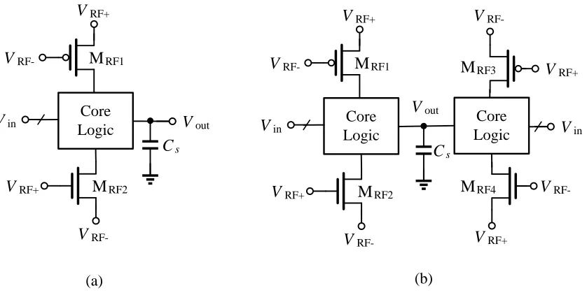
The RF-only logic is a dual-rail, AC-powered logic. There are two types of RF-only logic as shown in Figure 2.1: single phase which utilizes only half of the RF cycle and dual phase which utilizes the full RF cycle [5]. In this chapter, we focus on the analysis of the single-phase RF-only logic.
RF+ V RF-V RF+ V RF-V RF1 M out V Core Logic RF2 M in V s C Core
Logic Vin
RF-V RF-V RF+ V RF+ V RF3 M RF4 M RF+ V RF-V RF+ V RF-V RF1 M out V Core Logic RF2 M in V s C (a) (b)
Figure 2.1 Generic structure of the RF-only logic gate. It consists of a logic evaluation part (Core Logic) and a set of power supply transistors (a) single phase (b) dual phase
2.2
Circuit Operations
The single-phase RF-only inverter shown in Figure 2.2(a) is used to illustrate the operations of RF-only logic, with the applied RF signals shown in Figure 2.2(b). There are two operating phases based on the operating regions of the power supply transistors. The evaluation phase: when VRF+− VRF- >VL, where VL is given by Equation (2.1) [13]. VL is the minimum voltage for a metal-oxide-semiconductor (MOS) channel to be in weak inversion:
VL = VFB+ ϕ
where VFB is the transistor flat-band voltage, ϕF is the Fermi potential, Vsb is the source to body voltage, and γ is the body effect coefficient.
RF+
V
RF-V MRF1
RF2 M RF+ V RF-V in
V Vout
s C 1 M 2 M Storage Phase Ton RF
RF+ cos( t )
V =A ω φ+
RF
RF- cos( t )
V =−A ω φ+
L
V
0
t= t =Ton
(a) (b)
Figure 2.2 (a) Schematic of an RF-only inverter (b) Differential supply signals with operating regions indicated
Ton =
arccos VL 2ARF πfRF
(2.2)
where fRF and ARF are the frequency and amplitude of the RF signal, respectively. The RF supply signals VRF+ and VRF- are defined as
VRF+ = ARFcos(ωt+ϕ) (2.3)
VRF- = -ARFcos(ωt+ϕ) (2.4)
where
VRF+(0) = VRF+(Ton) = VL
2 (2.5)
Operations of the RF-only inverter in both steady-state and logic transitions are analyzed in the following section using first order RC model.
2.2.1 Steady-State Analysis
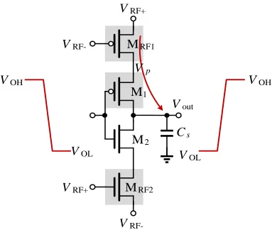
RF+ V
RF-V MRF1
RF2 M RF+ V RF-V out V s C 1 M 2 M p V in low V = RF+ V
RF-V MRF1
RF2 M RF+ V RF-V out V s C 1 M 2 M p V in low V = (a) (b) RF+ V RF-V RF1 M out V s C 1 R p V gd C RF+
V Vout
s C 1 R RF1 R p V
Figure 2.3 (a) Equivalent circuit of the RF-only inverter in the evaluation phase when Vin = VOL (b) Equivalent circuit of the RF-only inverter in the storage phase when Vin = VOL
Figure 2.4 Simulated waveforms of the RF-only inverter in the steady-state when Vin = VOL. VOH
is defined as the output voltage during the storage phase
During the storage phase, the two power supply transistors M and M are turned -0.5 0 0.5 Voltage (V ) VRF+ V
RF-0 0.3 0.6 0.9 1.2 1.5
equivalent circuit of the inverter in the storage phase is shown in Figure 2.3(b). The negative RF signal VRF- is fed through to the output node via capacitive coupling effect of Cgd. Its impact on the output voltage is trivial since Cs is orders of magnitude larger than Cgd. To simplify the analysis, we assume the output voltage stays constant during the storage phase. The simulated output voltage in the storage phase verifies this assumption as shown in Figure 2.4. We further define the high and low output levels VOH, VOL as the corresponding output voltages during the storage phase. We assume the transistors are sized to achieve a balanced driving strength for pull up and pull down networks so that VOH = −VOL.
During the evaluation phase, MRF1 and M1 are turned on and can be modeled as average “on” resistors RRF1 and R1. The equivalent circuit is shown in Figure 2.3(a). It is equivalent to a track-and-hold circuit. The output voltage Vout tracks the RF supply signal VRF+ with a phase delay defined by the time constant τ = (R1+ RRF1)Cs. Applying phasor analysis on the equivalent circuit and considering the initial condition of Vout(0) = VOH, the output voltage Vout as a function of time can be derived as
Vout = (VOH- ARF
√1+ω2τ2cos(ϕ+ θ))e - tτ
+ ARF
√1+ω2τ2cos(ωt+ ϕ+ θ) (2.6)
defined by the initial condition, and a magnitude-attenuated and phase-shifted version of the RF signal VRF+. At the end of the evaluation phase, Vout settles to VOH, yielding
VOH = ARF
√1+ω2τ2(1-e- Tτon)
(cos(ωTon+ ϕ+ θ) - e- Tτoncos(ϕ+ θ)) (2.7)
Equation (2.7) unveils the DC output voltage level that can be achieved with the single-phase RF-only logic circuits. To capture more trackable expressions of Vout and VOH, let’s consider two typical operating scenarios defined by the RF cycle time and the time constant τ. Note that the RF-only logic operates in the large signal domain in which the transistors
exhibit considerable non-linearity; therefore, the first order analysis conducted in this section is intended to gain design insights rather than to derive accurate models.
• TRF≫τ (high RF amplitude and low RF frequency), the decaying initial transient
response can be ignored and the phase shift θ≈ -arctan (0) = 0. It leads to the simplified output voltage Vout and VOH as
Vout = ARFcos(ωt+ ϕ) (2.8)
VOH = ARFcos(ωTon+ ϕ) = VRF+(Ton) = V𝐿𝐿
2 (2.9)
voltage V𝐿𝐿. The output node exhibits large voltage ripples during the evaluation phase, which leads to excessive static power consumption and reduced noise margin. • TRF≪τ (low RF amplitude and high RF frequency), the phase shift θapproaches π/2.
Under these conditions, we have
e- τt≈ 1- t/τ (2.10)
�1+ω2τ2 ≈ ωτ (2.11)
The output voltage Vout and VOH can be simplified as
Vout = (VOH- ARF
ωτ sin(ϕ))(1 - t τ) +
ARF
ωτ sin(ωt+ ϕ) (2.12)
VOH = 2ARF ωTon
sin(ωTon+ ϕ) = ARF arccos V𝐿𝐿
2ARF
sin(ωTon+ ϕ)= ARFsin(α)
α (2.13)
where α is the evaluation angle defined as α = ωTon+ ϕ = arccos VL
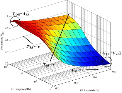
2ARF. The steady-state logic level VOH is almost equal to ARF; therefore, the voltage ripple during evaluation phase is minimized.
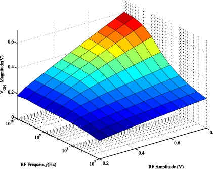
VOH normalized to the RF amplitude ARF. For a constant RF frequency, VOH is linearly proportional to RF amplitude ARF. As RF frequency increases, this proportional coefficient increases as well. For a constant RF amplitude, the VOH gets closer to ARF as RF frequency increases.
0.2
0.4
0.6
0.8
107 108
109 1010
0.2 0.4 0.6 0.8 1
RF Amplitude (V) RF Frequency(Hz)
N
o
rm
al
ized
V OH
=
RF
τ
T
RF
τ
T
<<RF
τ
T
>> RFOH
V
≈A
OH L
V
≈V /2
Figure 2.6 The output logic high VOH as a function of RF amplitude and frequency, normalized to
2.2.2 Dynamic Operation Analysis
Dynamic operation analysis addresses the operation characteristics in the present of logic transitions. The following discussion proceeds under the assumption that the input signal to the inverter abruptly changes from VOH to VOL at the beginning of the evaluation phase. The dynamic operation of an RF-only inverter features different behavior in the two operating scenarios as we defined in the steady-state analysis.
• TRF ≫τ: a logic transition can complete within one RF cycle, and the output
capacitance C𝑠𝑠 is charged up directly by the supply current through the equivalent resistors RRF1 and R1. A simulated waveform of an inverter working under this scenario is shown in Figure 2.7 to illustrate the logic transition. The output voltage Vout can be derived in the same approach as we did in the steady-state analysis, only with a different initial condition Vout(0) = VOL,
Vout = (VOL- ARF
√1+ω2τ2cos(ϕ+ θ))e - τt
+ ARF
Figure 2.7 Simulated transient response of a logic transition for an RF-only inverter operating at TRF ≫τ
• TRF ≪τ: a logic transition takes multiple consecutive RF cycles to finish as shown in
Figure 2.8. In the evaluation phases, the output capacitance C𝑠𝑠 is charged directly by the supply current through the equivalent resistors RRF1 and R1. In the storage phases, the charges on Cs are retained. For each evaluation phase during the logic transition, the output voltage can be derived as
Vout(i) = (Vi-1- ARF
√1+ω2τ2cos(ϕ+ θ))e - tτ
+ ARF
√1+ω2τ2cos(ωt+ ϕ+ θ) (2.15)
Figure 2.8 Simulated transient response of a logic transition for an RF-only inverter at TRF ≪τ
For the following analysis of propagation delay and power consumption, we derive tractable equations for parameters of interest based on the equivalent RC circuits.
Simulations help to determine these characteristics in the transition region between these two scenarios we discussed.
2.3
Propagation Delay
assume that the input transition happens exactly at the beginning of the evaluation phase and the load capacitance Cs is constant during the logic transition. The leakage current and capacitive coupling effect on load capacitance Cs are also ignored. Figure 2.9 shows the equivalent circuit of an RF-only inverter during a high-to-low logic transition. Transistors MRF1 and M1 are modeled as average “on” resistors in series, through which the load capacitance Cs is charged up. The load capacitance analysis of RF-only logic is identical to the classic CMOS circuit [14].
RF+ V RF-V RF+ V RF-V s C RF1 M 1 M out V RF2 M 2 M p V OL V OH V RF+
V Vout
s C
1
R
RF1
R Vp
Figure 2.9 Equivalent circuit of a single-phase RF-only inverter during a high-to-low logic transition
2.3.1 TRF >> τ: Single-RF-Cycle Transition
Vout = (VOL- ARF
√1+ω2τ2cos(ϕ+ θ))e - τt
+ ARF
√1+ω2τ2cos(ωt+ ϕ+ θ) (2.16)
Given the propagation delay Tp is defined as
Vout�Tp� = 0 (2.17)
Substitute Equation (2.17) into Equation (2.16), and solve for Tp, we can obtain
Tp = τ lnVOH+V0
Vp ≈ τln2 (2.18)
where
VOH = ARFcos(ωTon+ ϕ) (2.19)
V0 = ARF
√1+ω2τ2cos(ϕ+ θ) (2.20)
Vp = ARF
√1+ω2τ2 cos(ωTp+ ϕ+ θ) (2.21)
2.3.2 TRF ≪τ: Multiple-RF-Cycle Transition
During a multiple-RF-cycle logic transition, the output capacitance is charged in evaluation phase and retains the charges in the storage phase. A logic transition finishes within multiple consecutive evaluation phases. Assuming the output voltage takes n RF cycles to reach half of the peak-to-peak value, the overall propagation delay can be expressed as
Tp = (n-1)TRF+Tn (2.22)
where Tn is the transition time of the last RF cycle. We derive the output voltage in the last RF cycle in the same way as Equation (2.16), yielding
Vout(n) = (Vn-1- ARF
√1+ω2τ2cos(ϕ+ θ))e - tτ
+ ARF
√1+ω2τ2cos(ωt+ ϕ+ θ) (2.23)
with Vout(n) the output voltage in the n-th RF cycle, Vn-1 the initial output voltage in the n-th RF cycle, respectively. To solve for Tp, the cycle count n and transition time Tn must be solved first. To simplify the solution, we assume that Tn = Ton. According to the propagation delay definition, we have
Vout(n)(Ton) = 0 (2.24)
Vi = (Vi-1 - ARF
√1+ω2τ2cos(ϕ+ θ))e - Tτon
+ ARF
√1+ω2τ2cos(ωTon+ ϕ+ θ) (2.25)
Also, in the first RF cycle, we have
V1 = (VOL- ARF
√1+ω2τ2cos(ϕ+ θ))e - Tonτ
+ ARF
√1+ω2τ2cos(ωTon+ ϕ+ θ) (2.26)
There are n unknowns, being V1…Vi…Vn, and n equations as in the same pattern of Equation (2.25) for each unknown. Solving these n equations for Vn, and substituting Equation (2.26) into the results, we can derive
Vn = V1 + (V1+ VOH) e
- Tonτ
1-e-
Ton
τ
(1- (e-
Ton
τ )
n-1
)= 0 (2.27)
Given that TRF ≪ (RRF1+R1)Cs holds for the multiple-RF-cycle transition scenario, Equation (2.26) hence can be simplified and re-arranged as
V1 = VOL(1 - 2Ton
τ ) (2.28)
n = [log
(τ-Tτon)0.5 ] + 1 (2.29)
We define the effective evaluation time as
Teff = Ton τ =
arccos V𝐿𝐿 2ARF πfRFτ
(2.30)
Finally substitute Equation (2.30) into Equation (2.29), we can obtain the expression for multiple-RF-cycle propagation delay
Tp = - 0.7
ln(1-Teff)TRF + Ton (2.31)
Since the effective evaluation time Teff is linearly proportional to the RF amplitude ARF from Equation (2.30), the propagation delay Tp is reversely proportional to ln(1-ARF) from
Equation (2.31).
2.3.3 Simulation Results
we will discuss in next section. The same ring oscillator consists of classic CMOS inverters was also simulated for comparison. The default simulation settings are listed in Table 2.1.
Table 2.1 Default parameters for propagation delay simulations
Inverter Size 400nm/160nm
PST size 400nm/160nm
RF amplitude 500mV
RF frequency 1GHz
Data rate 1Mbps
Load 10fF
Transition time 1ps
Figure 2.10 shows the simulated oscillation periods in logarithmic scale as a function of the RF amplitude for both designs. The supply voltages were set to the same root-mean-square (rms) values for fair comparison. Two observations can be drawn from the results:
• The propagation delay of RF-only logic versus supply level features the same trend as
the classic CMOS as we discussed in the first-order analysis. The delay is relatively insensitive to supply variations for high power level. However, it decreases in logarithmic relation with the power supply when the power level decreases below 0.4V as the transistors operate in the sub-threshold region.
• For the same rms voltage level, the RF-only logic based ring oscillator runs slower in
penalty due to storage phase. For the same rms voltage level, the peak-to-peak overdrive voltage across RF-only transistors is higher than classic CMOS gate transistors which are powered by a DC supply. In the super-threshold region where the delay is insensitive to power supply variation, the delay penalty due to storage phase dominates. Therefore, RF-only logic based ring oscillator runs slower. Whereas in the sub-threshold region, the propagation delay has an exponential relation with the power level, thus the RF-only logic based ring oscillator powered by a higher
overdrive voltage runs faster.
Figure 2.10 Oscillation periods of ring oscillator based on RF-only logic and classic CMOS logic as a function of RF amplitude
0.2 0.3 0.4 0.5 0.6 0.7 0.8 0.9 1 1.1 1.2
101
102
103
O
sc
illa
tio
n
P
er
io
d
(
n
s)
Supply Voltage (Vrms)
The impact of RF frequency on propagation delay is explored by simulating the ring oscillator under different RF frequencies. The results are plotted in Figure 2.11. Overall, the gate delay is insensitive to RF frequency and slightly decreases as the frequency increases. However, some non-monotonic data points observed due to the delay penalty caused by the phase relation of RF signal and input transition. As RF frequency increases, additional storage phases may be added to the transitions which lead to a longer delay.
In summary, the propagation delay of RF-only logic is a strong function of the RF amplitude and weakly impacted by the RF frequency.
Figure 2.11 Oscillation periods of RF-only logic based ring oscillator as a function of RF frequency
10-1 100
38 39 40 41 42 43 44 45 46
O
sc
illa
tio
n
P
er
io
d
(
n
s)
RF Frequency (GHz)
2.3.4 Other Parameters
We assumed the input logic transition happened exactly at the beginning of the evaluation phase to simplify the analysis. However, the logic transitions can occur at any time during the evaluation phase. The propagation delay is not constant and varies with the phase relationship between the input transition and the RF supply. Simulation of propagation delay of an RF-only inverter versus transition phase shows a delay penalty for the transitions happening close the end of evaluation phase. The simulation results are plotted in Figure 2.12 with the delay penalty annotated. Note the penalty usually equals the length of storage phase. This effect is reduced for logic path consisting of multiple gates. However, enough timing margin needs to be added to compensate for the delay penalty in logic design and synthesis.
0 0.4 0.8 1.2 1.6
0 0.2 0.4 0.6 0.8 1
P
ropa
ga
ti
on D
el
ay (
ns
)
Logic Transition Phase (degree)
Delay Penalty
The propagation delay of the RF-only inverter is simulated as a function of the core logic sizing and the results are plotted in Figure 2.13. It indicates an optimal W/L ratio which minimizes the propagation delay. Further increasing the W/L ratio beyond the optimal point leads to the intrinsic capacitance dominating output capacitance and a longer delay.
Figure 2.13 Simulated propagation delay of the RF-only inverter as a function of the core logic sizing
The propagation delay of the RF-only inverter is simulated as a function of power supply transistor sizing, and the results are plotted in Figure 2.14. Increasing PST width reduces the propagation delay with a diminishing return, due to the effective “on” resistance R1
Figure 2.14 Simulated propagation delay of RF-only inverter as a function of power supply transistor sizing
2.4
Power Consumption
The power consumption of a CMOS circuit consists of dynamic and static consumption [14]. Dynamic power consumption results from the charging and discharging of capacitances while input switches and static power consumption is defined as the power dissipated in the absence of switching activity. The power consumption of RF-only logic circuits consists of the following four parts:
• Dynamic power dissipation of charging output capacitance • Dynamic power dissipation of direct-path current
• Static power consumption of capacitive coupling
Compared to conventional CMOS circuit, the RF-only logic circuits dissipate more static power due to the RF feedthrough to the output nodes during the evaluation phase. While the dynamic power consumption is not a function of (TRF /τ), static power consumption reduces as (TRF /τ) decreases. This is analyzed in detail in the following section.
2.4.1 Dynamic Power: Charging Output Capacitance
Schematic of a single phase RF-only logic inverter is shown in Figure 2.15. Upon a high-to-low input switch, the output capacitance Cs gets charged to VOH or VOL. The energy drawn from the power supply is dissipated on the transistors along the charging path; whereas the energy stored on Cs keeps constant. The following analysis of dynamic power consumption is conducted in the two scenarios same as the propagation delay analysis.
RF+ V RF-V RF+ V RF-V s C RF1 M 1 M out V RF2 M 2 M p V OL V OH V OL V OH V
a. TRF>>τ
A precise measurement for the energy consumption can be derived. Let’s first consider the low-to-high logic transition. We assume, initially, that the input waveform has zero rising and falling time. The energy taken from the supply VRF+ during one transition can be derived by integrating the instantaneous power over the period of interest:
ERF = � VRF+iRF(t)
∞
0
dt = � ARFcos(ωt+ ϕ)CsdVout dt
∞
0
dt = � ARFcos(ωt+ ϕ)CsdVout
VOH
VOL
(2.32)
To derive a tractable equation for the dissipated energy, we first calculate half of the energy drawn. It is the energy dissipated up to Vout reaching half output swing:
ERF
2 = � VRF+iRF(t)
Tp
0
dt = � ARFcos(ωt+ ϕ)Cs dVout
0
VOL
(2.33)
As mentioned in the delay analysis, the output voltage of single-RF-cycle transition in Equation (2.16) can be simplified under the condition of TRF ≫τ as
Vout = ( VOL - ARFcos(ϕ) )e-
t
τ + ARFcos(ωt+ ϕ) (2.34)
VRF+(0)= ARFcos(ϕ)=V𝐿𝐿
2 (2.35)
Vout(Tp) = 0 (2.36)
VOH = V𝐿𝐿
2 (2.37)
Substitute Equations (2.34)(2.35)(2.36)(2.37) into Equation (2.33), and solve for energy dissipation
ERF = CsVOH2 (5 - 12e-
2Tp
τ ) (2.38)
Substituting the expression of propagation delay Tp from Equation (2.18) into Equation (2.38), we can derive a more straightforward equation for energy consumption similar to the conventional CMOS circuits as
ERF≈ 2CsVOH2 (2.39)
We can also confirm that the energy drawn from the RF source and stored on output capacitor Cs at the end of transition is zero:
ECs = � VoutiRF(t)
∞
0
dt = � VoutCsdVout dt
∞
0
dt = Cs� VoutdVout
VOH
VOL
Notice that not like conventional CMOS circuits, no extra energy is stored on the output capacitance. All the energy drawn from the RF source is dissipated on the transistors along the charging path. These results can also be derived for a high-to-low logic transition. In summary, each logic transition takes a fixed amount of energy, equal to 2CsVOH2 . Therefore, for one on-and-off transition, the dynamic energy dissipated is
ERF = 4CsVOH2 = Cs(2VOH)2 (2.41)
The dynamic energy consumed is equivalent to the dynamic energy dissipation of a
conventional CMOS inverter with a power supply of 2VOH. If the gate is switched on and off fs times per second, the dynamic power consumption is given by
Pdyn = 4CsVOH2 fs = Cs(2VOH)2fs (2.42)
b. TRF≪τ
During a multiple-RF-cycle logic transition, the dynamic energy dissipated can be defined as
ERF =� � VRF+Cs
Vi+1
Vi
dVout
m
i=1
where m is the number of RF cycles for the logic transition to finish, and Vi is the output voltage at the end of the i-th RF cycle. The energy dissipated during the (i+1)-th cycle is
Ei+1 =� VRF+Cs
Vi+1
Vi
dVout(i+1) (2.44)
where the (i+1)-th output voltage can be rewritten under the condition of TRF ≪τ as
Vout(i+1) = (Vi - ARF
ωτ sin(ϕ)) (1 - t τ) +
ARF
ωτ sin(ωt+ ϕ) (2.45)
Substitute Equation (2.25) and (2.45) into Equation (2.44) and we can obtain the energy consumed during the (i+1)-th RF cycle as
Ei+1 = CsTon 4τ �2ARF
2
+ VLVOH�- Ton
2
Cs 2τ2 VOH
2
- CsTon
τ ViVOH (2.46)
Substitute Equation (2.46) back to Equation (2.43) and we can get
ERF = m�CsTon 4τ �2ARF
2 + V
LVOH� -
Ton2 Cs 2τ2 VOH
2 �- CsTon
τ VOH�Vi m
i=1
To solve ERF, we need to substitute Vi with known values. Recall that for the (i+1)-th RF cycle, the output voltage is already derived and is repeated here
Vi+1 = (Vi - ARF
ωτ sin(ϕ)) (1 - Ton
τ ) + ARF
ωτ sin(ωTon+ ϕ) (2.48)
Substitute Equation (2.25) into Equation (2.48) and re-arrange it, we can obtain
Ton
τ Vi = Vi - Vi+1 +
Ton
τ (VOH -
Ton
2τ ) (2.49)
Substitute Equation (2.49) into Equation (2.47) and re-arrange it, we can derive the dynamic energy dissipated during one multi-RF-cycle transition as
ERF = 2CsVOH2 + m (CsTon 4τ �2ARF
2
+ VLVOH - 4VOH2 � ) (2.50)
We show later in the next section that m (CsTon
4τ �2ARF 2
+ VLVOH - 4VOH2 � ) is the static energy dissipated due to RF feedthrough in the evaluation phase. Therefore, the dynamic energy consumption due to logic transition is
This result is identical to the one we derived in the single-RF-cycle transition case. No extra energy is stored on the output capacitance, and all the energy drawn from RF source is dissipated during the logic transition. These results can also be derived during the high-to-low transitions. In summary, each logic transition takes a fixed amount of energy, equal to 2CsVOH2 . If the gate is switched on and off fs times per second, the power consumption is given by
Pdyn = 4CsVOH2 fs = Cs(2VOH)2fs (2.52)
Figure 2.16 Dynamic power consumption of RF-only inverter and classic CMOS inverter as a function of supply level
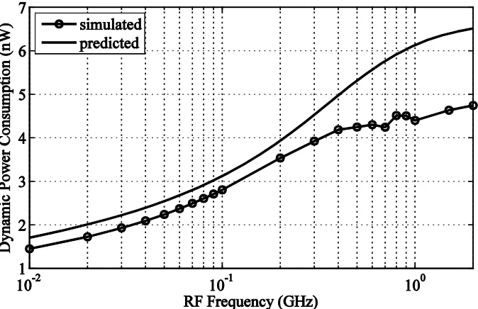
Figure 2.17 shows RF frequency’s impact on dynamic power consumption. VOH
increases as RF frequency increases, resulting in more dynamic power dissipated. At high RF frequency, the circuit operates in TRF ≪τ region and VOH close to ARF, resulting in a
flattened dynamic power consumption.
0.2 0.3 0.4 0.5 0.6 0.7 0.8 0.9 1 1.1 1.2
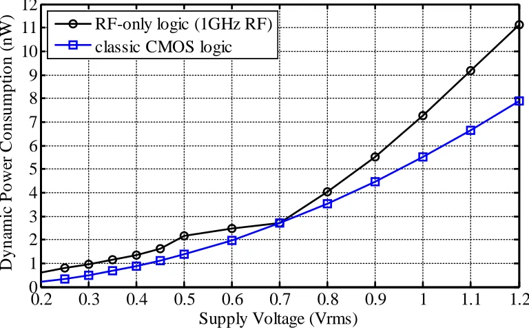
0 1 2 3 4 5 6 7 8 9 10 11 12 D yna m ic P ow er C ons um pt ion ( nW )
Supply Voltage (Vrms) RF-only logic (1GHz RF)
Figure 2.17 Dynamic power consumption of an RF-only inverter as a function of RF frequency fRF, both simulated and predicted included.
2.4.2 Dynamic Power: Direct-Path Current
RF+ V
RF-V
RF+ V
RF-V
s
C RF1 M
1 M
out
V
RF2 M
2 M
p
V
OL
V
OH V
OL
V
In reality, the input signal changes gradually, which results in a direct current path between the two power supplies for a short period during the logic transition. We follow the same derivation as shown in [14], the average power consumption due to direct-path current is
Pdp = 2tscARFIpeakfs (2.53)
where
tsc = 2ARF- 2VL 2ARF
2Tp
0.8 = 2.5Tp
ARF- VL
2ARF (2.54)
Ipeak is determined by the saturation current of the devices and is hence directly proportional to the size of the transistors [14].
2.4.3 Static Power: RF Feedthrough
Not like the conventional CMOS circuits, the RF-only logic circuits dissipate a
RF+ V RF-V RF+ V RF-V s C RF1 M 1 M out V RF2 M 2 M p V OL
V Vout
s C 1 R RF1 R RF+ V
Figure 2.19 Equivalent circuit of the RF-only inverter in evaluation phase with the charging and discharging path labeled
Consider the case of an inverter with input set to logic low, and the equivalent circuit is pictured in Figure 2.19. The energy taken from the supply VRF+ during one RF cycle can be derived by integrating the instantaneous power over the evaluation period:
ETH = � VRF+iRF(t)
Ton
0
dt = � ARFcos(ωt+ ϕ)CsdVout dt
Ton
0
dt (2.55)
In the scenario of TRF>>τ, the overall energy dissipated ETH approaches zero since there is approximately no phase shift between the RF source and output voltage.
Vout = (VOH - ARF
ωτ sin(ϕ))(1 - t τ) +
ARF
ωτ sin(ωt+ ϕ) (2.56)
VOH = 2ARF ωTon
sin(ωTon+ ϕ) = ARFsin(α)
α (2.57)
Substitute Equations (2.56) and (2.57) into Equation (2.55), the energy dissipated during steady-state evaluation phase can be expressed as
ETH = CsTon 4τ �2ARF
2
+ VLVOH - 4VOH2 � = Ton 4τ ARF
2
Cs (1 + sinαcosα
α
-2sinα2
α2 ) (2.58)
The power dissipated can be obtained by multiplying ETH with RF frequency fRF
Pth = TonfRF 4τ ARF
2
Cs (1 + sinαcosα
α -
2sinα2
α2 ) (2.59)
Substitutes Ton in Equations (2.2) into Equation (2.59) and yield the following expression for Pth
Pth = K
4(R1 + RRF1)ARF
2
(2.60)
K = α π(1+
sinαcosα
α -
2sinα2
α2 ) (2.61)
Note that Equation (2.60)(2.61) only valid under the condition of TRF ≪τ, where α is close to zero. Since effective on-resistance (R1 + RRF1) is inversely proportional to the RF amplitude, the static power consumption under this condition has a cubical relationship with RF
amplitude as shown in Equation (2.60).
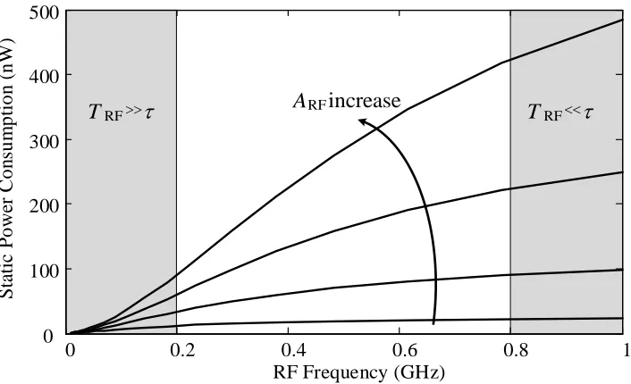
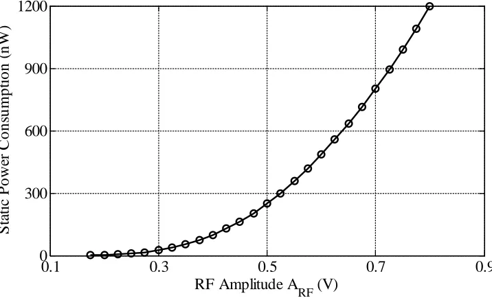
As RF frequency increases, the operating region moves from TRF>>τ to TRF ≪τ, thus the power dissipation increases. This relationship is also captured in the simulation and plotted in Figure 2.21. Power dissipation increases approximately linearly with RF frequency in the transition region. In TRF ≪τ region, power consumption is simulated as a function of amplitude and plotted in Figure 2.22. As predicted from our first order analysis, the static power increases cubically with RF amplitude in this region.
0 0.2 0.4 0.6 0.8 1
0 100 200 300 400 500 S ta tic P o w er C o n su m p tio n ( nW )
RF Frequency (GHz)
RF
T >>τ ARFincrease TRF<<τ
Figure 2.22 Simulated static power consumption of RF-only logic as a function of RF amplitude in TRF ≪τ region
2.4.4 Static Power: Capacitive Coupling
The capacitive coupling effect, which causes RF supply signal feeding through to output node, exists during the entire RF cycle. However, due to its limited effect on the output node, it only dominates during the storage phase while power transistor MRF1 is off. Considering the case of an inverter with input set to logic low, the energy taken from the supply V RF-during one RF cycle can be derived by integrating the instantaneous power over one RF period:
ECC = � VRF+iRF(t)
TRF
0
dt = � ARFcos(ωt+ ϕ)CsdVout dt
TRF
0
dt (2.62)
0.1 0.3 0.5 0.7 0.9
0 300 600 900 1200 S ta ti c P ow er C ons um pt ion ( nW )
In the scenario of TRF>>τ, the overall energy dissipated ECC = 0 since there is no phase shift between RF source and output voltage. In the scenario of TRF ≪τ, the capacitive coupling power can be derived as
Pcc = τ 2ARF
2
Cs (2.63)
Power consumption due to capacitive coupling is orders of magnitude lower than other power dissipation sources, and we can usually ignore its contribution.
2.4.5 Put It All Together
The total power consumption of the RF-only inverter is now expressed as the sum of its four components:
Ptot= Pdyn+ Pdp+ Pth+ Pcc (2.64)
Table 2.2 Summary of power consumption of RF-only logic
TRF ≫𝝉𝝉 TRF ≪𝝉𝝉 ARF fRF W/L fs
Pdyn Cs(2VOH)2fs O(n) - Optimal O(n)
Pdp 2tscARFIpeakfs O(n2) - - O(n)
Pth 0 K
4(R1 + RRF1)ARF
2
O(n3) O(n) O(n) -
Pcc 0 τ
2ARF
2
Cs O(n3) - Optimal -
The capacitive dynamic power dissipation and static consumption are the dominant factors. A family of contour curves that represent the operating points at which power dissipation due to these two components are equal are shown in Figure 2.23. For each curve, the area beneath is the dynamic-power-dominant area. For low power designs, it is better to set the operating point of the circuit in the dynamic power dominant region. Note that they are not constant power consumption contours. The curves extend up to ARF = 500mV to ensure fRF/fs > 10 for robust operation, and the lower boundary stops at 100mV to prevent too large propagation delay to sustain the data rate.
Figure 2.23 Contours of operating points at which the capacitive dynamic power dissipation equals static power consumption
2.5
Robustness
In this section, the robustness of RF-only circuit is investigated mainly through the analysis of an RF-only inverter’s noise margin, and how the noise margin is impacted by the RF amplitude and frequency. Following that, the operating ranges of RF amplitude and frequency are identified based on the worst case Static Noise Margin (SNM) analysis.
0.1 0.2 0.3 0.4 0.5 0.6
100
101
102
103
R
F
F
req
u
en
cy
(
M
H
z)
RF Amplitude ARF (V)
f
s=100KHz
fs=300KHz
f
s=1MHz
f
2.5.1 Noise Margin Analysis
Due to the output voltage ripples in steady-state, the noise margin of RF-only logic is smaller compared to the conventional CMOS logic with the same power supply amplitude (VDD=2ARF). Furthermore, it is not intuitive to derive an analytical expression for RF-only logic’s noise margin based on the well-known “mirror-and-maximum square method” [15], since the voltage transfer function is not monotonic due to the voltage ripples. Instead, we leverage the worst case SNM which is easily determined by circuit simulation to evaluate circuit robustness and study how it varies with design parameters [15]. The simulation methodology based on cross-coupled inverters with a series noise source that emulates an infinite inverter chain is adopted here [16].
Figure 2.24 Simulated worst case SNM of an RF-only inverter as a function of RF frequency (ARF
= 0.5V)
The simulated worst-case SNM and the SNM normalized to the RF amplitude of an RF-only inverter are plotted in Figure 2.25. It is observed that as RF amplitude decreases, the SNM deteriorates due to reduced output swing. Moreover, inspecting the normalized SNM provides the following insights:
• In the super-threshold region, as ARF decreases, the normalized SNM increases. Two
• In the sub-threshold region, the normalized SNM decreases as ARF decreases. This is
a result of deterioration of the gate characteristic while the transition region gain approaches one.
0.1 0.2 0.3 0.4 0.5 0.6 0.7
0 0.1 0.2 0.3 0.4 S ta tic N o is e M ar g in ( V )
RF Amplitude (V)
0.1 0.2 0.3 0.4 0.5 0.6 0.70.4 0.6 0.8 1 1.2 N o rm a liz ed S ta tic N o is e M ar g in SNM Normalized SNM